國 立 交 通 大 學
電信工程學系
碩 士 論 文
一個操作在 1.25 Gb/s 具備降低抖動能力突發式時脈
資料回復電路
A 1.25 Gb/s Burst-Mode Clock and Data Recovery
Circuit Using the Jitter Reduction Technique
研究生:游凱迪
指導教授:闕河鳴 博士
一個操作在 1.25Gb/s 具備降低抖動能力突發式時脈資料回
復電路
A 1.25Gb/s Burst-Mode Clock and Data Recovery Circuit
Using the Jitter Reduction Technique
研 究 生:游凱迪 Student: Kae-Dyi You
指導教授:闕河鳴 博士 Advisor: Dr. Herming Chiueh
國 立 交 通 大 學
電 信 工 程 學 系 碩 士 班
碩 士 論 文
A Thesis
Submitted to Department of Communication Engineering College of Electrical and Computer Engineering
National Chiao Tung University in Partial Fulfillment of the Requirements
for the Degree of Master of Science
in
Communication Engineering
January 2009
Hsinchu, Taiwan, Republic of China
一個操作在 1.25 GB/s 具備降低抖動能力突發式時脈資料回
復電路
研究生:游凱迪 指導教授:闕河鳴 博士 國立交通大學 電信工程學系碩士班摘要
一具備降低抖動功能的突發式時脈及資料回復電路被實現在本研究,並將其 應用於被動光纖網路系統。此電路使用了半速率架構並操作在 1.25-Gb/s。在此 時脈及資料回復電路中,我們在邊緣偵測器裡使用了一個半位元時間延遲產生電 路來改善抖動的累積:此乃藉由一個具備多組延遲時間值的延遲時間產生電路來 產生;並利用動態平均的概念來產生半位元的時間延遲以造成最小的抖動產生。 本晶片使用 0.18 μm 互補式金氧半製程來製造,量測到的回復時脈訊號在抖動降 低技術未啟動時的峰對峰抖動值為 130ps;在抖動降低技術啟動後的峰對峰抖動 值為 114.3ps,改善了 13.7%。當操作電壓為 1.8V 之下,整個時脈與資料回復電 路的功率消耗為 36mW。晶片面積為 0.99 × 0.97mm2 。Abstract
A 1.25 GB/s Burst-Mode Clock and Data Recovery Circuit
Using the Jitter Reduction Technique
Student: Kae-Dyi You Advisor: Dr. Herming Chiueh
SoC Design Lab, Department of Communication Engineering,
College of Electrical and Computer Engineering, National Chiao Tung University Hsinchu 30010, Taiwan
Abstract
A 1.25-Gb/s half rate Burst-Mode clock and data recovery (BMCDR) circuit with jitter reduction technique for PON application is presented in this thesis. There are several delays in the half of bit time (Tbit/2) delay generating circuit of the edge
detector to create a delay time that falls exactly on half of bit time (Tbit/2) delay to
minimize jitter generation. The measured peak to peak recovered clock jitter when the jitter reduction technique is disable is 130ps; while the jitter reduction technique is active, the measured peak to peak clock jitter is 114.3ps, reduced by 13.7%. The chip was fabricated with TSMC 0.18 μm CMOS technology. The die area of the CDR is 0.99 × 0.97 mm2, and power consumption is 36mW under a 1.8-V supply voltage.
Acknowledgment
本篇碩士論文得以順利完成,首先要感謝的是我的指導教授---闕河鳴博 士。在實驗室的日子裡,闕老師不管在研究方面或生活處事上的指導,都讓我獲 益良多。老師特別注重學生獨立思考和口語表達以及整理文件的能力,給予剛接 觸電路設計研究的我正確的研究態度及方法;當研究遇到瓶頸時,老師也總能適 時鼓勵我以積極的態度面對問題。同時也感謝張振豪教授、郭建男教授、林俐如 博士等口試委員們撥空來參加口試,並給予我寶貴的意見使我的論文內容能夠更 完整。 接著我想要感謝我的父母及妹妹,謝謝你們的支持以及體諒,讓我在研究所 的求學過程中沒有經濟上的後顧之憂,能夠專心的為夢想打拼,雖然你們可能一 輩子也會不知道我在做什麼研究,但沒有你們的栽培,我不會有今天這些研究成 果,我以你們為榮。另外,感謝女友凱勵,對我無怨無悔的付出及關心。 其次,謝謝在 526 實驗室或已畢業的學長們,感謝嘉儀、佐昇、順華、江俊、 信太及俊誼等諸多學長在研究上或是日常生活上對我的照顧;還要謝謝秉勳、品 翰、明君、春慧四位同窗好友平日在我的課業及生活上的幫忙;也謝謝是瑜、鎮 宇、國哲、鼎國、燦杰、登政等學弟們的支持與協助;其中非常感謝燦杰在最後 量測時給予我在 matlab 上面的技術支援;還有其他研究群很多關心我畢業狀況 的順維、國忠、國權、188、seechi、世豪、資閔、威文、晟佑、宗恩、暄泰平 常在研究領域上的討論及切磋,讓我的基本觀念能夠更加的紮實。最後還要特別 謝謝大學同學董大、約廷等人對我在類比電路設計領域的幫助。另外要感謝 626 實驗室的子超及中興大學的信民,謝謝有你們在量測上的幫忙,沒有你們,我的Acknowledgment 兩年半的日子裡有這麼快樂且充實的研究生活,謝謝大家讓我能順利的完成學 業。 我謹將這篇論文獻給上述曾提攜或幫助過我的你們,謝謝大家並祝福大家。 游凱迪 于 風城交大 98 年 冬
Content
中文摘要
………..…….. I
English Abstract……….. II
Acknowledgement……….
III
Content………....
V
List of Tables………..
VII
List of Figures………VIII
Chapter 1
Introduction
1
1.1 Introduction of Clock and Data Recovery Circuit ... 1
1.2 Specification of GPON ... 1
1.3 Motivation ... 2
1.4 Organization ... 3
Chapter 2 Introduction of the GVCO-Based Burst-Mode Clock and
Data
Recovery
Circuit
4
2.1 Literature Review... 4
2.2 Design Challenges of Burst-Mode CDR... 6
2.3 Jitter Issue in Conventional Burst-Mode CDR ... 7
Chapter 3
A 1.25 GB/s Burst-Mode Clock and Data Recovery Circuit
with
Jitter
Reduction
Technique
10
3.1 System Architecture ... 10
3.2 Methodology for Jitter Reduction ... 11
3.3 Circuit Description ... 14
3.3.1 Phase-Lock-Loop ... 14
3.3.2 Clock Recovery Circuit (CRC) ... 19
3.3.3 Decision Circuit ... 21
Content
Chapter
4
Experimental
Result
29
4.1 Chip Information ... 29
4.2 Measurement Consideration ... .32
4.3 Experimental Result ... 34
4.4 Experimental Result Summary ... 40
4.5 Performance Comparison... 42
Chapter 5
Conclusion
42
5.1 Conclusion ... 42
5.2 Future Works ... 43
List of Tables
Table 3.1 The delay and its relative recovered clock jitter. ... 12
Table 3.2 The delay and their relative recovered clock jitter ... 13
Table 3.3 Performance summary ... 28
Table 4.1 The delays and corresponding recovered clock jitter ... 33
Table 4.2 The relationship between delay and recovered clock jitter. ... 38
Table 4.3 Burst-Mode CDR performance summary ... 40
List of Figures
List of Figures
Figure 1.1 A conventional close loop based CDR system. ... 2
Figure 2.1 PLL model ... 4
Figure 2.2 Traditional structure of BMCDR Circuit ... 5
Figure 2.3 Half-Rate Burst-Mode CDR ... 6
Figure 2.4 The block diagram of CDR circuit and timing diagram ... 8
Figure 2.5 Recovered clock jitter versus imprecise Tbit/2 and run-length……….…. ...9
Figure 3.1 Half rate burst-mode clock and data recovery circuit architecture ... 10
Figure 3.2 Edge detector with Tbit /2 delay generating circuit ... 12
Figure 3.3 Tbit /2 delay generating circuit ... 12
Figure 3.4 Architecture of the PLL ... 14
Figure 3.5 PFD schematic and (b) the function ... 15
Figure 3.6 Characteristic plot of the PFD-CP. ... 16
Figure 3.7 Charge pump mismatch simulation. ... 16
Figure 3.8 divide-by-5 divider ... 17
Figure 3.9 Circuit implementation of the VCO ... 18
Figure 3.10 Schematic of bias circuit for VCO ... 18
Figure 3.11 Simulation result of the VCO with the bias circuit……… ... 19
Figure 3.12 Circuit implementation of the CRC ... 20
Figure 3.13 Simulation result of CRC ... 20
Figure 3.14 Decision Circuit ... 21
Figure 3.15 Behavior level transient response of PLL ... 22
Figure 3.16 Behavior frequency response of PLL ... 22
Figure 3.17 Transistor level transient response of PLL ... 23
Figure 3.18 Recovered clock and recovered data from the CDR circuit ... 24
Figure 3.19 the jitter histogram of the recovered clock and the retimed data ... 27
Figure 4.1 The chip layout view and chip photo view ... 30
Figure 4.2 The top view of PCB. ... 31
Figure 4.3 Measurement Environment ... 32
Figure 4.4 Measurement results of clock jitter based on different delay time ... 33
Figure 4.5 When delay is 5.5, the recovered clock jitter (peak-peak) is 123.5ps at 540MHz ... 35 Figure 4.6 When delay is 5.33, the recovered clock jitter (peak-peak) is 124.0ps at
540MHz ... 35 Figure 4.7 When delay is 5.66, the recovered clock jitter (peak-peak) is 121.2ps at
540MHz ... 36 Figure 4.8 When delay is 5.68, the recovered clock jitter (peak-peak) is 118.8ps at
540MHz ... 36 Figure 4.9 When delay is 5.7, the recovered clock jitter (peak-peak) is 116.5ps at
540MHz ... 37 Figure 4.10 When delay is 5.78, the recovered clock jitter (peak-peak) is
114.3ps at 540MHz ... 37 Figure 4.11 Burning of metal line of the decision circuit ... 39
Introduction
Chapter 1
Introduction
1.1 Introduction of Clock and Data Recovery Circuit
Clock and data recovery (CDR) circuit is an essential circuit used to re-construct clock signal [21]. For fast locking applications such as passive optical network (PON) [4] [17], open-loop-based CDR architectures are preferred instead of close-loop-based ones under the consideration of locking time; however, poor jitter rejection is a critical drawback due to open loop structure [10]. As a result, a CDR circuit with fast locking feature and good jitter rejection ability has become an important design topic.
1.2 Specification of GPON
The specifications of GPON [4] are announced by International Telecommunication Union (ITU). The minimum requirement of locking bits addressed in this document are around hundreds of bits while are 44 bits for 1.25 gigabits/s input data rate. On the other hand, each data rate has its own eye mask to follow which is addressed detailly in ref. [4].
1.3 Motivation
The traditional close-loop-based CDR circuit addressed in ref. [21] is shown in Fig.1.1 which is not suitable for fast locking applications such as GPON due to long locking time with around several micro seconds [24].
Figure 1.1 Conventional close loop based CDR system [21]
For the purpose of fast locking, open loop architecture of the Burst-Mode CDR is usually adopted. Through a GVCO combined with an edge detector used in the CDR core [1], [2], [8], [12] instant clock recovering is achieved; however, imprecise value of half of bit time (Tbit/2) delay in the edge detector of the open loop path degrades
jitter performance [12]. Unfortunately, this jitter generation in the open loop path of Burst-Mode CDR circuits cannot be suppressed effectively by traditional approaches. As a result, there should be a tuning scheme with well-controlled of half of bit time (Tbit/2) delay in the edge detector to suppress such jitter generation.
Introduction
1.4 Organization
In Chapter 2, an overview of the previous Burst-Mode CDR related works are introduced. In the beginning of this chapter, the traditional Burst-Mode CDR architectures are presented. The details of the design issues and challenges of the previous researches are included in the end of this chapter.
Chapter 3 introduces the operational principal of the CDR circuit which realizes jitter reduction and its design concepts. In the end of the chapter, the circuit block used in this architecture and the whole system’s simulation results will also be described.
Chapter 4 first presents the chip information, the settings for measurement including the measurement instruments for the Burst-mode CDR and then the measurement results of the chip will be discussed at the end of this chapter.
In Chapter 5, the conclusion of our research is given and the future work is also presented.
Chapter 2
Introduction of the GVCO-Based Burst-Mode
Clock and Data Recovery Circuit
At the begin of this chapter, the literature review of burst-mode CDR is introduced from which we can be familiar with the operation principal of burst-mode CDR. At the end of this chapter; we will find the details of the issues and the design challenges of previous CDR works.
2.1 Literature Review
2.1.1 Phase-Lock-Loop
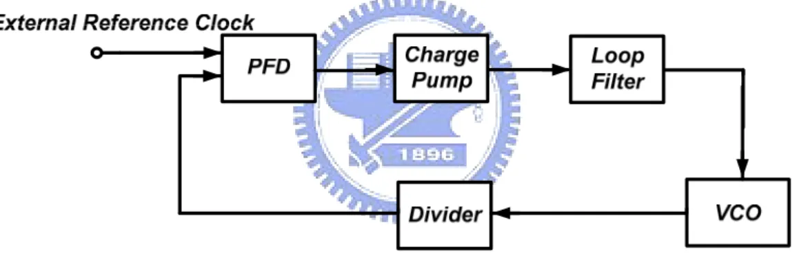
A conventional PLL [13] [3] is composed of a phase frequency detector, a charge pump, a loop filter, a voltage-controlled oscillator and a divider. The typical PLL model is shown in Fig. 2.1:
A 1.25 GB/s Burst-Mode Clock and Data Recovery Circuit with Jitter Reduction Technique
2.1.2 Burst-Mode Clock and Data Recovery Circuit
GVCO-based CDR can be seen in many fast locking applications such as GPON. The architecture of traditional one is proposed in ref. [10], [11] and is shown in Fig. 2.2.
Figure 2.2 Traditional structure of BMCDR Circuit [10][11]
The structure adopts three GVCOs which all operate at the same frequency which is input data rate. Through this structure, although it is very fast locking, however, the three GVCOs must be adopted while run at full rate which consume power very well, as a result, under power consumption consideration, the architecture is phased out.
A better architecture using an edge detector in ref. [1], [2], [8], [12] is adopted lately, which is shown in Fig.2.3. We can observe that only one GVCO in the CDR core is used, moreover, both the GVCOs can even work at half of input data rate [2],
[8]. In other words, through only one half-rate GVCO used in the CDR core, both power and area can be saved. Unfortunately, a requirement of precise half of bit time (Tbit/2) delay in the edge detector is required in such architecture or degrades the jitter
performance [12].
Figure 2.3 Half-Rate Burst-Mode CDR using the edge detector [1], [2], [8], [12]
A 1.25 GB/s Burst-Mode Clock and Data Recovery Circuit with Jitter Reduction Technique
2.2 Design Challenges of Burst-Mode CDR
From previous discussion, we can understand the basics and the operation principal of the Burst-Mode CDR. To be used for several gigabits input data rate of GPON system, there are some design issue in the CDR system, which are:
Locking Time
For GPON applications, the locking bit of the CDR within less than 10 bits is required. Conventional close-loop-based CDR may not be used for these applications. Therefore, open-loop-based CDR architecture is often adopted here.
Jitter
Imprecise value of half of bit time (Tbit/2) delay in the edge detector of open
loop path degrades jitter performance [12]. In practice, however, it is impossible to control the delay time to a value to Tbit/2 exactly due to process
and environmental variation. Therefore, there must be a well controlled mechanism to minimize such jitter generation in the edge detector.
Power
For a CDR with several gigabits per second input data rate, the two GVCOs used in both open loop and close loop path are often required. As a result, large power consumption is inevitable.
2.3 Jitter Issue in Conventional Burst-Mode CDR
The block diagram of a conventional Burst-Mode CDR which adopts an edge detector is shown in Fig. 2.4. To have the best jitter performance of the CDR circuit, the delay in the edge detector must be set to optimum value of half of bit time (Tbit/2)
[12]. However, jitter generation in the open loop path of BMCDR circuits cannot be suppressed effectively by traditional approaches. Generally speaking, the more precise value of half of bit time (Tbit/2) delay in the edge detector is, the better is the jitter
performance.
Figure 2.4 Block diagram of conventional Burst Mode CDR [1], [2], [8], [12]
Let us examine the amount of recovered clock jitter through the simulation results when imprecise value of half of bit time (T /2) delay in the edge detector
A 1.25 GB/s Burst-Mode Clock and Data Recovery Circuit with Jitter Reduction Technique
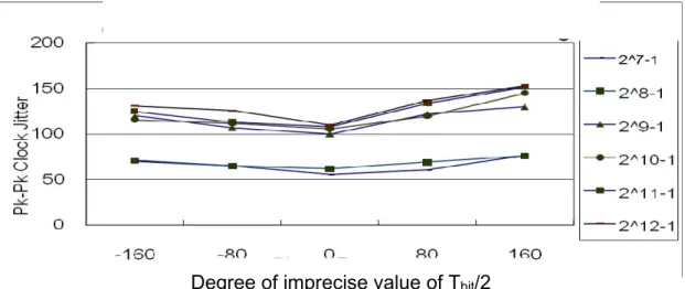
exists. In Fig. 2.5, we can observe that the amount of recovered clock jitter is dominated by two factors; one is the run length of input data while the other one is the degree of imprecise value of Tbit/2.
Figure 2.5 Recovered clock Jitter versus degree of imprecise value of Tbit/2 and
run length of input data.
As a result, there should be a well-controlled tuning mechanism of half of bit time (Tbit/2) delay in the edge detector. Unfortunately, in practice, with temperature
and process variation, it is impossible to control the delay time in edge detector to an optimum value exactly equals Tbit/2. Recently published Burst-Mode CDR papers in
ref. [1], [2], [6] try to use on chip inverter chain or an external chip [12] to realize half-bit time (Tbit/2) delay. However, due to variation of process, these methods may
still result in jitter generation, which also forms jitter in recovered clock. Thus, to ensure minimum jitter generation, an interesting way to produce half of bit time (Tbit/2)
delay precisely in the edge detector is presented in Chapter 3. Degree of imprecise value of Tbit/2
Chapter3
A 1.25 GB/s Burst-Mode Clock and Data
Recovery Circuit with Jitter Reduction Technique
_____________________________________________________________________This chapter starts from the introduction of the system architecture of Burst-Mode CDR with jitter reduction feature. After going through the introduction of system operation principal, we will see the details of every building block used in this design. Finally, the whole system simulation results are interpreted.
3.1 System Architecture
Half rate architecture of the burst-mode CDR circuit developed in ref. [8] is adopted in this work to realize jitter reduction, as shown in Fig. 3.1. The operation principal is similar to the traditional half-rate one with edge detector which is introduced in chapter 2. This architecture not only saves chip area but also consumes less power.
A 1.25 GB/s Burst-Mode Clock and Data Recovery Circuit with Jitter Reduction Technique
3.2 Methodology for Jitter Reduction
The edge detector adopted here is developed in ref. [8] and is used to combine with the proposed half of bit time (Tbit/2) delay generating circuit to produce accurate
half of bit time (Tbit/2) delay in the edge detector. The edge detector circuit is
illustrated in Fig.3.2. The half of bit time (Tbit/2) delay generating circuit, as shown in
Fig. 3.3, is adopted in the edge detector.
To produce half of bit time (Tbit/2) delay in the edge detector, recently published
Burst-Mode CDR papers use on chip inverter chain to realize in ref. [1], [2], [6] or utilize an external chip to switch between just two delays to generate half of bit time (Tbit/2) delay in ref. [12]. However, these methods that produce the delay [1], [2], [6]
or the average delay [12] is still not necessarily falls exactly on Tbit/2 due to process
variation. It will results in jitter generation, too. In this work, differing from ref. [12], a concept that many delays (more than 2) can be chosen and then being “weighted average” to produce half of bit time (Tbit/2) delay is proposed, that is, through
switching between them with unequal weighting factor producing a delay that equals exactly to half of bit time (Tbit/2) delay. The purpose is to further reduce jitter in the
time domain by suppressing harmonic tone in the frequency domain resulting from switching between only two delays periodically. In the design, four delays that are nearest to optimum delay of Tbit/2 result in minimum recovered clock jitter are chosen
and then to be alternatively switched between each other and through weighted average to create a delay that fall exactly on Tbit/2. By post layout simulation, the
recovered clock jitter has better jitter performance when switching between four delays than switching between only two delays that also result in exactly Tbit/2
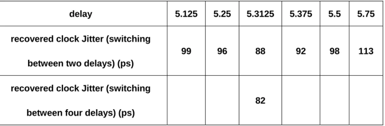
recovered clock jitter. Table 3.2 shows the delays produced by switching between delays that are nearest to Tbit/2 through “weighted average” method and their relative
recovered clock jitter.
Figure 3.2 (a) The rising edge detector [8] with proposed Tbit /2 delay generating
circuit and (b) falling edge detector [8] with Tbit /2 delay generating circuit
Figure 3.3 Tbit /2 delay generating circuit.
Table 3.1 The delay and their relative recovered clock jitter
delay 4 5 6 7 8
A 1.25 GB/s Burst-Mode Clock and Data Recovery Circuit with Jitter Reduction Technique
Table 3.2 The delay and their relative recovered clock jitter.
delay 5.125 5.25 5.3125 5.375 5.5 5.75
recovered clock Jitter (switching between two delays) (ps)
99 96 88 92 98 113
recovered clock Jitter (switching between four delays) (ps)
3.3 Circuit Description
In this section, each circuit block composing the whole burst-mode clock and data recovery circuit is introduced and the simulation results of each block and the whole system simulation results are addressed, too.
3.3.1 Phase-Lock-Loop
The PLL is composed of a phase frequency detector, a charge pump, a loop filter, a voltage-controlled oscillator, and a divider. The PLL with second-order loop filter is chosen in this design as shown in Fig. 3.4.
Figure 3.4 Architecture of the PLL
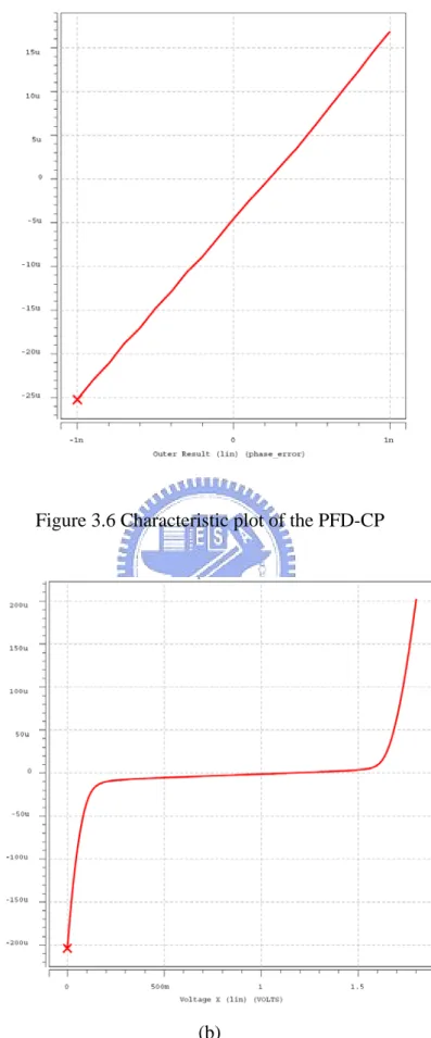
The phase frequency detector of the PLL adopted here is proposed in ref. [14] is shown in Fig. 3.5. The simulation results of the PFD with charge pump is illustrated in Fig.3.6 and the simulation result of charge pump current mismatch is shown in Fig. 3.7. The divide-by-5 divider developed in ref. [15] is used here and the simulation result is shown in Fig. 3.8.
A 1.25 GB/s Burst-Mode Clock and Data Recovery Circuit with Jitter Reduction Technique
(a)
(b)
Figure 3.6 Characteristic plot of the PFD-CP
A 1.25 GB/s Burst-Mode Clock and Data Recovery Circuit with Jitter Reduction Technique
(a)
(b)
Figure 3.8 (a) Schematic [15] and (b) simulation result of the divide-by-5 divider
The phase margin of this PLL is designed larger enough for the system stability consideration in this design. While the ring VCO adopted here is developed in ref. [20] which consists of two delay cells for power saving and the delay cell is shown in Fig. 3.9.
Figure 3.9 Circuit implementation of the delay cell of the ring oscillator. [20]
To reduce the VCO gain, a bias circuit introduced in ref. [22] is shown in Fig. 3.10. It is adopted here to reduce the VCO gain. The simulation result of the overall tuning curve of the VCO under FF, TT, SS corner is shown in Fig. 3.11.
A 1.25 GB/s Burst-Mode Clock and Data Recovery Circuit with Jitter Reduction Technique
Figure 3.11 Simulation result of the two stage ring VCO with the bias circuit.
3.3.2 Clock Recovery Circuit (CRC)
The CRC adopted here is proposed in [8], which is with the features of low power consumption and instantaneous clock recovering. Fig. 3.12 shows the schematic of the CRC while Fig. 3.13 shows the simulation result of the CRC.
Figure 3.12 Circuit implementation of the CRC [8] Input Data Recovered Clock Recovered Data1 Recovered Data2
A 1.25 GB/s Burst-Mode Clock and Data Recovery Circuit with Jitter Reduction Technique
3.3.3 Decision Circuit
The decision circuit is composed of current-mode logic circuit due to its high speed advantages while large power consumption is inevitable. The current-mode DFF developed in ref. [21] is used here, as shown in Fig. 3.14.
3. 4 Whole System Simulation Results
Through the matlab simulink behavior model of PLL, the transient response of the PLL is simulated. Fig. 3.15 and Fig. 3.16 illustrate the behavior level transient response and frequency response of the PLL. Fig. 3.17 shows the post layout simulation of transistor level transient response of PLL.
Figure 3.15 Behavior level transient response of PLL.
A 1.25 GB/s Burst-Mode Clock and Data Recovery Circuit with Jitter Reduction Technique
Figure 3.17 Transistor level transient response simulation result of PLL.
After PLL is locked, a test pattern of 1.25-Gb/s PRBS is sent to the CDR. The waveforms are shown in Fig. 3.18, including input data, the control voltage on the PLL, recovered clock, and two recovered data sequences.
Vctrl Input Data Recovered Clock Recovered Data2 Recovered Data1
A 1.25 GB/s Burst-Mode Clock and Data Recovery Circuit with Jitter Reduction Technique
Figure 3.18 Recovered clock and recovered data from the CDR circuit
Fig. 3.19(a) shows the jitter histogram of the recovered clock, and Fig. 3.19(b) illustrates eye diagram of the retimed data. The recovered data eye diagram shows the Burst-Mode CDR with jitter reduction features meet the jitter mask of GPON specification. The total power consumption of the CDR is 32.1mW. Finally, table 3.3 gives the performance summary of the burst-mode CDR.
Recovered Data1 Recovered Data2 Recovered Clock Input Data Vctrl
A 1.25 GB/s Burst-Mode Clock and Data Recovery Circuit with Jitter Reduction Technique
(b)
Figure 3.19(a) the jitter histogram of the recovered clock, and (b) the jitter histograms of the retimed data.
Table 3.3 Performance summary.
Pre‐SIM Post‐SIM
Technology
0.18µm CMOS 0.18µm CMOSInput data
Rate
1.25Gb/s 1.25Gb/sSupply Voltage
1.8v 1.8vLocking time
1 bit(0.8ns) 1 bit(0.8ns)Power
31.93mW 32.1mWJitter
Performance
Recovered clock (jitter reduction technique is disable): 59ps (PK‐PK) Recovered clock (jitter reduction technique is active): 53ps (PK‐PK) Retimed data: 32ps (PK‐PK) Recovered clock (jitter reduction technique is disable): 105ps (PK‐PK) Recovered clock (jitter reduction technique is active): 82ps (PK‐PK) Retimed data: 72ps (PK‐PK)Experimental Result
Chapter 4
Experimental Result
This chapter starts from the introduction of the chip information and then the measurement environment is presented. In the end of this chapter, the experimental results will be interpreted.
4.1 Chip Information
The burst-mode clock and data recovery circuit with an on-chip jitter reduction circuit is fabricated through National Chip Implementation Center in TSMC CMOS 0.18-μm technology. Fig. 4.1(a) shows the layout and Fig. 4.1(b) illustrates the die photo. The area is 0.99×0.97 mm2
.
(b)
Experimental Result
4.2 Measurement Consideration
4.2.1 Printed Circuit Board
Fig. 4.2 shows the photograph of the chip with the PCB. The chip is measured under 1.8v power supply.
Fig.4.2 The top view of PCB.
4.2.2 Measurement Environment Setup
Fig. 4.3 shows the setup for measurement. It is worth to mention that each digital control signal is generated by Acute PG 2050 controlled by a PC.
Experimental Result
4.3 Experimental Result
When data stream is sent to the chip, we first measure the recovered clock jitter of the delays that are nearest to Tbit/2. From the simulation results, we know that the
more precise value of half of bit time (Tbit/2) delay in the edge detector is; the better is
the jitter performance. Base on the result, we found 4 delays in the delay line that have less recovered clock jitter, which are delay 4, delay 5, delay 6, and delay 7, the corresponding recovered clock jitter are 160ps, 150ps, 130ps, 175ps, respectively, as Table 4.1 shows. If we choose the delay that is too far away from Tbit/2, in this case,
delay 11, the recovered clock jitter would be extremely large as shown in Fig. 4.4.
Table 4.1 The delay and corresponding recovered clock jitter
delay 4 5 6 7 11
P-P Jitter(ps) 160 150 130 175 310
Figure 4.4 Measurement results of recovered clock jitter based on different delay time.
Second, we try to find the probably location of Tbit/2. Due to have less recovered
clock jitter of delay 5 and 6, we can judge that Tbit/2 must fall between the two delays,
and then, a stream of random pattern that generates delay of 5.5 is sent to the chip; the measured recovered clock jitter (peak-peak) is 123.5ps at 540MHz, as shown in Fig.4.5. After that, two random patterns that generates delay of 5.333 and 5.667 are sent to the chip, the measured recovered clock jitter (peak-peak) are 124.0ps at 540MHz and 121.2ps at 540MHz, respectively, which are shown in Fig. 4.6 and Fig. 4.7. We can observe that the Tbit/2 may fall between delay 5.667 and 6, and then, two
random patterns that generates delay of 5.7 and 5.78 are sent to the chip, the measured recovered clock jitter (peak-peak) are 116.5ps at 540MHz and 114.3ps at 540MHz, respectively, which are shown in Fig. 4.9 and Fig. 4.10. Table 4.2 illustrates the relationship between delay and recovered clock jitter. Generally speaking, the more precise value of half of bit time (Tbit/2) delay is, the better is the jitter performance.
Experimental Result
Figure 4.5 When delay is 5.5, the recovered clock jitter (peak-peak) is 123.5ps at 540MHz
Figure 4.6 When delay is 5.33, the recovered clock jitter (peak-peak) is 124.0ps at 540MHz
Figure 4.7 When delay is 5.66, the recovered clock jitter (peak-peak) is 121.2ps at 540MHz
Figure 4.8 When delay is 5.68, the recovered clock jitter (peak-peak) is 118.8ps at 540MHz
Figure 4.9 When delay is 5.7, the recovered clock jitter (peak-peak) is 116.5ps at 540MHz
Experimental Result
Table 4.2 The relationship between delay and recovered clock jitter Clock Jitter v.s. Average Delay Value
0 100 200
5 5.33 5.5 5.66 5.68 5.7 5.78 6
Average Delay Value
R eco ve re d C lo ck Ji tte r Clock Jitter v.s. Average Delay Value
4.4 Experimental Results Summary
The measurement results of recovered clock jitter show the more precise value of Tbit/2 is, the better is the jitter performance. When probably position of Tbit/2 is found,
a calibration pattern can be fed into Tbit/2 delay generating circuit to calibrate
recovered clock jitter. The recovered data is not available due to my careless layout about current density (2.5mA/0.22μm) which results in burning in metal line of output DFF. Fig. 4.11 shows the die photo of the decision circuit, which illustrates the metal line was burned, thus, the DFF cannot work properly. Table 4.3 shows the comparison between pre-layout simulation, post-layout simulation, and measurement results of the Burst-Mode CDR circuit. The results all illustrate significant jitter reducing when jitter reduction technique is enable.
Experimental Result
Table 4.3 Burst-Mode CDR performance summary
Pre‐SIM Post‐SIM(1) Post‐SIM(2) Measurement
Technology
0.18µm CMOS 0.18µm CMOS 0.18µm CMOS 0.18µm CMOSInput data
Rate
1.25Gb/s 1.25Gb/s 1.08Gb/s 1.08Gb/sSupply
Voltage
1.8v 1.8v 1.8v 1.8VLocking time
1 bit(0.8ns) 1 bit(0.8ns) 1 bit(0.8ns) N/APower
31.93mW 32.1mW 30.6mW 36mWJitter
Performance
Recovered clock (jitter reduction technique is disable): 59ps (PK‐PK) Recovered clock (jitter reduction technique is enable): 53ps (PK‐PK) Retimed data: 32ps (PK‐PK) Recovered clock (jitter reduction technique is disable): 105ps (PK‐PK) Recovered clock (jitter reduction technique is enable): 82ps (PK‐PK) Retimed data: 72ps (PK‐PK) Recovered clock (jitter reduction technique is disable): 92ps (PK‐PK) Recovered clock (jitter reduction technique is enable): 77ps (PK‐PK) Retimed data: 61ps (PK‐PK) Recovered clock (jitter reduction technique is disable): 130ps (PK‐PK) Recovered clock (jitter reduction technique is enable): 114.3ps (PK‐PK) Retimed data: N/A4.5 Performance Comparison
Table 4.4 shows the comparison of the burst-mode clock and data recovery circuit.
Table 4.4 Burst-Mode Clock and Data Recovery performance comparison
[6]
[5]
[12]
This Work
Technology
0.18µm CMOS 0.18µm CMOS 0.35µm CMOS 0.18µm CMOSInput data
Rate
1.25Gb/s 2.5Gb/s 155.52Mb/s 622.08Mb/s 1244.16Mb/s 2488.32Mb/s 155Mbps 1.08Gb/sChip Area
N/A 1.5mm² 2.1x2.1mm² 1mm²Supply
Voltage
1.8 1.8 3.3 1.8Locking time
1 bit 6 bit N/A N/APower
60mW for core 50mW for output buffer 70mW N/A 36mWJitter
Performance
Recovered clock: 108ps (PK‐PK) Retimed data: 98.8ps (PK‐PK) Recovered clock: 115.16ps (PK‐PK) Retimed data: N/A Recovered clock: 416ps (PK‐PK) Retimed data: N/A Recovered clock: 114.3ps (PK‐PK) Retimed data: N/AConclusion and Future Works
Chapter 5
Conclusion and Future Works
5.1 Conclusion
In this thesis, a Burst-Mode CDR with jitter reduction technique is presented. The design challenges of this design is discussed and solved. This work integrates a Tbit /2
delay generating circuit into the burst-mode CDR chip to realize jitter reduction.
The measurement results show that the more precise value of half of bit time (Tbit/2) delay in the edge detector, the better is jitter performance. When jitter
reduction technique is disabling, the measured recovered clock jitter is 130ps, while the jitter reduction technique is enable, the measured recovered clock jitter is 114.3ps, reduced by 13.7%. When probably position of Tbit/2 is found, a calibration pattern can
be fed into Tbit /2 delay generating circuit to calibrate recovered clock jitter. The chip
size is 0.99 0.97 mm². The power consumption of the CDR is 36mW under 1.8V power supply. The designed Burst-Mode CDR is fabricated in TSMC 0.18 μm 1P6M CMOS process.
5.2 Future Works
This work introduces the idea that the more precise value of half of bit time (Tbit/2) delay in the edge detector is, the better is the jitter performance. From the
experimental results, a feedback circuit used for detecting the location of Tbit/2
position can be added in the future work to produce calibration pattern automatically, and then calibrate the recover clock jitter.
Recently published Burst-Mode CDR related papers operates up to 10 gigabit/s. Therefore, higher operation frequency of Burst-Mode CDR must be developed. The calibration scheme of the jitter reduction circuit would also be useful by replacing the static logic circuits in Tbit /2 delay generating circuit with current mode logic circuits
for better resolution.
Finally, the divider of the Burst-Mode CDR can be further improved to satisfy all the input data rate operation of GPON specification.
Bibliography
Bibliography
[1] M. Nogawa, K.Nishimura, S. Kimura,Yoshida, T.Kawamura, M.Togashi, K. Kumozaki, and Y.Ohtomo, “A 10Gb/s burst-mode CDR IC in 0.13um CMOS,” IEEE International Solid-State Circuits Conference, pp.228-229, Feb. 2005. [2] Yu-Gun Kim, Chun-Oh Lee, Seung-Woo Lee, Hyun-Su Chai, Hyun-Suk Ryu,
Woo-Young Choi, “Novel 622Mb/s Burst-Mode Clock and Data Recovery Circuits with Muxed Oscillators,"IEICE Trans. Commun., vol. E86-B, no. 11,pp.3288-3292, Nov. 2003.
[3] S. I. Liu and C. Y Yang, Phase-Locked Loops, Tsang-Hai, 2006.
[4] “G.984.2 Gigabit-capable passive optical networks (GPON): Physical media dependent (PMD) layer specification,” ITU-T, 2003.
[5] Che-Fu Liang, Sy-Chyuan Hwu, Shen-Iuan Liu, ” A Multi-Band Burst-Mode Clock and Data Recovery Circuit “IEICE Trans. Electron., vol.E90–C, no.4, April 2007
[6] Han, P.-S.; Choi, W.-Y, " 1.25/2.5-Gb/s Dual Bit-Rate Burst-Mode Clock Recovery Circuits in 0.18um-CMOS Technology, ” IEEE Transactions on Circuits and Systems II-Express Briefs, vol. 54, no. 1, Jan. 2007.
[7] J.-H. Weng, M.-T. Tasi, J.-M. Lin, and C.-Y. Yang, “A 1.8-Gb/s burst mode clock and data recovery circuit with a 1/4-rate clock technique,” IEEE International Symposium Circuits and Systems, pp.-3076, May 2006.
[8] Ching-Yuan Yang, and Jung-Mao Lin, “A 1.25-Gb/s Burst-Mode Half-Rate Clock and Data Recovery Circuit Using Realigned Oscillation,” IEICE Trans. Electron., vol.E90–C, no.1 Jan. 2007 .
[9] A. E. Dunlop, W. C. Fischer, M. Banu, and T. Gabara, “150/30 Mb/s CMOS non-oversampled clock and data recovery circuits with instantaneous locking and jitter rejection,” IEEE International Solid-State Circuits Conference, pp. 44-45, Feb. 1995.
[10] M. Banu, and A. E. Dunlop,”A 660 Mb/s CMOS clock recovery circuit with instantaneous locking for NRZ data and burst-mode transmission,” IEEE International Solid-State Circuits Conference, pp. 102-103, Feb.1995.
[11] Y. Ota, R. G. Swartz, M. Banu, A. E. Dunlop, “High-Speed, Burst-Mode, Packet-Capable Optical Receiver and Instantaneous Clock Recovery for Optical Bus Operation," IEEE Journal of Lightwave Technology, vol. 12, no.2, pp. 325-331, Feb. 1994.
[12] J.-S. Hwang, C.-S. Park, and C.-S. Park, “155-Mb/s burst-mode clock recovery circuit using the jitter reduction technique,” IEICE Trans., vol.E86, pp.1423–1426, April 2003.
[13] R. E. Best, Phase-Locked Loops: theory, design and applications, 5th edition, New York: McGraw-Hill, 2003.
[14] A. Chandrakasan, W. J. Bowhill, and Fox, Design of High-Performance Microprocessor Circuit, IEEE Press, 2001 , p. 240
[15] C. Y. Yang, G. K. Dehng, J. M. Hsu and S. I. Liu, “New dynamic flip-flops for high-speed dual-modulus prescaler ”, IEEE J. Solid-State Circuits, vol. 33, no. 10, pp. 1568-1571, Oct. 1998.
[16] Jung-Mao LIN, “Inplementation of 0.18-um Burst-Mode Clock and Data Recovery Circuits for Passive Optical Networks,” Master Thesis, National Chung-Hsing University, 2006.
Bibliography
[18] A. Hajimiri and T.H. Lee, “A general theory of phase noise in electrical oscillator,” IEEE J. Solid-State Circuits, vol.33, no.2, pp.179–194, Feb. 1998. [19] S. Ye, L. Jansson, and I. Galton, “A multiple-crystal interface PLL with VCO
realignment to reduce phase noise,” IEEE J. Solid-State Circuits, vol.37, no.12, pp.1795–1803, Dec. 2002.
[20] W.S.T. Yan and H.C. Luong, “A 900-MHz CMOS low-phase-noise voltage-controlled ring oscillator,” IEEE Trans. Circuits Syst. II, vol.48, no.2, pp.216–221, Feb. 2001.
[21] B. Razavi, Design of Integrated Circuits for Optical Communications, McGraw-Hill, 2003.
[22] C. Y Yang, “Design of Clock Synchronizers and Frequency Synthesizers,” University of Taiwan, PhD Thesis, 2000.
[23] B. Razavi, RF Microelectronics, Prentice Hall, Inc. 1998.
[24] Sy-Chyuan Hwu, “Burst-Mode Clock and Data Recovery Circuit for Passive Optical Networks,” Master Thesis, National Taiwan University, 2005.
![Figure 2.3 Half-Rate Burst-Mode CDR using the edge detector [1], [2], [8], [12]](https://thumb-ap.123doks.com/thumbv2/9libinfo/8017732.160691/17.892.154.753.302.721/figure-half-rate-burst-mode-cdr-using-detector.webp)
![Figure 2.4 Block diagram of conventional Burst Mode CDR [1], [2], [8], [12]](https://thumb-ap.123doks.com/thumbv2/9libinfo/8017732.160691/19.892.148.779.513.926/figure-block-diagram-conventional-burst-mode-cdr.webp)
![Figure 3.2 (a) The rising edge detector [8] with proposed T bit /2 delay generating circuit and (b) falling edge detector [8] with T bit /2 delay generating circuit](https://thumb-ap.123doks.com/thumbv2/9libinfo/8017732.160691/23.892.299.594.270.691/figure-detector-proposed-generating-falling-detector-generating-circuit.webp)
![Figure 3.5 (a) PFD schematic [14] and (b) the function](https://thumb-ap.123doks.com/thumbv2/9libinfo/8017732.160691/26.892.197.723.124.1085/figure-pfd-schematic-b-function.webp)
![Figure 3.8 (a) Schematic [15] and (b) simulation result of the divide-by-5 divider](https://thumb-ap.123doks.com/thumbv2/9libinfo/8017732.160691/28.892.192.715.117.756/figure-schematic-b-simulation-result-divide-divider.webp)
![Figure 3.9 Circuit implementation of the delay cell of the ring oscillator. [20]](https://thumb-ap.123doks.com/thumbv2/9libinfo/8017732.160691/29.892.349.545.119.377/figure-circuit-implementation-delay-cell-ring-oscillator.webp)
