Optical investigation of GaSb thin films grown on GaAs by
metalorganic magnetron sputtering
Z.C. Feng
a,⁎
, F.C. Hou
a, J.B. Webb
b, Z.X. Shen
c, E. Rusli
d, I.T. Ferguson
e, W. Lu
fa
Graduate Institute of Electro-Optical Engineering and Department of Electrical Engineering, National Taiwan University, Taipei, 106-17, Taiwan, ROC
b
Institute for Microstructural Sciences, National Research Council Canada, Ottawa, Ontario, Canada K1A 0R6
c
Division of Physics & Applied Physics, School of Physical & Mathematical Sciences, Nanyang Technological University, Singapore 63979, Singapore
d
School of Electrical & Electronic Engineering, Nanyang Technological University, Singapore 63979, Singapore
e
School of Electrical & Computer Engineering, Georgia Institute of Technology, Atlanta, GA 30332-0250, USA
f
Department of Chemistry, Fisk University, Nashville, TN 37208, USA Available online 13 July 2007
Abstract
Metalorganic magnetron sputtering (MOMS) technology has been applied to the growth of epitaxial GaSb layers on GaAs (001). Optical studies are performed on a series of GaSb/GaAs samples grown under different growth conditions. Raman scattering measurements indicated the improvement of the crystalline quality of the GaSb thin film from the interface toward the surface with decreasing substrate growth temperature from 480 °C to 400 °C. Fourier transform infrared (FTIR) reflectance revealed the possible existence of an intermixed GaSb–GaAs layer near the interface. In UV reflectance spectra, the shapes of the high energy transition bands were found to be associated with the GaSb film quality. © 2007 Elsevier B.V. All rights reserved.
Keywords: Metalorganic magnetron sputtering; Raman scattering; FTIR; UV reflectance
1. Introduction
The III–V compound semiconductor gallium antimonide (GaSb) has in recent years attracted much attention as an important material for infrared (IR) optoelectronic and electronic device in the wavelength range 1–5 μm[1–13]. GaSb has an energy bandgap of 0.70 eV (1.77μm) at room temperature (RT) and 0.81 eV (1.53μm) at 4 K[14]. Its lattice constant of 6.0959 Å at RT matches that of various ternary and quaternary compounds with band gaps covering a wide spectral range of 0.3–1.58 eV (0.8–4.3 μm)[11,14]. The GaSb–InAs superlattice (SL) with the type-II band offset structure has shown special electronic properties with useful applications[5,8,9]. Type-II GaInAsSb–
GaSb heterojunctions and other GaSb-based quantum structures have played an important role in recent research and development of high power laser diodes and detectors operating in the mid-IR 2–5 μm region[15,16]. Good epitaxial growth of GaSb on GaAs (001) is important for research and development[11,17]. Due to
the lattice mismatch between GaSb and GaAs (∼7%), epilayers a few microns thick typically possess a high density of dislocations, and therefore, it has been essential to develop techniques to control film quality control and evolution[11,17].
Various growth techniques have been employed in the growth of GaSb on GaAs (001) [[11] and references therein], among which the major methods of molecular beam epitaxy (MBE) and metalorganic vapor phase epitaxy (MOVPE) have been empha-sized in past years. However, new technologies are developing to challenge these two growth methods. The conventional solid sources in MBE can cause problems for the growth of materials with high vapour pressure. To overcome this difficulty, gaseous and metalorganic vapor sources have been added to MBE to achieve a marriage between MBE and MOVPE. This new growth technique, called metalorganic molecular beam epitaxy (MOMBE)[18]or chemical beam epitaxy (CBE)[19], combines the advantages of MBE and MOVPE, providing stable group V vapor beams for epitaxy. In another approach, we have developed a novel technology of metalorganic magnetron sputtering (MOMS) for the preparation of epitaxial InSb and Sb-based materials and microstructures[20–23]. Pulsed laser evaporation and epitaxy (PLEE) is another method, which avoids the use of
Thin Solid Films 516 (2008) 5493–5497
www.elsevier.com/locate/tsf
⁎ Corresponding author.
E-mail address:[email protected](Z.C. Feng).
0040-6090/$ - see front matter © 2007 Elsevier B.V. All rights reserved. doi:10.1016/j.tsf.2007.07.049
the thermal or vapor sources [24]. Clearly, no single growth technique can hope to achieve optimal results for all materials systems. New techniques are being pursued to combine the advantages of various growth methods.
In this paper, we report on the epitaxial growth and optical characterization of GaSb thin films (less than 1 μm thick) on GaAs (001) via MOMS. Usually, MBE growth of GaSb on GaAs (001) is performed in the temperature range of 500–600 °C[11], or lower, at 490 °C[17]. For the MOVPE growth of GaSb on GaAs (001), different temperature ranges were used, such as 560– 620 °C[25]and 400–560 °C[26]. In our MOMS growth process, lower substrate growth temperatures were employed and an optimum temperature was found to be close to 400 °C. Detailed results of the optical characterization for MOMS grown GaSb on GaAs (001) in the temperature range 400–480 °C are presented. 2. Experiment
2.1. Sample preparation
The MOMS deposition system consists of an ultra-high-vacuum (UHV) chamber with sample load-lock and planar magnetron sputter guns. The UHV system was cryogenically pumped to a base pressure of∼10− 7Pa before deposition. The GaAs substrates were cleaned using a (H2SO4:H2O2:H2O = 6:1:1)
wet etch. Substrates were thermally bonded to an indirectly heated molybdenum holder using indium solder. The substrate temper-ature was monitored with a calibrated thermo-couple in close proximity to the rotating holder. DC reactive sputtering of high-purity polycrystalline Sb target was performed in the presence of metalorganic vapors of trimethylgallium (TMG). The TMG bubbler was held at 0 °C. The getter-purified high-purity argon was introduced via a mass-flow controller to serve as the carrier gas to control the TMG flow rate. The total gas flow rate was maintained at 30 sccm under a low deposition pressure of ∼0.4 Pa. All growths were carried out in an antimony stabilized regime[20–23].
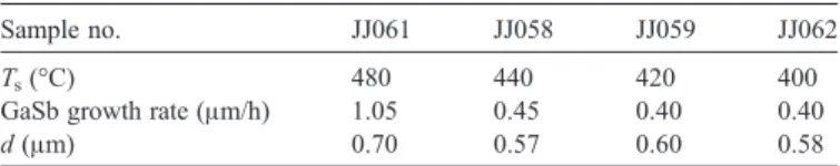
In the present study, thin (0.5–0.7 μm) GaSb films were grown on GaAs (001) substrate with different substrate growth temperature, TS, between 400 and 480 °C. These led to different
growth rates as listed inTable 1. Starting from a high TS= 480 °C, a
growth rate of slightly higher than 1μm/h was obtained. At higher TS, the thermal decomposition of metalorganic dominates. When
TSdecreases, the thermal cracking of metalorganic is reduced and
plasma induced decomposition of metalorganic becomes the dominant process, leading to a decrease of the growth rate. When TSis lower than 430 °C the growth rate was saturated at a low rate
of 0.40μm/h[27]indicating the over- through domination of the
plasma induced decomposition mechanism. After the growth, these experimental samples were examined by X-ray diffraction (XRD), scanning electron microscopy (SEM), Hall and optical absorption measurements[27].
2.2. Materials characterization techniques
In this paper Raman scattering, UV–Visible optical reflec-tance and Fourier transform infrared (FTIR) spectroscopy were employed to further investigate the material properties of MOMS grown GaSb on GaAs (001) and their dependence on substrate growth temperature.
Raman scattering was measured in the near back-scattering geometry with samples held at a low temperature dewar (80 K), or RT, and excited by an Ar+ laser with a focused spot size b0.3 mm. The scattered light was dispersed by a triple spectrometer and detected by a sensitive optical multichannel analyzer with resolutions of 2–3 cm− 1[28]. Fourier transform
infrared (FTIR) reflectivity measurements in the wavenumber range of 20–250 or 20–500 cm− 1 were done using a Grubb– Parsons Fourier spectrometer with a Golay detector, at temperatures of 300 and 80 K. The reflection coefficient was determined as the ratio of the intensity of the light reflected from the sample against that reflected from a reference mirror made of coin silver with about 98% reflectance [21]. Optical reflectance was measured using a Hitachi U-3410 spectropho-tometer in the wavelength range between 190 and 2500 nm. 3. Results and discussion
3.1. Raman scattering
Fig. 1shows comparative RT Raman spectra of three MOMS
grown GaSb/GaAs (001) and a bulk GaSb. The GaSb longitudinal
Table 1
Sample information
Sample no. JJ061 JJ058 JJ059 JJ062
Ts(°C) 480 440 420 400
GaSb growth rate (μm/h) 1.05 0.45 0.40 0.40
d (μm) 0.70 0.57 0.60 0.58
Ts: substrate growth temperature (°C).
d: GaSb film thickness (μm).
Fig. 1. Raman spectra from three MOMS-grown GaSb/GaAs (001) grown at substrate temperature of (a) 480 °C, (b) 440 °C and (c) 400 °C, and (d) a bulk GaSb.
optical (LO) and transverse optical (TO) phonon mode at the center of Brillioun zone were detected. According to Raman selection rules, the LO phonon mode is allowed and TO is forbidden for the (001) orientation of a zincblende crystal[28].
Because these GaSb films are thinner than 0.6μm, there exist a high density of dislocations in the films[17], which breaks the symmetry and leads to the appearance of the forbidden TO modes. The LO and TO modes can be distinguished by polarization measurements as shown inFig. 2, where X is along the (100) axis and X is its reversed direction, Y′ is along (011) and Z′ is along (011). Obeying the selection rule for a (100) surface from a zincblende crystal[28], the LO mode is allowed in the X(Y′Y′) X configuration and forbidden in X(Y′Z′)X, while the TO mode is allowed in X(Y′Z′)X and forbidden in X(Y'Y')X, which confirms the assignments for LO and TO modes. The mode appeared at 195 cm− 1 in X(Y′Z′)X may be due to the defect activated longitudinal optical (DALO) phonon, related to defects in the sample.
As seen inFig. 1(a), the“forbidden” TO mode is dominant for samples grown at Ts= 480 °C. As Tsdecreases to 440 °C, in
Fig. 1(b), the LO mode intensity increases with respect to the
TO mode. At Ts= 400 °C, the allowed LO mode is dominant
with a weak shoulder, “forbidden” TO mode, Fig. 1(c). This indicates that the film quality improves with decreasing substrate growth temperature, which is consistent to the XRD result showing a narrowing of the (004) GaSb peak as decreasing Ts (data not shown here). But, we found that we
could not grow an epitaxial film for Tsb400 °C. Therefore, the
optimum substrate temperature for growth of epitaxial GaSb thin films using the MOMS technique is about 400 °C.
Fig. 3 shows Raman spectra from a MOMS-grown GaSb/
GaAs sample made at a high substrate temperature 480 °C, measured under different excitation wavelengths between 4579 and 5017 Å from an Ar+ laser. As seen, with decreasing excitation wavelength or penetration depth fromFig. 3(f) to (a),
Fig. 3. Raman spectra from a MOMS-grown GaSb on GaAs (100) with Ts= 480 °C, under different excitation wavelengths between 4579 and 5017 Å
from an Ar+laser.
Fig. 2. Raman spectra from a MOMS-grown GaSb/GaAs (100) with Ts= 400 °C, measured under different polarization configurations: (a) no
po-larization, (b) X(Y′Y′)X and (c) X(Y′Z′)X.
Fig. 4. FTIR reflectivity spectra from four MOMS-grown GaSb/GaAs (100) under different substrate growth temperature of (a) 400 °C, (b) 420 °C, (c) 440 °C and (d) 480 °C.
the forbidden TO mode decreases in intensity with respect to the allowed LO mode, indicating the development of the crystalline perfect towards the surface.
3.2. FTIR reflectance and interface mode
Because visible laser light penetrates only tens of nanometer into GaSb, Raman scattering cannot probe the GaSb/GaAs interface directly. Instead, we used infrared light which can penetrate the entire GaSb layer to probe the GaSb/GaAs interface.Fig. 4exhibits FTIR reflectivity spectra for this series of MOMS-grown GaSb/GaAs at different Ts. There exist two
major bands, one of near 270 cm− 1 due to the TO phonon vibration from GaAs substrate [29] and another one of near 230 cm− 1from the TO mode of GaSb film[21,29]. In addition, a third mode appears at about 254 cm− 1 between these two major bands and develops with increasing Ts. This third mode
might be due to the existence of a GaAs–GaSb intermixed layer near the interface. It was varied with Ts. Further study on this
mode is needed.
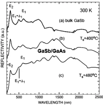
3.3. UV–VIS–NIR optical reflectance
Optical reflectance spectra covering the ultraviolet to near-infrared range 200–2500 nm have also been used to evaluate the GaSb/GaAs samples, as displayed in Fig. 5, for two of our MOMS-grown samples and from a wafer of bulk GaSb, shown for comparison. The three reflectivity maxima between 200 and 700 nm represent the high energy GaSb E1, E1+Δ1 and E2
band gaps. These peaks display similar heights and half-widths for the bulk sample and the epitaxial sample grown at 400 °C. But they become flatter and less-well defined for the sample grown at 480 °C. This can also be taken as an indication of lower sample quality at the higher growth temperature,
consistent with our Raman and FTIR results. This might also be related to the poorer surface roughness from the sample grown at higher temperature. The UV–VIS–NIR optical reflectivity spectra for GaSb/GaAs also exhibit some interfer-ence fringes in the wavelength range beyond 1000 nm. These can also be used to determine the GaSb film thickness. The results are given inTable 1, which are consistent with the data obtained from scanning electron microscope (SEM) measure-ments by examining a cleaved edge[29].
4. Conclusion
Metalorganic magnetron sputtering (MOMS) technology has been applied to the growth of epitaxial thin GaSb layers on GaAs (100) with the film thickness less than 0.6μm. Optical characterization has been performed on a series of GaSb/GaAs epilayers grown under different conditions. The following significant results are obtained:
Raman scattering on MOMS-grown GaSb/GaAs (100) shows that the forbidden TO mode is dominant for the sample grown at high substrate growth temperature (480 °C). Its intensity with respect to the allowed LO phonon mode decreases with decreasing Tsfrom 480 °C to 400 °C. At Tsof
400 °C, the LO mode dominates the spectrum. The TO appears as a weak shoulder and this occurs because of defects induced by lattice mismatch in these films much thinner than 1μm.
Raman scattering indicates directly and clearly that the GaSb film quality improves with decreasing substrate growth temperature from 480 °C to 400 °C.
Raman scattering with different laser excitation wavelengths indicates that the crystalline perfection of the GaSb thin film improves with vertical distance away from the interface and toward the surface.
The MOMS technique yields an optimum substrate growth temperature of ∼400 °C, which is lower than the growth temperature used in MBE and MOCVD techniques.
A new mode near 254 cm− 1between the GaSb and GaAs TO modes was observed from FTIR reflectance, which might be related to the GaSb–GaAs intermixed layer near the interface.
Growth at high temperature damps the E1 and E1+Δ1
electronic transition bands in the ultraviolet, and UV reflectance spectra can be used to monitor GaSb film quality. Interference fringes in the near infrared can be used to determine the film thicknesses.
These results on MOMO-grown GaSb/GaAs will enhance our efforts in developing the MOMS technique for materials growth and help us understand both the growth mechanisms and the physics of these hetero-structures for IR applications. Further penetrative and qualitative analysis on Raman and IR spectra and correlation with SEM and XRD data will be made in the near future.
Acknowledgements
We acknowledge the help and supports from Profs. S. Perkowitz and S. H. Tang. The work was supported by funds at National Taiwan University from National Science Council of
Fig. 5. UV–IR optical reflectivity spectra from (a) bulk GaSb wafer and MOMS-grown GaSb/GaAs samples MOMS-grown at (b) Ts= 400 °C and (c) Ts= 480 °C.
Republic of China, NSC 94-2215-E-002-019 and 95-2221-E-002-118, and at Fisk University by the NSF (Grant No: HRD-0420516) Center for Physics and Chemistry of Materials. References
[1] Hyunjung Kim, E. Tarhan, G. Chen, A.K. Ramdas, M. Dean Sciacca, R.L. Gunshor, Semicond. Sci. Technol. 21 (2006) 1224.
[2] D. Kindl, P. Hubík, J. Krištofik, J.J. Mareš, E. Hulicius, J. Pangrác, K. Melichar, Z.V. Výborný, J. Touškov´, Semicond. Sci. Technol. 21 (2006) 180.
[3] O. Vigil-Galán, J.N. Ximello-Quiebras, J. Aguilar-Hernández, Gerardo Contreras-Puente, A. Cruz-Orea, J.G. Mendoza-Álvarez, J.A. Cardona-Bedoya, C.M. Ruiz, V. Bermúdez, Semicond. Sci. Technol. 21 (2006) 76. [4] S.M. Kluth, J.D. Fitz Gerald, M.C. Ridgway, Appl. Phys. Lett. 86 (2006)
131920.
[5] Jian V. Li, Shun Lien Chuang, Eric M. Jackson, Edward Aifer, Appl. Phys. Lett. 85 (2004) 1984.
[6] M.P. Hanson, D.C. Driscoll, J.D. Zimmerman, A.C. Gossard, E.R. Brown, Appl. Phys. Lett. 85 (2004) 3110.
[7] Z.Y. Liu, D.A. Saulys, T.F. Kuech, Appl. Phys. Lett. 85 (2004) 4391. [8] H.J. Haugan, F. Szmulowicz, G.J. Brown, K. Mahalingam, Appl. Phys.
Lett. 84 (2004) 5410.
[9] Y. Wei, A. Gin, M. Razeghi, G.J. Brown, Appl. Phys. Lett. 80 (2002) 5410. [10] F.M. Liu, L.D. Zhang, Semicond. Sci. Techol. 14 (1999) 710.
[11] P.S. Dutta, H.L. Bhat, V. Kumar, J. Appl. Phys. 81 (1997) 5821. [12] A. Bignazzi, A. Bosacchi, R. Magnanini, J. Appl. Phys. 81 (1997) 7540. [13] M. Gauneau, R. Chaplain, A. Rupert, Y. Toudic, R. Callec, J. Appl. Phys.
73 (1993) 2051.
[14] V. Swaminathan, A.T. Macrander, Materials Aspects of GaAs and InP Based Structures, Prentice Hall, New Jersey, 1991.
[15] M.P. Mikhailova, A.N. Titkov, Semicond. Sci. Technol. 9 (1994) 1279. [16] G.W. Turner, H.K. Choi, M.J. Manfra, M.K. Connors, in: M.O. Manasreh,
T.H. Myers, F.H. Julien (Eds.), Infrared Applications of Semiconductors-Materials, Processing and Devices, Mat. Res. Soc. Symp. Proc., vol. 450, Materials Research Society, Pittsburgh, 1997, pp. 3–12.
[17] P.M. Thibado, B.R. Bennett, M.E. Twigg, B.V. Shanabrook, L.J. Whitman, J. Vac. Sci. Technol., A 14 (1996) 885.
[18] W. Zhou, K. Uesugi, I. Suemune, Appl. Phys. Lett. 83 (2003) 1992. [19] J.O. Maclean, T. Martin, M.R. Houlton, P.D.J. Calcott, S.G. Ayling, K.P.
Hilton, S.A. Rushworth, L.M. Smith, Appl. Phys. Lett. 80 (2002) 914. [20] J.B. Webb, R. Rousina, in: Z.C. Feng (Ed.), Semiconductor Interfaces and
Microstructures, World Scientific Publishing, Singapore, 1992, p. 199. [21] M. Macler, Z.C. Feng, S. Perkowitz, R. Rousina, J.B. Webb, Phys. Rev., B
46 (1992) 6902.
[22] J.B. Webb, D.J. Lockwood, V.P. Gnezdilov, J. Cryst. Growth 137 (1994) 405.
[23] Y. Beaulieu, J.B. Webb, J.L. Brebner, J. Appl. Phys. 79 (1996) 1772. [24] J.M. Wrobel, J.J. Dubowski, in: Z.C. Feng (Ed.), Semiconductor Interfaces
and Microstructures, World Scientific Publishing, Singapore, 1992, p. 216. [25] D.-C. Lu, X. Liu, D. Wang, L. Lin, J. Cryst. Growth 124 (1992) 383. [26] R.M. Graham, A.C. Jones, N.J. Mason, S. Rushworth, A. Salesse, T.-Y.
Seong, G. Booker, L. Smith, P.J. Walker, Semicond. Sci. Technol. 8 (1993) 1797.
[27] R. Rousina, C. Halpin, J.B. Webb, J. Appl. Phys. 68 (1990) 2181. [28] Z.C. Feng, S. Perkowitz, T.S. Rao, J.B. Webb, J. Appl. Phys. 68 (1990)
5363.
[29] Z.C. Feng, S. Perkowitz, R. Rousina, J.B. Webb, Can. J. Phys. 69 (1991) 386.