Design and Implementation of Low Power DCT Chip
for Portable Multimedia Terminals
Liang-Gee Chen Juing-Ying Jiu Hao-Chieh Chang
DSP/IC Design Lab, DSP/IC Design Lab, DSPAC Design Lab, Electrical Engr. Dept. Electrical Engr. Dept. Electrical Engr. Dept.
National Taiwan National Taiwan National Taiwan
University, Taipei, Taiwan, University, Taipei, Taiwan, University, Taipei, Taiwan,
R.0.C R.0.C R.0.C
Abstract - This paper describes the design and implementation of a low power 2-D DCT chip for portable multimedia terminals. The chip architecture based on direct 2-D approach reduces computational complexity and the power dissipation can be reduced accordingly. In the implementation of the direct 2-D algorithm, a parallel distributed arithmetic (DA) architecture at reduced supply voltage is adopted. In the real circuit implementation of the chip, an adder of low power consumption is designed, as well as a power-saving ROM and a low voltage two-port SRAM with sequential access. The resultant 2-D DCT chip is realized by 0.6ym single-poly double-metal technology. Critical path simulation indicates a maximum input rate of 133MHz, and it consumes
138mW at 100MHz. The measured chip speed is around 100MHz.
I.
Introduction
The Discrete Cosine Transform (DCT), among various transforms, is the most popular 'and effective one that is adopted in many image and video compression standards, such as JPEG, MPEG, H.261 and H.263. Recently, these standards find various applications on the battery-operated systerns such as portable computers (Notebook), personal digital assistants (PDA) and portable communication equipments, it becomes imperative to develop low power DCT chip as one component of these energy-crucial systems.
Since DCT has been standardized, many researchers and companies have taken lots of resources to implement it. The conventional row-column approach[ 11-[3] has the advantage of regularity for VLSI implementation, which causes most 2-D DCT chips to be designed in this way. However, the computational complexity of the row-column approach is more than that of the direct method[4]. In this method, low computational amount is derived in the algorithm level. Although the direct method incurs the irregularity in realizing 2- D DCT chips, the feature of low computational complexity is still attractive for low power DCT chip design. This fact motivates our research on fewer computations and more regular architecture for a 2-D DCT chip implementation with the direct method.
As to low power DCT design, T. Kuroda et a1.[3] proposed a 0.9V, lSOMHz, lOmW, 2-D DCT with variable threshold-voltage scheme implemented by 0.3pm CMOS triple-well technology by taking the circuit and device level into account. In this paper, we propose a 2-D DCT chip incorporating low power considerations in algorithm, architecture, and circuit design levels.
The paper is organized as follows. In Section 11, the direct 2-D DCT algorithm is briefly discussed. The architecture exploiting this algorithm is described in Section 111. In
Section IV, the main circuit module designs, including adders and memories, are presented. The core characteristics are shown in Section V. Finally, a conclusion is given in Section VI.
11. The Direct 2-D DCT algorithm
The 2-D DCT of an N x N real signal x,,,,~~, with kernel factor 2c(nl)c(n2)/N
n , , n , , k , , k , = 0,1,
... N
- 1 neglected, is defined as:In the following, assume that N is to be a power of 2. Using the permutation, signal xnnl,n2 can be permuted as:
- Y n , , n , - X 2 n 1 , 2 n 1
n I
= O,...,
N 1 2 - 1 , n 2 = O,...,
N l 2 - 1 --
X 2 N - 2 n , - 1 , 2 n , n , = N l 2,...,
N - l , n , = O ,..., N l 2 - 1 - - X 2 n , , 2 N - 2 n 1 - In , = O
,..., N / 2 - l , n 2 = N I 2 ,..., N - 1 --
X 2 N - 2 n , - 1 , 2 N - 2 n 2 - I n , = N 1 2,...
, N-
1,n2 = N 1 2,...
, N- 1
Thus, Y,,,, can be rewritten as:where
w,,
= exp(-
j E )4 N Now consider the following expression:
It is not difficult to find that Y,,,, can be computed from U,,,, by the following set of expressions:
N - I N - l
Y k , , k , =
c c
y n , > n ,Note that (4) requires U,,,, in (3) to be computed for all k, and only a By the following relation [4]
sufficient subset of k2 such that { k2,N-k2} covers all possible values of k,.
4%
+
1
=(4t
+
1)(4n,
+
1)
mo&N,
Where 0 I t,n,,n, 5 N - 1 , the signal ynl,n2 is mapped as Y,,,,~ If n, is fixed, the mapping from n2 to t is one-to-one. However, with different n,, the mapping order is not the same.
By substituting ( 5 ) into ( 3 ) , (3) can be rewritten as:
In the above deduction, we let k , + ( 4 t + l ) k 2 = aN+b, where a ir..;ger and 0 I
b I N - 1 . We can find that the n,'s summation of U,,,, is indeed an N-point I-D DCT. An N x N 2-D DCT can therefore be realized by N N-point 1-D DCT's with some additions. Comparing with the row-column method which need 2 N N-point
I-D DCT's to perform an N x N 2-D DCT, this approach with less operation
complexity is more suitable for low power consideration in the algorithm level.
111.
Low Power 2-D DCT
Architecture
Since the direct 2-D DCT algorithm discussed above reduces the computation complexity, it is obvious that the architecture based on it shall lead to the goal of low power. The proposed low power 2-D DCT architecture is shown in Figure 1. Since the DCT input and output is ranging from -255-255 and -2040-2040, respectively, the word-length of the input data is 9-bit and that of the 'output data
is 12-bit. However, for convenience, the kernel factor 2c(n,)c(n,)/N is neglected in deducing the direct 2-D DCT method. Therefore, the word-length of the output data turns out to be 16-bit for covering all the output range. Besides, since the 1- D DCT computation is implemented with DA method, two-port SRAMs operating in ping-pong mode are employed for re-ordering the input and output data. Hence, 9-bit input data are fed word-serially and through the input SRAM, the data are converted into 64 bit-serial data for 2-D DCT. After these data are processed, the output SRAM changes the 64 word-parallel data to 16 bit-parallel data for next stage, usually zig-zag scan.
IV. Chip Implementation
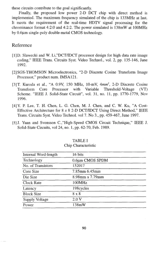
The 2-D DCT chip consists of mainly adders, memories and registers. Table I1 shows the simulated power dissipation of components. Thus, reducing the power consumption in these components will make more contribution to achieve low power.
A.
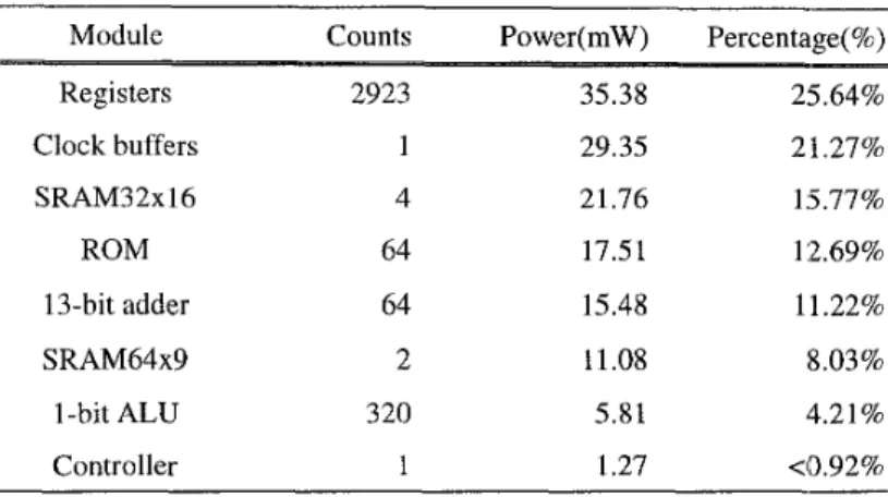
Adder DesignThe adder is used as the accumulator in calculating the 1-D DCT results. Since the adder operates at low voltage, the parallelism is employed in order to compensate for the speed loss. The adder adopts the square-root carry-select structure shown in Figure 2. After dividing the larger adder into several stages, these stages are implemented with Manchester adder for its improvement on the carry-lookahead by using a single gate for generating carry C j . Therefore, a large-
bit adder is formed by combining the square-root carry-select adder in architecture and the Manchester adder in stage circuit. Although the ripple-carry adder consumed less power than the Manchester adder, it is too slow to meet the speed requirement in our design. In addition, the Manchester adder gains more in circuit regularity as well as power saving than the carry-lookahead adder. B. Power-Saving
ROM
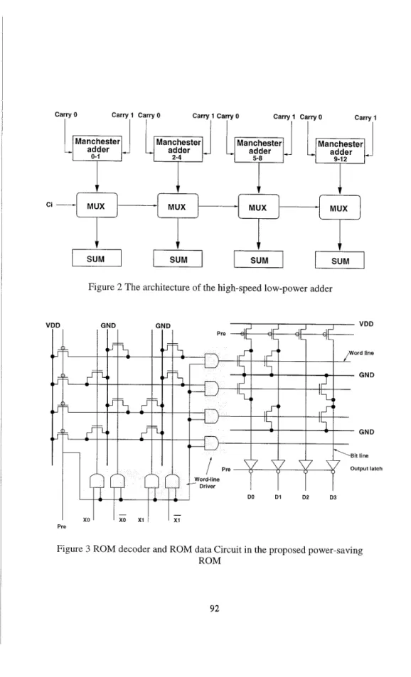
Since the 1-D .DCT in our chip is implemented by DA method, the ROM is needed to hold the content of the look-up table that is pre-computed. In order to eliminate the static power consumption due to the DC path existing in static pseudo-nMOS ROM, a better approach is to use pre-charged logic. The ROM decoder and data circuits are shown in Figure 3. An address transition detection (ATD) circuit is employed to generate the pre-charge signal pre, which is activated only when the input addresses change. During the pre-charge phase, pre
= 0 and the bit-lines are pre-charged to VDD. Meanwhile, the AND gates in decoder ensure that all pull-down paths through the NMOS are off during pre- charging. In the evaluation phase, pre = 1 and if the word-line is activated high, the bit-line is discharged. For the PMOS and NMOS don’t turn on simultaneously during pre-charging or evaluation phase, there is minimum DC path from V,,, to GND, and thus, minimum static DC power dissipation.can be obtained.
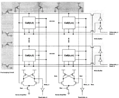
Since the proposed 2-D DCT is implemented with DA parallel architecture, the data reordering is needed for bit-serial word-parallel data operation. Thus, the two-port SRAM shown in Figure 4 is proposed for data mapping and data reordering. Note that the input port size n is different from the output port size m. The sense amplifier consists of across-coupled pair of PMOS transistors and NMOS input devices. This differential pair applies the positive ffeedback to accelerate the sense speed.
V. Chip Performance
By incorporating the module circuits discussed above, a low power 2-D DCT chip with direct method is proposed. Figure 5 shows a die photo of the 2-D DCT chip. It consists of about 152000 transistors and implemented in 0.6pm CMOS technology. The die size is about 70mm2 including pads. The maximum clock freqency is lOOMHz and typical power dissipation is around 138mW at 2V. The core characteristics are summarized in Table I. Besides, in order to understand more details about the power distribution in the designed chip, a power simulation at 100 MHz by components is shown in Table 11. From this table, it is obviously that registers consume most power than others do. Then, excluding the clock buffers, the first runner up is memory module. Hence, reducing the power consumption of registers and memories will contribute more to achieve the proposed chip. That is the reason why our low power design is emphasized on the components such as registers, memories and adders. The implementation in [ l ] and the product presented in [ 2 ] are not dedicated to low power design. Thus, they consume larger power. The chip reported by [3] which utilized variable threshold-voltage scheme by controlling back-bias voltage and better technology achieved a lOmW 2-D DCT core processor. However, the main consideration of this chip comes from the technology and circuit level. The main features of these chip implementations are summarized in Table 111. Our chip is design by taking the low power algorithm, architecture, and circuits into consideration. The ideas in both chips do not conflict. Hence, combining the low power algorithm and architecture in our chip and the variable threshold-voltage scheme in [3] will lead to a 2-D DCT chip with lower power dissipation than both two chips.
VI. Conclusion
A low-power high-performance 2-D DCT chip is proposed. The design features that contribute most to this result are as follows. First, the usage of the direct 2-D DCT algorithm reduces the 2-D DCT into 1-D DCT and some additions. Also, a fast algorithm of 1-D DCT is employed. Both of these decrease the computational complexity which means low power consumption per block operation. Besides, a parallel distributed arithmetic (DA) architecture with the direct 2-D DCT approach is proposed in order to compensate the speed loss due to the reduced internal supply voltage.
In addition to the considerations in algorithm and architecture level, low power design methdologies in logic-style and circuit level are applied to the real circuit implementation of the proposed 2-D DCT. Since adders, memories and registers are the main modules of the proposed DCT design, a pourer-saving in
these circuits contribute to the goal significantly.
Finally, the proposed low power 2-D DCT chip with direct method is implemented. The maximum frequency simulated of the chip is 133MHz at last. It meets the requirement of the real-time HDTV signal processing for the chrominance format 4:2:0 and 4:2:2. The power simulated is 138mW at lOOMHz by 0.6pm single-poly double-metal CMOS technology.
Reference
[ I ] D. Slawecki and W. Li,”DCT/IDCT processor design for high data rate image coding,” IEEE Trans. Circuits Syst. Video Technol., vol. 2, pp. 135-146, June 1992.
[2] SGS-THOMSON Microelectronics, “2-D Discrete Cosine Transform Image Processor,” product num. IMSA121.
[3]T. Kuroda et al., “A 0.9V, 150 MHz, 10-mV, 4mm2, 2-D Discrete Cosine Transform Core Processor with Variable Threshold-Voltage (VT) Scheme. ”IEEE J. Solid-state Circuit”, vol. 31, no. 11, pp. 1770-1779, Nov 1996.
[4]Y. P. Lee, T. H. Chen, L. G. Chen, M. J. Chen, and C. W. Ku, ”A Cost- Effective Architecture for 8 x 8 2-D DCTLDCT Using Direct Method,” IEEE Trans. Circuits Syst. Video Technol. vol7. No 3., pp. 459-467, June 1997. Solid-state Circuits, vol24, no. 1, pp. 62-70, Feb. 1989.
[5] J. Yuan and Svensson C.,”High-Speed CMOS Circuit Technique,” IEEE J.
TABLE I Chip Characteristic Internal Word-length 16 bits
Technology 0.6pm CMOS SPDM
No. of Transistors 152017
Core Size 7.85mm 6.45mm
Die Size 8.98mmx7.79mm
Clock Rate 1 OOMHz
Latency 198cycles
Block Size 8 x 8
Supply Voltage 2.0
v
TABLE I1
Simulated Power Dissipation by Components
Module Counts Power( mW) Percentage( %)
Registers 2923 35.38 25.64% 29.35 2 1.27% L II
-
Clock buffers 1 SRAM32x16 4 21.76 1:5.77% 1:2.69% 13-bit adder 64 15.48 11.22% SRAM64x9 2 11.08 8.03% 1 -bit ALU 320 5.81 84.21% Controller 1 1.27 4 9 2 % ROM 64 17.51 DSawecki et al.[l] SGS-THOMSON[2] T.Kuroda et a1.[3] TABLE I11 Processor Cornparsion 2pm 72.68mm2 67929 5V 5OMHz 5V 20MHz 0 . 3 ~ m 4mm2 120000 0.9V 15OMHz lOmWAuthors
I
Tech.I
CoreareaI
Trans.I
VoltageI
Clock rateOur Chip )0.6pmI 50.6mm2
I
152017I
2VI
lOOMHzI
138mWI
9
-
Figure 1 The proposed parallel DA 2-D DCT architecture
Carry1 Carry0 Carry 1 Carry 0 Carry 1
I /
I I
I
Carry 0I
Carry 1I
LTJ
adderFigure 2 The architecture of the high-speed low-power adder
Figure 3 ROM decoder and ROM data Circuit in the proposed power-saving ROM
Figure 4 The core of the two-port SRAM circuits include memory cells, write buffers, sence amplifiers and precharging circuits
Figure 5 Die Photo of the 2-D DCT Chip