Planar GaN p-i-n photodiodes with n
+-conductive channel formed by Si
implantation
M. C. Chen
Institute of Optical Science, National Central University, Jhongli 32001, Taiwan J. K. Sheua兲
Institute of Electro-Optical Science and Engineering, Advanced Optoelectronic Technology Center, National Cheng Kung University, Tainan 70101, Taiwan
M. L. Lee
Department of Electro-Optical Engineering, Southern Taiwan University of Technology, Tainan County 710, Taiwan
C. J. Kao and G. C. Chi
Department of Physics, National Central University, Jhongli 32001, Taiwan
共Received 24 January 2006; accepted 9 April 2006; published online 18 May 2006兲
In this study, planar GaN p-i-n photodiodes 共PDs兲 were fabricated by Si implantation into GaN-based p-i-n structure grown by metal organic vapor-phase epitaxy. Triple silicon implantation was performed to form a selective n+channel through the multilayer p-i-n structure. As a result of
n+-channel formation, a planar GaN p-i-n detector could be obtained. With the reverse bias below
2 V, the dark current density was well below 50 pA. The dark current increased significantly with an increase of reverse bias, which may be attributed to the incomplete damage共from implantation兲 removal and thereby result in the higher leakage current. The typical peak responsivity and the cutoff wavelength for the Si-implanted planar p-i-n PDs were around 0.13 A / W and 365 nm, respectively. In addition, the visible 共450 nm兲-to-UV 共365 nm兲 rejection ratio of around three to four orders could be extracted from the spectra response. Furthermore, the transient response measurements revealed that the full width at half maximum 共FWHM兲 of impulse response was as low as 1.12 ns. © 2006 American Institute of Physics. 关DOI:10.1063/1.2206687兴
Recently, III-V nitrides have become a focus of exten-sive research aimed for application in light emitters,1,2 high-temperature electronics3 and ultraviolet 共UV兲 photodiodes 共PDs兲.4
III-nitride based PDs are very promising candidates for practical application in the aforementioned areas due to their potentially high quantum efficiency, low noise, and sharp, tunable band edge.1,2 During the last several years, various types of GaN-based PDs have been proposed, among the suggested alternatives are p-i-n photodiodes and Schottky photodiodes with high responsivity.5 In theory, an ideal UV PD should be insensitive to visible and IR back-ground. Values of UV-to-visible rejection ratio, determining the photoresponse in UV region to photoresponse in visible region, should be maximized. When compared to Schottky barrier PDs, p-i-n PDs have a high breakdown voltage, a fast response speed, a sharp cutoff, and a high responsivity. The advantages above make p-i-n PDs attractive for practical ap-plication. However, we should note that most GaN-based devices are grown on top of insulating sapphire substrates. Thus, it is always necessary to etch away a part of the sample surface in order to fabricate a conventional GaN-based p-i-n PD. In other words, conventional GaN-based p-i-n PDs are nonplanar. Such a nonplanarity could result in at least minor drawbacks in PDs. For example, leakage current may increase depending on the perimeter of a device due to sur-face recombination resulting from etched sursur-face. Previously, we have reported the fabrication of GaN n+-p junction
di-odes formed by Si implantation into p-GaN. It has been dem-onstrated that it is possible to achieve a planar GaN p-i-n with reasonably good electrical properties. In this study, we demonstrate planar GaN p-i-n PDs fabricated by Si implan-tation into GaN-based p-i-n structure.
Prior to Si ion implantation, GaN-based p-i-n structures were grown by metal organic vapor-phase epitaxy on c-face sapphire substrates. The layer structure was comprised of a 300 Å thick GaN nucleation layer grown on the sapphire substrate and followed by a 3.5m thick Si-doped GaN layer 共nd⬃2⫻1018cm−3兲, a 0.15m thick undoped GaN absorption layer共n⬃3⫻1016cm−3兲, and a 500 Å thick Mg-doped GaN capping layer共na⬃5⫻1017cm−3兲. Details of the GaN growing procedures have already been described in other sources.6In this study, Triple silicon implantation was performed to form a selective n+ channel through the
multilayer p-i-n structure. Therefore, planar GaN p-i-n PD with a concentric-circle configuration could be obtained, as shown in the Fig. 1. The triple implantation condition共dose/ energy兲 was equal to 1.5⫻1014cm−2/ 40 KeV, 3
⫻1014cm−2/ 100 KeV, and 6⫻1014 cm−2/ 150 KeV. The
overall implantation depth was estimated to be about 0.25m.6 The implanted samples were then thermal an-nealed at 1100 ° C for 60 s. As a result, the p-GaN and the undoped GaN layers in the selective implanted area could be converted into a low-resisitivity n+-GaN channel connecting
the n+-GaN epitaxial layer. The electron concentration of the
implanted n+-GaN layer was around 3.2⫻1018cm−3, as
de-termined by Hall-effect measurement.7 p-type共Ni/Au兲 con-tacts and n-type共Ti/Al/Ti/Au兲 contacts were deposited and
a兲Author to whom correspondence should be addressed; electronic mail:
APPLIED PHYSICS LETTERS 88, 203508共2006兲
0003-6951/2006/88共20兲/203508/3/$23.00 88, 203508-1 © 2006 American Institute of Physics
patterned by e-beam evaporator and a standard liftoff pro-cess, respectively. Ti/ Al/ Ti/ Au 共30/120/80/150 nm兲 and Ni/ Au 共5/10 nm兲 metal contacts were then annealed in N2
ambient to serve as the contact materials on Si-implanted n+-GaN and p-GaN surfaces, respectively.
Room-temperature current-voltage共I-V兲 characteristics of these di-odes were then measured using an HP4146C semiconductor parameter analyzer. The spectral responsivity of the planar GaN p-i-n PD was also measured using an Xe arc lamp and a calibrated monochromator serving as the light source. The power of the monochromatic light was measured with a cali-brated silicon photodiode and then illuminated onto the front side of the PDs. During transient time measurement, a pulse N2 laser emitting at 337 nm was used as the excitation
source. The pulse width of the laser was 500 ps. A 1 GHz oscilloscope was used to measure the photocurrent generated by the GaN PDs under pulse N2laser illumination.
Figure 2 shows typical I-V characteristics of the planar GaN p-i-n PDs. We can see that when the reverse bias was below 2 V, the dark current density was well below 50 pA. However, the dark current density was larger than that of GaN-based p-i-n PDs grown on laterally epitaxially over-grown GaN.3In this study, the leakage current of nonplanar devices made from the same structure was also measured for comparison. For a given reverse bias of 2 V, the typical leak-age current was around 10 pA. In Fig 2, the bias-dependent reverse I-V characteristics may be explained by the presence of trap levels within the band gap, thereby resulting in trap-assisted tunneling current. The trap levels are most likely associated either with structural defects or with point defects,
including process damage. It is a known fact that defects in GaN共i.e., dislocation originating from large lattice mismatch between sapphire and GaN兲 can reveal themselves in high leakage currents.3 In this case, the implanted damage would also play an important role in the origins of trap levels and hence appearance of leakage current. It is worth to note that further analysis, such as temperature-dependent electrical characterization, is needed to clarify the charged state of trap and extract the trap density. A detailed study on the implan-tation induced trap levels are underway and will be reported in other research work. On the other hand, one can see that the reverse current increases significantly under influence of reverse bias especially when the reverse bias voltages exceed 2 V, as shown in Fig. 2. This phenomenon may be attributed to the fact that the p-type layer was completely depleted when the reverse bias voltages were above 2 V, because the thickness of the p layer was only 50 nm and its hole concen-tration was around 3⫻1017cm−3. Therefore, one can widen
the thickness and/or increase the hole concentration of the p layer to alleviate the above-mentioned bias-dependent re-verse current. However, the approach described above would result in the reduction of responsivity due to the absorption of the thick p layer. For p type doping of GaN, deep acceptor level occurs due to larger hole mass and creates difficulties for p-type doping and the very low activation efficiency of dopants at room temperature for GaN.8Previous reports have shown that one can increase acceptor ionization efficiency and hole concentration by introducing Mg-doped AlGaN / GaN strained layer superlattice共SLS兲 structure into p-GaN.8 Additionally, the enhanced responsivity of GaN-based p-i-n UV PDs with low-resistivity SLS have been demonstrated.9
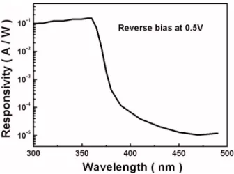
Figure 3 shows the typical spectral responsivity of the Si-implanted planar GaN p-i-n PDs under reverse bias. It was found that the cutoff occurred at around 365 nm. Theo-retically, when the incident photon energy is greater than the GaN band-gap energy, all optical energy is absorbed, and in turn transferred to photocurrent. For this reason, if GaN p-i-n PDs are to have a broad spectral responsivity, the high energy photons absorbed by the p-GaN layer should be mini-mized. The Si-implanted planar GaN p-i-n PDs showed a flat short-wavelength spectral response due to the thickness of the p-GaN top layer being only 50 nm. In other words, only photons with energy close to or less than the band-gap en-ergy of GaN could reach deeper to produce electron-hole
FIG. 1. Schematic device structure in cross-section view.
FIG. 2. Typical I-V characteristics of the planar GaN p-i-n PDs taken under dark and UV illumination.
FIG. 3. Typical spectral responsivity of the planar GaN p-i-n PDs with a reverse bias of 0.5 V.
203508-2 Chen et al. Appl. Phys. Lett. 88, 203508共2006兲
pairs in the depletion region共i layer兲 if p-i-n PDs were de-signed to have thick p-GaN top layer. To obtain the trans-mission rate of Ni/ Au top contact used in the present de-vices, the optical transmission of 550 ° C-annealed Ni/ Au 共5/10 nm兲 thin film deposited on polished sapphire was measured. If T + R + A = 1, the sum of the reflection rate共R兲 and absorption rate共A兲 of the Ni/Au top contact was around 48%, at 365 nm, since the transmission rate共T兲 of the Ni/Au film was around 52%. In addition, the Fresnel reflection rate was also estimated to be around 17%. Typically, the peak responsivity of the planar Si-implanted GaN p-i-n PDs was estimated to be around 0.13 A / W, corresponding to a peak quantum efficiency of around 45%. The visible 共450 nm兲-to-UV 共360 nm兲 rejection ratio of around 10 000 could be extracted from the spectra response, as shown in Fig. 3. These values are very close to that of nonplanar de-vices which have a rejection ratio of around 9000–10 000 extracted from the same wavelength range. In addition, the nonplanar devices exhibited a typical responsivity 共at 360 nm兲 of around 0.15 A/W.
Figure 4 shows a typical transient response of a GaN planar p-i-n PD excited by pulse N2 laser. In this study, it
was found that the measured fall times were all around 1.12 ns. It was also found that the fall times were indepen-dent from the applied reverse bias. In theory, transient re-sponse will become faster with the increase of reverse bias, since the extended depletion region will reduce the junction capacitance if the fall time of impulse response is dominated
by RC time constant. In addition, the increased bias will also result in an increased electrical field in the absorption layer and hence reduce the drift time of carrier. Bias-independent transient response may be attributed to the fact that the fall time of our Si-implanted planar GaN p-i-n PD is entirely limited by RC time constant of the detection circuit.
Summarizing our research we should note that GaN p-i-n PDs featuring a planar structure were fabricated by implanting Si atoms into GaN-based p-i-n structure. The dark current density was well below 50 pA, when the reverse bias was below 2 V. In addition, the dark current increased drastically with increase of reverse bias, which may be due to incomplete damage共from implantation兲 removal resulting in the higher leakage current. The Si-implanted planar p-i -n PDs exhibited a peak responsivity of around 0.13 A / W. In addition, the visible 共450 nm兲-to-UV 共365 nm兲 rejection ratio of around 10000 could be extracted from the spectra response. For the transient response measurements, the typi-cal full width at half maximum 共FWHM兲 of impulse re-sponse was as low as 1.12 ns.
The authors of the research would like to acknowledge the Center for Micro/Nano Technology Research, National Cheng Kung University, Tainan, Taiwan, for providing equipment and technical and financial support. We also ex-tend gratitude to the great support offered by National Sci-ence Council and Ministry of Economic Affairs and provi-sion of research grants NSC 93-2112-M-008-034, NSC 94-2215-E-006-015, and MOEA-94-EC-17-A-07-S1-043.
1J. I. Pankove, Mater. Res. Soc. Symp. Proc. 162, 515共1990兲.
2E. Monroy, E. Muñoz, F. J. Sánchez, F. Calle, E. Calleja, B. Beaumout, P.
Gibart, J. A. Muñoz, and F. Cussó, Semicond. Sci. Technol. 13, 1042 共1998兲.
3G. Parish, S. Keller, P. Kozodoy, J. A. Ibbetson, H. Marchand, P. T. Fini,
S. B. Fleischer, S. P. DenBaars, and U. K. Mishra, Appl. Phys. Lett. 75, 247共1999兲.
4E. Monroy, M. Hamilton, D. Walker, P. Kung, F. J. Sánchez, and M.
Razeghi, Appl. Phys. Lett. 74, 1171共1999兲, and references therein.
5A. Osinsky, S. Gangopadhyay, J. W. Yang, R. Gaska, D. Kuksenkov, H.
Temkin, I. K. Shmagin, Y. C. Chang, J. F. Muth, and R. M. Kolbas, Appl. Phys. Lett. 72, 551共1998兲, and references therein.
6J. K. Sheu, M. L. Lee, C. J. Tun, C. J. Kao, L. S. Yeh, M. J. Chen, and G.
C. Chi, Appl. Phys. Lett. 81, 4263共2002兲, and references therein.
7J. K. Sheu, M. L. Lee, C. J. Tun, C. J. Kao, L. S. Yeh, C. C. Lee, S. J.
Chang, and G. C. Chi, IEEE J. Sel. Top. Quantum Electron. 8, 767共2002兲.
8J. K. Sheu and G. C. Chi, J. Phys.: Condens. Matter 14, R657共2002兲. 9L. S. Yeh, M. L. Lee, J. K. Sheu, M. G. Chen, C. J. Kao, G. C. Chi, S. J.
Chang, and Y. K. Su, Solid-State Electron. 47, 873共2002兲. FIG. 4. Typical impulse response of the planar GaN p-i-n PDs with a
reverse bias of 3 V.
203508-3 Chen et al. Appl. Phys. Lett. 88, 203508共2006兲