Low-temperature and catalyst-free synthesis of well-aligned ZnO
nanorods on Si (100)
Sai-Chang Liu and Jih-Jen Wu*
Department of Chemical Engineering, National Cheng Kung University, Tainan 701, Taiwan. E-mail: [email protected]
Received 22nd April 2002, Accepted 24th June 2002
First published as an Advance Article on the web 9th August 2002
Well-aligned ZnO nanorods have been grown on Si (100) substrates using a simple, catalyst-free CVD method at low temperatures. Structural analyses show that the nanorods grown on Si (100) are preferentially oriented in the c-axis direction. An amorphous SiOxlayer in the interface of ZnO nanorods and Si (100) is observed
from the HRTEM and EELS images. The well-aligned ZnO nanorods exhibit a strong PL emission of 380 nm at room temperature. A negligible green band emission in the PL spectra indicates that there is a very low concentration of oxygen vacancies in the highly oriented ZnO nanorods. Diameter control of the well-aligned and high-quality ZnO nanorods on Si (100) substrates is achievable by varying the growth conditions.
1 Introduction
Since carbon nanotubes were discovered,1 syntheses of one dimensional (1-D) nanoscale materials of various elements and compounds have stimulated much interest worldwide because of their potential uses in both fundamental studies and applications.2Zinc oxide, which has already been widely used in transparent conducting films, varistors, solar cell windows, and bulk acoustic wave devices,3–5 is a II–VI
compound semiconductor with a wide direction bandgap of 3.37 eV and a large exciton binding energy of 60 meV at room temperature. The strong exciton binding energy which is much larger than the thermal energy at room temperature (ca. 25 meV) can ensure an efficient exciton emission at room temperature.6 Therefore, ZnO is recognized as a promising
photonic material in the blue-UV region. Room-temperature UV lasing properties have been demonstrated from ZnO epitaxial films,6microcrystalline thin films,7nanoclusters8and nanowires.9 The growth of 1-D ZnO nanostructures has attracted considerable attention recently due to their promising application in optoelectronic nanodevices. One-dimensional single-crystalline ZnO nanostructures synthesized by various high-temperature processes, such as vapor–liquid–solid (VLS) methods (¢900uC)10,11
and thermal evaporation (1400uC)12
have been reported.
Recently, we have demonstrated a simple, catalyst-free CVD approach for the growth of single-crystalline ZnO nanorods on fused silica substrates at a low temperature of around 500uC.13
In present work, growth and characterization of the highly oriented ZnO nanorods on Si (100) are further studied in detail. Systematic study of ZnO nanorod growth and microstructural analyses of the ZnO nanorods on Si (100) are demonstrated in this paper. We believe the approach presented here is a simple one for practical application of ZnO nanostructures to optoelectronic devices.
2 Experimental
ZnO nanorods were grown in a 3@ quartz tube insert to a two-temperature-zone furnace. A schematic of the two-tempera-ture-zone furnace is shown in Fig. 1. The quartz tube was well-sealed for being able to maintain a base pressure of 5.0 6 1023Torr. Zinc acetylacetonate hydrate [Zn(C5H7O2)2?xH2O,
Lancaster, 98%], which was employed as the zinc source, placed on a cleaned Pyrex glass container, was loaded into the
low-temperature zone of the furnace. The temperature was controlled to be at 130–140uC to vaporize the solid reactant. The vapor was carried by a N2/O2 flow into the higher
temperature zone of the furnace in which Si (100) substrates were located. Si (100) substrates were cleaned in an ultrasonic bath of acetone for 20 min and were then dipped in HF solution and deionized water before being loaded into the quartz tube. It should be noted here that there is no catalytic metal pre-treated on the Si (100) substrates. In this study, the total pressure of the quartz tube and the deposition time of ZnO nanorods were 200 Torr and 6 h, respectively.
The morphology and size distribution analyses of the nanorods were examined using scanning electron microscopy (SEM, Hitachi, S-4200). A high-resolution (HR) SEM (JEOL, JSM-6700 F) was also employed to study the detailed mor-phology of the ZnO nanorods. The crystal structure of the nanorods was analyzed using X-ray diffraction (XRD, Rigaku D/MAX-2000) and transmission electron microscopy (TEM, JEOL, JEM-4000EX). Electron energy-loss spectroscopy (EELS, GIF 2000) equipped on a TEM (Philips Tecnai 20) was employed to analyze the qualitative compositions of the products. Photoluminescence (PL) studies were conducted using a Hitachi F-4500 fluorescence spectrophotometer with a Xe lamp at room temperature. The excitation wavelengths were 325 nm.
3 Results and discussion
3.1 Systematic study of ZnO nanorod growth
(1) Effect of substrate temperature. For study of the effect of the substrate temperature on the formation of well-aligned ZnO nanorods, syntheses of ZnO nanorods on Si (100) were performed at 450, 500, and 550uC under the following constant conditions: source vaporizing temperature ~ 135 uC, N2/O2
flow rate ~ 250/250 sccm (standard cubic centimeters per
Fig. 1 Schematic diagram of the two-temperature-zone furnace.
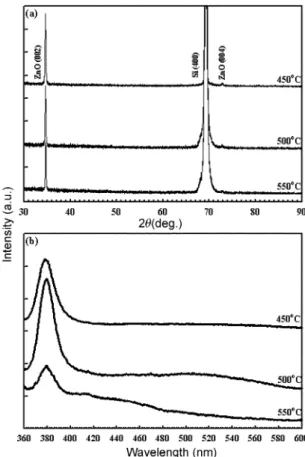
minute), and total pressure ~ 200 Torr. The SEM image shown in Fig. 2(a) reveals that the average diameter and length of the ZnO nanorods synthesized at 450 uC are 45 nm and 200 nm, respectively. As shown in Fig. 2(a)–(c), the diameters of the ZnO nanorods increase as the substrate temperature is increased. Fig. 2(c) shows that the characteristic of high density of well-aligned nanorods is not apparent at a 550uC. Therefore, it does not favor the formation of well-aligned ZnO nanorods at growth temperatures higher than 500uC.
The crystal structure of the nanorods grown at various substrate temperatures was examined by XRD. As shown in Fig. 3(a), in addition to the diffraction peak of Si (400), which is ascribed to the substrate, the diffraction peaks of ZnO (002) and (004) appear in the XRD spectra of the nanorods grown at 450 and 500uC, indicating that the ZnO nanorods grown on substrates are preferentially oriented in the c-axis direction. The sample with poorly-aligned nanorod mor-phology, grown at 550 uC, also shows the characteristic of preferential orientation in the c-axis direction as shown in Fig. 3(a).
The room temperature PL spectra of nanorods grown at various temperatures are shown in Fig. 3(b). The UV emission of 380 nm, which is the contribution of the near band edge emission of the wide band gap ZnO, is observed in the three spectra of ZnO nanorods grown at various substrate tempera-tures. In addition to the UV emission an almost negligible green band (480–580 nm) also appears in the PL spectrum of ZnO nanorods grown at 500uC. It has been suggested that the green band emission corresponds to the singly ionized oxygen
vacancy in ZnO.14The almost negligible or even absent green band in these PL spectra indicates a very low concentra-tion oxygen vacancy in the ZnO nanorods grown by zinc acetylacetonate. The PL spectrum of the ZnO nanorods grown at 550uC also shows the appearance of a blue band emission (400–480 nm). The blue band emission of ZnO films has been also reported using cathodoluminescence.15However, the mechanism of this emission is not yet clear.
(2) Effect of zinc source vaporizing temperature. Zinc acetylacetonate within a Pyrex glass container loaded into the low-temperature zone of the furnace was controlled to be at three temperatures, of 130, 135 and 138uC, for study of the growth behavior of the well-aligned ZnO nanorods. The substrate temperature and the N2/O2 flow rate are kept at
500uC and 250/250 sccm, respectively. High densities of well-aligned ZnO nanorods were formed on the Si substrates at the three Zn source vaporizing temperatures, as shown in Fig. 4(a)–(c). The lengths of the ZnO nanorods are almost the same but the diameters are reduced from 70 to 55 nm when the vaporizing temperature is increased from 130 to 138uC for a 6 h deposition period. The PL spectra of the well-aligned ZnO nanorods grown under various vaporizing temperatures of zinc acetylacetonate are illustrated in Fig. 4(d). It reveals a strong UV emission and a negligible or absent green emission observed in the three spectra, indicating the good quality of these ZnO nanorods.
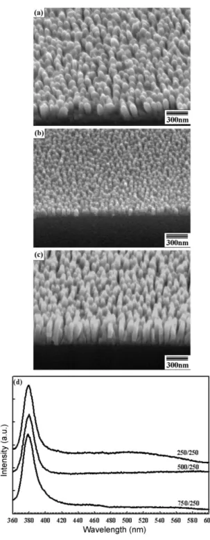
(3) Effect of N2/O2flow rate. For study the effect of N2/O2
flow rate, the growth of ZnO nanorods was performed under various N2/O2 flow rates, including 250/250, 500/250 and
750/250 sccm at a substrate temperature of 500 uC and a zinc acetylacetonate vaporizing temperature of 135uC. High densities of well-aligned ZnO nanorods were also formed on the Si substrates at various N2/O2 flow rates, as shown in
Fig. 2 SEM images of the ZnO nanorods grown on Si (100) at various substrate temperatures: (a) 450uC, (b) 500 uC, and (c) 550 uC, using a source vaporizing temperature of 135uC and a N2/O2flow rate of 250/
250 sccm.
Fig. 3 XRD (a) and PL (b) spectra of the ZnO nanorods shown in Fig. 2(a)–(c).
Fig. 5(a)–(c). For the same deposition time of 6 h, ZnO nanorods synthesized at a N2/O2 flow rate of 750/250 sccm
possess the longest average length of 280 nm while those grown at 500/250 sccm exhibit the shortest average length of 100 nm and the smallest average diameter of 45 nm among the three N2/O2 flow rates. PL spectra of these ZnO nanorods, as
shown in Fig. 5(d), indicate that good quality, well-aligned ZnO nanorods can be synthesized in a rather wide range of N2/O2flow rate.
(4) Diameter-controlled growth of the well-aligned ZnO nanorods. Diameter-controlled growth of well-aligned ZnO nanorods has been achieved using the catalyst-free CVD approach. Average diameters ranging from 70 to 45 nm for
well-aligned ZnO nanorods of good quality can be synthesized on Si (100) by adjusting the growth conditions such as substrate temperature, vaporizing temperature and N2/O2flow rate as
mentioned above.
3.2 Microstructural characterization of the well-aligned ZnO nanorods on Si (100)
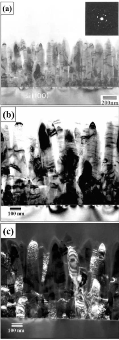
In order to learn how the well-aligned ZnO nanorods were grown on the Si (100) substrate, TEM was employed to investigate the microstructure of the ZnO nanorods. The cross-sectional TEM image and corresponding electron diffraction pattern of the ZnO nanorods grown on Si (100) are shown in Fig. 6(a). It reveals that most of the nanorods were grown in a direction perpendicular to the Si (100) substrate. While the
Fig. 4 SEM images of the ZnO nanorods grown on Si (100) at various zinc source vaporizing temperatures: (a) 130uC, (b) 135 uC, and (c) 138uC, at a substrate temperature of 500 uC and a N2/O2flow rate of
250/250 sccm; (d) PL spectra of the ZnO nanorods shown in (a)–(c).
Fig. 5 SEM images of the ZnO nanorods grown on Si (100) using various N2/O2flow rates: (a) 250/250 sccm, (b) 500/250 sccm and (c)
750/250 sccm, at a substrate temperature of 500 uC and a source vaporizing temperature of 135uC; (d) PL spectra of the ZnO nanorods shown in (a)–(c).
selective diffraction pattern (SAD) of the cross-sectional image shows a discrete ring pattern, indicating that the ZnO nanorods grow on Si (100) randomly in the a-axis direction although they are preferentially oriented in the c-axis direction. Typical bright- and dark-field cross-sectional images of the ZnO nanorods on Si (100) are illustrated in Fig. 6(b) and (c), respectively. The dark-field image indicates that the nanorod possesses the single crystalline structure.
High-resolution (HR) TEM was employed to study the interfacial region of the ZnO nanorod and the Si (100) sub-strate. The HRTEM image, as shown in Fig. 7, reveals that the spacing of 0.26 nm between adjacent lattice planes corresponds to the d-spacing of ZnO (002) crystal planes, and that the ZnO (002) planes are parallel to the Si (100) planes, confirming the XRD analyses of ZnO nanorods being preferentially oriented in the c-axis direction. Furthermore, a 3-nm-thick amorphous layer between the ZnO nanorod and Si substrate is observed in Fig. 7. Elemental analyses of the amorphous interfacial layer were further undertaken using EELS. EELS mapping images of Si, O and Zn elements, as well as the corresponding HRTEM image, are shown in Fig. 8. In contrast to the Si and O mapping images, there is no transition layer appearing in the Zn mapping image, indicating that the amorphous interfacial layer is composed of Si and O elements. Therefore, a thin SiOx
amorphous layer was formed on the Si (100) substrate first at a growth temperature of 500uC, and then ZnO nanorods were grown on the SiOxpreferentially oriented in the c-axis
direction.
3.3 Mechanism of ZnO nanorod growth
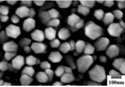
The growth of 1-D nanostructures has been demonstrated by various methods.2,16,17Apart from the template-based growth method,16 the VLS mechanism has been the most popular method for the growth of 1-D nanomaterials.2 In the VLS mechanism, metallic particles as catalyst are usually observed at the ends of the 1-D nanostructures after growth.2,10,11In the present work, there are no additional metal particles appearing on the top or the bottom of the nanorods, implying a non-VLS approach for the formation of the ZnO nanorods. The screw dislocation mechanism has also been reported to be a mechanism for the formation of the nanorods.17A conic tip with spiral morphology at the end of the nanorods, resulting from the existence of a screw dislocation whose line is parallel to the axis of the nanorods, is the evidence for nanorod growth via the screw dislocation mechanism. Fig. 9 shows a high-resolution SEM image of the tops of the ZnO nanorods. A well-faced prismatic morphology instead of the spiral morphology is observed on the tops of the ZnO nanorods, indicating that the
Fig. 6 TEM cross-sectional image of ZnO nanorods grown on the Si (100) substrate: (a) low magnification image shows nanorods grown with a direction perpendicular to the substrate; the corresponding SAD pattern is shown in the inset. (b) and (c) Typical bright- and dark-field images of the ZnO nanorods, respectively.
Fig. 7 High-resolution TEM image of a single crystalline ZnO nanorod grown on Si (100).
Fig. 8 EELS mapping images of the interfacial region of the ZnO nanorod and Si (100): (a), (b) and (c) are Si, O and Zn elemental mapping images, respectively; (d) the corresponding HRTEM image of the EELS mapping images.
growth of the ZnO nanorods did not follow the screw dislocation mechanism in this study. It has been demonstrated that the morphology of the crystals is related to the relative growth rates of various crystal faces bounding the crystal; these rates are not only determined by the internal structure of the crystal but are also affected by the growth conditions.18SEM
images indicate that the relationship of the growth rates (R) of the directions of the ZnO crystal faces is Rv001wwRv101ww Rv100w, resulting in the formation of the ZnO nanorods
preferentially oriented in the c-axis direction with prismatic morphology on the tops. The relative growth rate of these crystal faces of the ZnO nanorods was affected by growth conditions. Therefore, various aspect-ratios of the well-aligned ZnO nanorods were successfully grown on the substrates in the present work.
4 Conclusion
Using zinc acetylacetonate and O2reactants, well-aligned and
good-quality ZnO nanorods can be synthesized at temperatures lower than 500 uC as well as a rather wide range of zinc source vaporizing temperatures and N2/O2flow rates. Diameter
control of the well-aligned and high-quality ZnO nanorods on the Si (100) substrates is achievable by varying the growth conditions. The highly oriented ZnO nanorods exhibit a strong PL emission of 380 nm at room temperature and green band emission is negligible in the PL spectra of the well-aligned ZnO nanorods. Structural analyses show that the nanorods grown on Si (100) are preferentially oriented in the c-axis direction. An
amorphous SiOxlayer at the interface of the ZnO nanorods
and Si (100) substrate is observed from the HRTEM and EELS images. We believe the approach presented is a simple one for practical application of ZnO nanostructures to optoelectronic devices.
Acknowledgements
The authors would like to thank Professor Y. Chen, Dr L. C. Chen and Dr X. J. Guo for help on PL, HRSEM and TEM measurements, respectively. The financial support of this work, by the National Science Council in Taiwan under Contract No. NSC 89-2214-E-006-023, is gratefully acknowledged.
References
1 S. Iijima, Nature, 1991, 354, 56.
2 C. M. Lieber, Solid State Commun., 1998, 107, 607.
3 P. Verardi, N. Nastase, C. Gherasim, C. Ghica, M. Dinescu, R. Dinu and C. Flueraru, J. Cryst. Growth, 1999, 197, 523. 4 J. F. Cordaro, Y. Shim and J. E. May, J. Appl. Phys., 1986, 60,
4186.
5 T. L. Yang, D. H. Zhang, J. Ma, H. L. Ma and Y. Chen, Thin Solid Films, 1998, 326, 60.
6 D. M. Bagnall, Y. F. Chen, Z. Zhu, T. Yao, S. Koyama, M. Y. Shen and T. Goto, Appl. Phys. Lett., 1997, 70, 2230. 7 P. Zu, Z. K. Tang, G. K. L. Wang, M. Kawasaki, A. Ohtomo,
H. Koinuma and Y. Segawa, Solid State Commun., 1997, 103, 459. 8 H. Co, J. Y. Xu, E. W. Seelig and R. P. H. Chang, Appl. Phys.
Lett., 2000, 76, 2997.
9 M. H. Huang, S. Mao, H. N. Feick, H. Yan, H. Kind, Y. Y. Wu, E. Weber and P. D. Yang, Science, 2001, 292, 1897.
10 Y. C. Kong, D. P. Yu, B. Zhang, W. Fang and S. Q. Feng, Appl. Phys. Lett., 2001, 78, 407.
11 M. H. Huang, Y. Wu, H. Feick, N. Tran, E. Weber and P. Yang, Adv. Mater., 2001, 13, 113.
12 Z. W. Pan, Z. R. Dai and Z. L. Wang, Science, 2001, 291, 1947. 13 J.-J. Wu and S.-C. Liu, Adv. Mater., 2002, 14, 215.
14 K. Vanheusden, W. L. Warren, C. H. Seager, D. R. Tallant, J. A. Voigt and B. E. Gnade, J. Appl. Phys., 1996, 79, 7983. 15 Z. Fu, B. Lin, G. Liao and Z. Wu, J. Cryst. Growth, 1998, 193, 316. 16 W. Han, S. Fan, Q. Li and Y. Hu, Science, 1997, 277, 1287. 17 X. S. Peng, G. W. Meng, J. Zhzng, X. F. Wang, Y. W. Wang,
C. Z. Wang and L. D. Zhang, J. Mater. Chem., 2002, 12, 1602. 18 W.-J. Li, E.-W. Shi, W.-Z. Zhong and Z.-W. Yin, J. Cryst. Growth,
1999, 203, 186. Fig. 9 High-resolution SEM image of the ZnO nanorods grown on
Si (100).