Research Express@NCKU Volume 22 Issue 9 - November 30, 2012 [ http://research.ncku.edu.tw/re/commentary/e/20121130/1.html ]
Energy Harvesting from the Obliquely Aligned InN
Nanowire Array with a Surface Electron-Accumulation
Layer
Nai-Jen Ku1, Chao-Hung Wang1, Jun-Han Huang1, Hsin-Chiao Fang1, Po-Chien Huang1, Chuan-Pu Liu2,*
1Department of Materials Science and Engineering, National Cheng Kung University, Tainan, 701 (Taiwan)
2Department of Materials Science and Engineering; Center for Micro/Nano Science and Technology;
Research Center for Energy Technology and Strategy; Advanced Optoelectronic Technology Center, National Cheng Kung University, Tainan, 701 (Taiwan)
Adv. Mater., DOI: 10.1002/adma.201203416
P
iezoelectric materials such as ZnO and III-nitride are gaining increasing attention for their energy-related applications, including high-brightness light-emitting diodes (LEDs), full-spectrum solar cells, and nanogenerators. Because of the inconvenience of using chemical batteries to power wireless sensors, harvesting energy from ambient mechanical movements in variable and uncontrollable environments is an effective method of poweringwireless mobile electronics for a wide range of applications in everyday life. The operating principle of a nanowire-based nanogenerator involves the unique coupling of the piezoelectric and semiconducting properties and the gating effect of the Schottky barrier formed between metal tips and semiconductor nanomaterials.
Consequently, nanogenerators convert mechanical energy from ambient movement into electricity that can be used to power nanodevices without batteries. Researchers have made great progress in developing piezoelectric nanogenerators based on II-VI compound semiconductor nanomaterials such as ZnO,1,2 ZnS,3 and CdS,4 which have great potential for the integration of piezotronics and nanogenerators. Recent efforts to enhance nanogenerator efficiency have focused on materials with higher piezoelectric coefficients, including poly(vinylidene fluoride) (PVDF) nanofibers,5 BaTiO3 thin films,6 and lead zirconate titanate (PZT) nanofibers.7 Group-III nitride materials, which are noted for their tunable, direct bandgap and good chemical stability, are also characterized by pronounced piezoelectric properties because of their wurtzite crystal structure.8 The calculated piezoelectric potentials increasing in the sequence of AlN, GaN, and InN lead to increasing levels of electricity generation, as observed in experiments.8 Among all the III-nitrides, InN possesses the smallest Young's modulus and the best conductivity for voltage output. Because of its unique piezoelectric properties, a single InN nanowire (NW) can generate an output voltage of up to 1 V, which is the highest voltage reported for this type of wire.9 Unlike ZnO, InN possesses a two-dimensional electron gas (2DEG) at the grown surface.
This surface electron-accumulation layer is accompanied by a large downward band bending relative to the Fermi level, which is pinned well above the conduction-band maximum at the surface,10–12 whether InN is clean13 or oxidized.14 The microscopic origin of surface band bending in InN has been attributed to donor-type surface states associated with In-In bonding (In adlayers).15 The presence of the occupied In–In bond states above the conduction band minimum may account for the observed electron accumulation on InN polar surfaces.
In addition to the commonly investigated In- and N-polar c-plane surfaces, surface electron accumulation has been observed on the nonpolar a-plane13 and m-plane,16 and even the zinc-blende (001) surface.13
The current design of DC nanogenerators demands both compressive and tensile strain simultaneously created inside the NW to create a piezopotential voltage drop across the NW diameter. The induced voltages are measured using a conductive tip of an atomic force microscope (AFM) or a pyramid-shaped electrode to bend the piezoelectric nanomaterial. However, this method is inherently limited by the degree of freedom in operation because the tip slides off the nanowire at a certain angle of deflection. The proposed method uses glancing- angle deposition to deliberately control nanorods in the desired orientation after growth to maximize the deformation and achieve the highest output power using molecular beam epitaxy (MBE).
Recent studies on nanogenerators have focused on the design of new functional materials with controllable size, shape, and structures. For a vertically aligned NR array, the maximal generated potential is directly related to the maximal deflection of nanostructures and the aspect ratio of NRs.8 Therefore, obliquely aligned large-area InN nanostructures with various aspect ratios are used to maximize the deformation for the highest output power.
Two types of one-dimensional obliquely aligned InN nanostructures were fabricated, denoted as InN nanorods (NRs) and nanowires (NWs), as shown in Figure 1a,b and Figure 1c,d, respectively. Whereas typical InN NRs are characterized by a diameter of approximately 114 ± 16.5 nm and a density of 1.0 × 1010 cm−2, the NWs exhibit a much smaller diameter of approximately 43 ± 19.2 nm and a density of 3.7 × 109 cm−2. Both NRs and NWs are obliquely aligned to the substrate with a height of approximately 1 μm and exhibit a high degree of uniformity in size and height. Figure 1e shows a cross-sectional transmission electron microscopy (TEM) image of InN NRs grown on ZnO nanopillars. Figure 1f shows a high-resolution (HR) TEM cross-sectional image of a single oblique InN NR along the direction, showing the inclined sidewall subtending an angle of approximately 43° to the top, flat c-plane corresponding to the semipolar r-plane. Therefore, a typical InN NR consists of a top (0002) plane and six r-plane sidewalls. The coupled plasmon-LO-phonon mode10,17 at approximately 435 cm−1 in the μ-Raman spectrum (see Figure 1S in the Supporting Information for details) confirms the presence of the quantized surface electron-accumulation layer. This implies that the electron concentration is on the order of 1019–1020 cm−3 for the entire exposed surface region.
Figure 1. Tilted-view scanning electron microscopy images of: a, b) the thicker InN nanorod sample, and c, d) the thinner InN nanowire sample. e) Cross-sectional TEM image of an obliquely aligned InN nanorod array grown on ZnO nanopillars. f) High-resolution TEM image of an InN nanorod near the top surface.
To explore plane and force-dependent piezotronic properties, localized I–V curves of the c-plane and r- plane surface of a singe oblique InN NR were obtained using a stationary conductive-AFM (C- AFM) tip. The measurement layout and equivalent circuit of the tip-to-InN Schottky diode are shown in Figure 2Sa,b in the Supporting Information and it can be considered as a back-to-back Schottky diode.
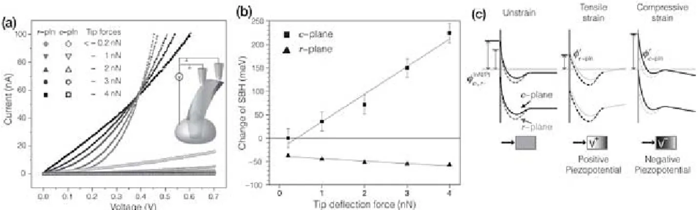
Figure 2a shows two sets of I–V characteristics taken from the c- and r-planes under various tip-deflection forces (ranging from 0 to 4 nN) exerted by a Pt tip.
The inset shows the experimental setup. When a positive bias voltage (V > 0) is applied to an InN NR through the Ag-electrode side with a grounded Pt tip, the voltage drop occurs mainly at the reverse-biased Schottky barrier Φs at the InN-to-tip interfaces. This reversely biased Schottky barrier dominates the I–V characteristics in this case. For any given voltage and tip-deflection force, the current is lower for the c- plane than the r-plane, indicating that a higher Schottky barrier height (SBH) is involved with the c- plane.18 Assuming that electron tunneling makes little contribution in the large-bias region,18 the dominant electron conduction through the SB for the c- and r- planes is a thermionic emission and diffusion (TED) mechanism,19–21 as confirmed by the perfect fit to the logarithmic curve of current with V1/4 shown in Figure 3S in the Supporting Information. At a given voltage in Figure 2a, increasing the tip-deflection force suppresses the current from the c-plane. Conversely, increasing the tip force increases the current from the r-plane when the bias is lower than 0.4 V but decreases the current when the bias exceeds 0.4 V.
Figure 2. a) Crystal-face and tip-deflection force-dependent I–V characteristics of an InN nanorod measured at the c-plane and r-plane by C-AFM. b) Derived piezopotential-induced SBH change relative to the unstained c- plane as a function of tip-deflection force based on the TED model. c) Schematic energy-band diagram of the Schottky contact at the c-plane and r-plane under the influence of strain-induced piezopotential.
Figure 2b shows the calculated piezopotential-induced SBH change at any state relative to the unstrained c- plane as a function of the tip-deflection force from the TED equation.19 The SBH increases by 224.0 meV as the tip force increases from 0 to 4 nN for the c-plane, but decreases slightly by 19.2 meV for the r-plane. The SBH for the semipolar r-plane is always lower than that of the c-plane, and the difference increases with the tip force from 37.6 meV at 0 nN to 281.0 meV at 4 nF. The I–V characteristics from the r-plane gradually evolve from rectifying behavior to ohmic characteristics as the tip force increases. Conversely, the rectifying ratio of the I–V curves for the c-plane increases as the tip force increases. The current change with the tip force results from the combined effects of the piezopotential-induced SBH change under the influence of the surface electron- accumulation layer, and the piezopotential gating effect reduces the NR conductance. The piezopotential repels electrons to the stretched side of the surfaces, further decreasing the SBH in the stretched r-plane. The positive piezopotential at the stretched side may be compensated by the expelled electrons; however, it cannot be completely diminished. Therefore, the piezoelectric potential is preserved under all conditions. The larger reduction of SBH with increasing tip force for the r-plane implies a decreasing compensation effect. For the r- planes, when the bias is smaller than 0.4 V, the SBH decrease by piezopotential causes the current to increase with the tip force. However, the reduction of the conductance when the bias exceeds 0.4 V causes the slope (dI/dV) to decrease as the tip force increases. Therefore, the crossover phenomenon occurs at approximately 0.4 V in the I–V curve from the r-plane.
The SB formation between an InN NR and a Pt/Ir tip is shown in Figure 4Sa in the Supporting Information.
Figure 2c shows an energy-band diagram to illustrate how the piezopotential affects the SBH at the c-plane and r-plane under the influence of tensile and compressive strain. As the Fermi level lines up for the formation of a Schottky contact, the plane-dependent conduction and valence-band edges bend upward to yield different SBH values between the c-plane and r-plane. This is accompanied by the emergence of potential wells near the NR surfaces caused by the surface electron-accumulation layers. According to Figure 2b, the SBH for the c-plane is higher than that for the r-plane by approximately 38 meV. The surface electron-accumulation layer influences both the Schottky barrier and the piezoelectric potential. The high density of free electrons is present only to a distance of up to 10 nm from the surfaces, whereas the inner part of the NR remains almost intrinsic. The piezopotential is screened partially at the surfaces, whereas the piezopotential in the core remains unaffected by the electron-accumulation layer. Applying an external force on a piezoelectric semiconductor typically results in two effects: the piezoresistance effect and the piezotronic effect.22 The piezoresistance effect is primarily a volume effect, in which the resistance of a semiconductor bulk can be varied by changing the bandgap, density of states, or mobility by the strain. However, the piezoresistance effect has little effect on the contact property.22 Therefore, the SBH formed at the InN NR and Pt tip interface is primarily modulated by the piezotronic effect, where the polar-direction dependence of an inner-crystal piezoelectric potential arises from the piezocharges created at the contacts by the strain.
Deforming an oblique NR by a tip force with the geometry shown in Figure 4Sb in the Supporting Information creates a strain field with the left-hand exposed side stretched (ϵ > 0) and the right-hand side compressed (ϵ <
0). Positive (V+) and negative (V−) piezopotentials are created on the stretched and compressed sidewalls, respectively. The effect of the piezopolarization produces charge accumulation and depletion, which in turn shifts the local Fermi level and modifies the local conduction-band profile (Figure 2c). Therefore, the SBH decreases as the tip force increases when the Pt tip makes contact with the stretched side of the r-plane (V+), which has a lower piezopotential than the unstrained NR. The opposite situation applies to the compressive c- plane, increasing the SBH as the tip force increases.
The gating effect caused by the distribution of the piezopotential reduces the conductance.23 Because of the piezopotential, carriers flow toward the stretched surfaces, leaving behind a charge-depletion zone at the
compressed surfaces. Because of different degrees of surface band bending between the c-plane and r-plane, electrons accumulate closer to the top c-plane than the r-plane sidewalls. Thus, the width of the electron- accumulation layer is not uniform along the NR length. The width of the conducting channel and the electron density decrease as the tip force increases, causing the gating effect for the reduction of the conductance of the NR. The piezopotential serves as the gate that controls the current flow. Therefore, the gating effect affects the current in the opposite sense to the piezotronic effect for the r-planes, causing the crossover behavior in the I–V curve.
Figure 3a,b show the topography and the corresponding output-current image, respectively, of an obliquely aligned InN NR array deformed with a Pt/Ir coated C-AFM tip. The sharp output-current peaks in these figures correlate well with the InN NR sites. The output current detected far exceeds the noise level of the C-AFM equipment (Supporting Information, Figure 2Sc). The SB created at the InN/Pt-tip interfaces serves as a gate to accumulate and release the charges. Bending the NR by a normal force produces a negative (positive) piezopotential V− (V+) at the compressed (stretched) side of the NR, forming a voltage drop across the width of the NR. When the tip contacts the compressive side of the NR, a forward-bias Schottky diode forms, and the electrons can freely flow across the interface with a sharp current output. The current output is anisotropically distributed around the NR surfaces. Conversely, when the tip contacts the stretched sidewalls of the positive piezopotential, the Schottky contact is reversely biased, and the current output is zero.
Figure 3. a,b) Surface topography (a) and current-mapping images (b) with an InN NR-to-tip bias of 0 V for the obliquely aligned InN NR array. c) Profilometries 1 and 2 of a single InN NR marked in (a) with the topography
and current signals superimposed.
Figure 3c shows a tip dual-depth-level histogram and the current output across a single InN NR. Scanning the
tip from the stretched side to the compressed side of the NR generates a positive current pulse. The scanning direction of the C-AFM tip is from left to right. The output current coincides with the tip being in contact with the compressed side. Two profilometries, designated as 1 and 2, indicate two peak values in the output current.
Carefully correlating the relative position of the current and the topographic image shows that these two signals come from the same NR marked in Figure 3a. The curved shape of the NR sidewalls in the depth-level histogram is the result of the downward bending of the freestanding NR during the scan. In the contact mode, the tip is first lifted up by the oblique NR sidewall, producing a constant normal force. The output current pulse is released before the tip loses contact with the NR, as indicated by the steep slope in the depth-level histogram.
However, the output current peak for profilometry 2 (63.4 nA) is approximately 15.9 nA higher than that for profilometry 1 (47.5 nA). Because the two profilometries have different slopes, the increase of the output current for the profilometry 2 can be ascribed to the tip contacting the exposed side of the r-plane sidewall, which has a lower SBH (see Supporting Information, Figure 5S for details).
The thinner oblique InN NW array sample shown in Figure 1c,d was synthesized to exploit the effect of the density and diameter of the InN NR on the output current. This sample was analyzed by AFM in tapping mode (Figure 4a) or contact mode (Figure 4b,c) when applying normal and shear force to the oblique NWs, respectively. The oblique feature of a NW generates the current output also by tapping-mode AFM in Figure 4a, successfully transforming a normal force to the electrical output. The results in this figure demonstrate that positive and negative piezopotentials can be created inside a single oblique NW by applying a normal force for the application of DC nanogenerators. The peak value of the output current can reach up to 40 nA, as shown in Figure 4a. To estimate the integrated average current output per NW per scan, we divide the integrated total current value by the number of the NWs multiplied by the number of the scan lines, which is approximately 29 nA/NW-scan for the tapping mode. Conversely, in contact-mode AFM with a contact force, both normal and shear forces are added to create the piezopotential inside an oblique NW during tip scanning. Thus, Figure 4b,c show further enhancement in the current output. Figure 4b shows the current output under a tip-deflection force of 2 nN in the AFM contact mode. The integrated average current output increases to 67.0 nA/NW-scan when additional lateral scanning is applied, and this further increases to 205.6 nA/NW-scan under a tip-deflection force of 3 nN (Figure 4c). By comparing the average output current in Figure 3b and Figure 4c under the same tip-deflection force of 3 nN, the average output current increased from 80.0 nA/NR-scan to 205.6 nA/NW-scan as the aspect ratio increased from 8.8 for the NRs to 23.3 for the NWs because of increased strain.
Unfortunately, the current output exceeds the detection limit of the current meter for tip-deflection forces higher than 3 nN. The current output is also dependent on the scanning direction for various degrees of surface electron accumulation in different planes because of the oblique nature of the NW, as demonstrated in Figure 6S in the Supporting Information for the tip-deflection force of 2 nN. The average current output can be enhanced by approximately 13.5% when the tip-scan direction is opposite to the tilt direction of the InN NW. The results show that the oblique structure is sensitive to the direct normal force and the bending direction of the NW, which indicates the crucial applications of DC nanogenerators and controllable orientations of InN NWs using the obliquely aligned growth techniques. For vertically aligned NWs, only the shear force generated in contact mode can drive the electrons, whereas both vertical and lateral deformation induced by normal and shear forces on an oblique NW work together to enhance the output power of a nanogenerator. The output current of an obliquely aligned InN NW is approximately 103–104 times higher than a vertical GaN NR grown by MBE with an output current of approximately 0.03 nA.24
Figure 4. Current-output image of the obliquely aligned InN NW array when the C-AFM tip scans across the NW array by: a) tapping mode, b) contact mode with a tip force of 2nN, and c) contact mode with a tip force of 3 nN.
In conclusion, this study demonstrates a method of fabricating obliquely aligned InN nanowire arrays using MBE. The glancing-angle deposition technique can be used to control the growth direction of InN NRs and NWs, enabling potential applications for fabricating nanopiezotronics and nanogenerators. The SBH changes because the influence of the piezopotential changes linearly with the tip-deflection force both for the c-plane and r-plane. These results can be well interpreted for coupling between piezoelectricity, surface-dependent semiconducting properties, and Schottky contact characteristics. This study reports the successful fabrication of high-current-output nanogenerators using an obliquely aligned InN NR array to convert mechanical energy into electricity. The current is generated by a shear force and a normal force, as evidenced by the AFM tapping and contact modes. The nanogenerators made of obliquely aligned InN nanowire arrays produced an average output current of 205.6 nA/NW-scan under a tip-deflection force of approximately 3nN, and a much higher output is expected. The distribution of the electron density across an NW has a considerable influence on the output current of a nanogenerator. The higher electron sheet density at the NW surfaces ensures a reduced resistance of the InN NW and preserves the piezopotential in the core. The overall effect of combining the piezopotential with the electron redistribution caused by the surface electron-accumulation layer is crucial in designing InN-based piezotronic devices. Based on the wide range of applications involving nitride semiconductors, this study shows that obliquely aligned InN NWs are good candidates for achieving the goal of applying nanowire nanogenerators for self-powered wireless nanodevices and even personal microelectronics in the future
Experimental Section
Obliquely aligned epitaxial InN NW arrays were grown on Si(111) substrates by radio-frequency plasma-assisted MBE. The Si substrates were pre-coated with a ZnO buffer layer composed of a faceted ZnO nanopillar array approximately 100 nm in height using RF magnetron sputtering. The diffusion-controlled nanostructures were grown under nitrogen-rich conditions without any catalysts. At relatively low substrate temperatures (400 °C), the In adatom surface diffusion length was significantly small. The incident molecular beam subtended an angle of approximately 60° relative to the substrate surface. Consequently, In adatoms were essentially immobile and adsorbed on the sites as they land, thereby leading to the formation of obliquely aligned InN NR arrays. Detailed growth conditions for such oblique structure are available in previous research.18
Supporting Information
Supporting Information is available from the Wiley Online Library or from the author.
Acknowledgements
This study was supported by the National Science Council under Grant NSC-101-2221-E-006-131-MY3. The authors wish to thank the Center for Micro/Nano Science and Technology, National Cheng Kung University,
and the NSC Core Facilities Laboratory for Nano-Science and Nano-Technology in Kaohsiung-Pingtung area for providing equipment and technical support.
Reference
1. X. Wang, J. Song, J. Liu, Z. L. Wang, Science 2007, 316, 102.
2. Z. L. Wang, J. Song, Science 2006, 312, 242.
3. M. Y. Lu, J. Song, M. P. Lu, C. Y. Lee, L. J. Chen, Z. L. Wang, ACS Nano 2009, 3, 357.
4. Y. F. Lin, J. Song, Y. Ding, S. Y. Lu, Z. L. Wang, Appl. Phys. Lett. 2008, 92, 022105.
5. C. Chang, V. H. Tran, J. Wang, Y. K. Fuh, L. Lin, Nano Lett. 2010, 10, 726.
6. K. I. Park, S. Xu, Y. Liu, G. T. Hwang, S. J. L. Kang, Z. L. Wang, K. J. Lee, Nano Lett. 2010, 10, 4939.
7. X. Chen, S. Y. Xu, N. Yao, Y. Shi, Nano Lett.. 2010, 10, 2133.
8. X. Wang, J. Song, F. Zhang, C. He, Z. Hu, Z. Wang, Adv. Mater. 2010, 22, 2155.
9. C. T. Huang, J. Song, C. M. Tsai, W. F. Lee, D. H. Lien, Z. Gao, Y. Hao, L. J. Chen, Z. L. Wang, Adv.
Mater. 2010, 22, 4008.
10. J. Segura-Ruiz, N. Garro, A. Cantarero, C. Denker, J. Malindretos, A. Rizzi, Phys. Rev. B 2009, 79, 115305.
11. J. Segura-Ruiz, A. Molina-Sanchez, N. Garro, A. Garcia-Cristobal, A. Cantarero, F. Iikawa, C. Denker, J.
Malindretos, A. Rizzi, Phys. Rev. B 2010, 82, 125319.
12. C. H. Shen, H. Y. Chen, H. W. Lin, S. Gwo, A. A. Klochikhin, V. Y. Davydov, Appl. Phys. Lett. 2006, 88, 253104.
13. P. D. C. King, T. D. Veal, C. F. McConville, F. Fuchs, J. Furthmüller, F. Bechstedt, P. Schley, R.
Goldhahn, J. Schórmann, D. J. As,K. Lischka, D. Muto, H. Naoi, Y. Nanishi, H. Lu, W. J. Schaff, Appl.
Phys. Lett. 2007, 91, 092101.
14. S. X. Li, K. M. Yu, J. Wu, R. E. Jones, W. Walukiewicz, J. W. Ager, W. Shan, E. E. Haller, H. Lu, W. J.
Schaff, Phys. Rev. B 2005, 71,161201.
15. C. G. Van de Walle, D. Segev, J. Appl. Phys. 2007, 101, 081704.
16. E. Calleja, J. Grandal, M. A. Sanchez-Garcia, M. Niebelschutz, V. Cimalla, O. Ambacher, Appl. Phys.
Lett. 2007, 90, 262110.
17. S. Lazic, E. Gallardo, J. M. Calleja, F. Agullo-Rueda, J. Grandal, M. A. Sanchez-Garcia, E. Calleja, E.
Luna, A. Trampert, Phys. Rev. B 2007, 76, 205319.
18. N. J. Ku, J. H. Huang, C. H. Wang, H. C. Fang, C. P. Liu, Nano Lett. 2012, 12, 562.
19. J. Zhou, P. Fei, Y. Gu, W. Mai, Y. Gao, R. Yang, G. Bao, Z. L. Wang, Nano Lett. 2008, 8, 3973.
20. J. Zhou, Y. D. Gu, P. Fei, W. J. Mai, Y. F. Gao, R. S. Yang, G. Bao, Z. L. Wang, Nano Lett.. 2008, 8, 3035.
21. S. M. Sze, K. K. Ng, Physics of Semiconductor Devices, Wiley- Interscience, Hoboken, NJ USA 2007.
22. Y. Zhang, Y. Liu, Z. L. Wang, Adv. Mater. 2011, 23, 3004.
23. X. Wang, J. Zhou, J. Song, J. Liu, N. Xu, Z. L. Wang, Nano Lett. 2006, 6, 2768.
24. W. S. Su, Y. F. Chen, C. L. Hsiao, L. W. Tu, Appl. Phys. Lett. 2007, 90, 063110.