Hardware Context Switching Methodology for Dynamically Partially Reconfigurable Systems
Trong-Yen Lee1, Che-Cheng Hu1, Li-Wen Lai1, Chia-Chun Tsai2 and Rong-Shue Hsiao1
1Department of Electronic Engineering and Institute of Computer and Communication Engineering, National Taipei University of Technology
2Department of Computer Science and Information Engineering, Nanhua University E-mail: 1tylee@en.ntut.edu.tw
Abstract
The hardware in dynamic partial reconfiguration FPGA (Field Programmable Gate Array) system is divided into several modules. But, dynamic reconfiguration hardware module also consumes a lot of memory to save the hardware content in context switching. Therefore, we propose a methodology of hardware context switching for dynamically partially reconfigurable FPGA systems. This method can reduces used space of frame address and register bit-index. The method is realized in saving data location in the operation of Readback.
We use the relationship of frame address to avoid reading repeated frame address and then the data storage space and the reconfiguration time for hardware context will be reduced. Comparison of related work, the experimental results show that our proposed method reduce 49.67% of memory size for saving hardware context and 4.011%
of hardware reconfiguration time.
Keywords: Context switching, dynamically partially reconfigurable system, Readback, reconfiguration time.
I. Introduction
Generally, the hardware in dynamic partial reconfiguration systems can be reconfigured in the run-time. The engineer can design a lot of hardware tasks in a single FPGA(Field Programmable Gate Array),
and dynamically change circuits of the system according to system requirement.
But hardware doesn’t have the ability of context switching like software, so the hardware only could be reconfigured after all inside tasks are finished. Thus, the dynamic reconfiguration is restricted. If the hardware has the ability of context switching in the reconfigurable system, then the hardware can be swapped arbitrarily. The hardware resource should be released, while there is other task that has higher priority to be executed. Moreover, tasks can be reloaded to execute the unfinished works while they request for swap-in again.
Therefore, this dynamic reconfigurable system has both the context switching characteristic of software and the efficiency of hardware.
We propose a method of saving and restoring hardware context. In order to get and save the critical frames, we need to find the bit index of register. Our propose method only needs to read the important frames of hardware context instead of all frames of hardware context. Therefore, we need to analyze the characteristic of FPGA structure in order to get the relations between bit indexes and frame addresses. This method can reduce the storage space of hardware context and complexity of Readback operation, besides we don’t need to modify the circuit of functional tasks or insert any additional circuits. For reasons mentioned above, our proposed method is very flexible and portable. We choose SelectMAP interface to operate Readback procedures for its high configuration speed characteristic.
The rest of this paper is organized as
follows. We will discuss related works of dynamic reconfiguration system in Section II. In Section III, we will describe the FPGA structure. Proposed method and architecture of context saving and restoring will be described in Section IV. In Section V, we use three design examples to verify the correctness of our proposed method and estimate the storage space and performance of reconfiguration time. Finally, we conclude this paper in Section VI.
II. Related Work
Because of the improvement of Integrated Circuit design technology, FPGA chip has lower power consumption and flexible structure. Current FPGA systems have the ability of partial reconfiguration and sharing resources among hardware tasks. This concept is like the general software operating system. However, in order to transform this concept into FPGA systems, we develop a mechanism to suspend and restart different spatial or temporal hardware tasks on FPGA [1][2].
Kalte [1] and Koester [2] divided the approaches of realizing the task switching into two categories. The first approach is task specific access structure. The second approach is configuration port access. The task specific access structure is to add read/write interfaces into registers. The configuration port access approach is to use the Readback function based on the FPGA configuration port. The Readback function can arbitrarily read frame data of configuration memory which include present registers values and the RAM content.
Therefore, the bitstream can all or partial is read. After or during the Readback operation, the state information will be filtered and saved in the output of Readback stream. And during allocation step, the state information can be restored to suitable locations in FPGA, such as the flip-flops data or the RAM contents in the FPGA structure. The applications of this approach can be found in [1], [2], [3] and [4]. The advantage of configuration port access approach is that it
does not need to increase extra hardware circuits into the hardware task modules.
Therefore, it will not increase the designed difficulty and resource consumption.
Besides, the designer does not need knowledge about the internal behavior of the task. The drawback of this approach is the poor data usage because of the useless data is too much.
Kalte [1] only saves locations of the registers which consist of the information of row and column in FPGA. The information of the row and column are used to calculate register location which is to operate Readback and filter the present state information of the register. The method can avoid reading whole frame of the hardware in the operation of Readback. Kalte [1] uses 19-bit data to save content and location of a register (8-bit row, 8-bit column, 1-bit slices, 1-bit flip-flop, and 1-bit present state of register). By Kalte’s approach, the data amount is proportional to the used number of registers.
When dealing with the context switching of the hardware, Readback approach won’t be restricted to the hardware task category.
Consequently, we adopt this approach to save and restore hardware context when the hardware module needs to be switched. We will use Virtex-II FPGA platform to realize our proposed method, and the internal structure will be introduced in next section.
III. FPGA Structure
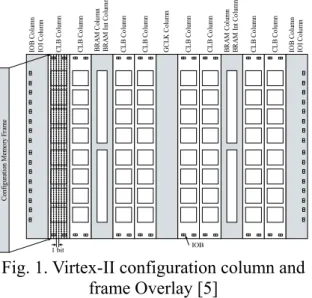
The configuration FPGA means to writing bitstream into configuration memory of FPGA. Bitstream include the logic configuration and the data information inside FPGA. As shown in Fig. 1 [5], the configuration memory frame is organized by a rectangular form which is 1-bit width expanded on entire FPGA column. The frame is the smallest addressable unit of the configuration memory that is loaded to FPGA by column-base. The frame length and number in every column decide upon the series of FPGA. Here, we use XC2V1000 which has 106 words per frame
CLB Column CLB Column
IOB Column IOI Column CLB Column CLB Column
BRAM Column BRAM Int Column CLB Column CLB Column
GCLK Column CLB Column CLB Column
BRAM Column BRAM Int Column IOB Column IOI Column
Configuration Memory Frame
1 bit IOB
Fig. 1. Virtex-II configuration column and frame Overlay [5]
length and 22 frames per CLB column to implement our proposed system. The kinds of frame are separated into IOB, IOI, CLB, BRAM, BRAM_INT and GCLK, as shown in Fig. 1. Each kind of column leads different amount of frames per column [5][6].
A. The Frame Addressing
The frame address use 32-bit. Each frame address is divided into major address (MJA), minor address (MNA) and block address (BA), as shown in TABLE I. Figure 2 shows the Virtex-II configuration memory map.
The MJA decides the specific column in the configuration memory, and is arranged by the column base in FPGA. The n is the number of existing CLB column and the m is the number of existing BRAM column.
The MNA is related to the location of the frame in the column. The BA represents column type in the configuration memory.
B. The Configuration Registers
The configuration logic is saved and controlled by a 32-bit register which is c a l l e d c o n f i g u r a t i o n r e g i s t e r. A l l configurations (configuration or Readback) configure through reading or writing the configuration register data [5]. The configuration registers consist of the CRC
TABLE I. Frame address for Virtext-II FPGA
BA MJA MNA Byte
Number Bits 31-27 26-25 24-17 16-9 8-0
Content 0 x x x 0
0 0
0 1
0 2
0 3
0 4
0 5
0 n + 2
0 n + 3
0 n + 4
1 0
1 m
2 0
2 m Column
Type
BA
MJA
GLCK IOB IOI CLB CLB CLB CLB IOI IOB BRAM BRAM BRAM INT BRAM INT
Fig.2. Column-Level (MJA) configuration memory map [5]
(Cyclic Redundancy Check) register, command register (CMD), frame data input register (FDRI), frame data output register (RDRO), frame address register (FAR) and so on. The CRC register supplies the data input to check error by mechanism in [7][8].
The CMD register is indicated configuration logic and global signal, and to execute other configuration function. There are commands of SHUTDOWN, GCAPTURE, RCFG START and so on. The configuration data is written into configuration memory by moving the frame to the FDRI register. The FDRO is for read/write configuration data or for capture data from FPGA. The operation of reading/writing is pipelined by the frame buffer. Therefore, the smallest FDRI/FDRO read/write operation requires two frames data. The FAR register is to assign the configuration frame address when writing data to FDRI or reading data from FDRO.
IV. Proposed Hardware Context Switching
Because of the ability of hardware context switching in the reconfigurable system that can suspend the program and restart program again, we proposed the architecture of hardware context saving and restoring.
The configuration memory data of FPGA by SelectMAP interface is read, and those frames include the register information.
From the logic allocation file (.ll), we can directly detect and record the frame addresses of these registers in order to reduce the computation time for frame addresses. We find out the same frame addresses and save one of them and this step can reduce the storage space of the frame addresses. Our proposed method is not necessary to modify the hardware task circuit or increase extra access circuit outside the hardware task module. This method is suitable for all hardware task modules and won’t be limited by the behavior of hardware.
A. Context Switching Architecture
Our proposed method for the hardware context switching is able to read back the bitstream arbitrarily by the configuration port of FPGA. Therefore, the hardware context can be obtained and saved by using Readback when the hardware is needed to swap-out. The hardware context will be restored again when the hardware is needed to swap-in. Consequently, the original swapped hardware can continue to accomplish previous works. We control SelectMAP interface for hardware context switching in the dynamically partially reconfigurable system.
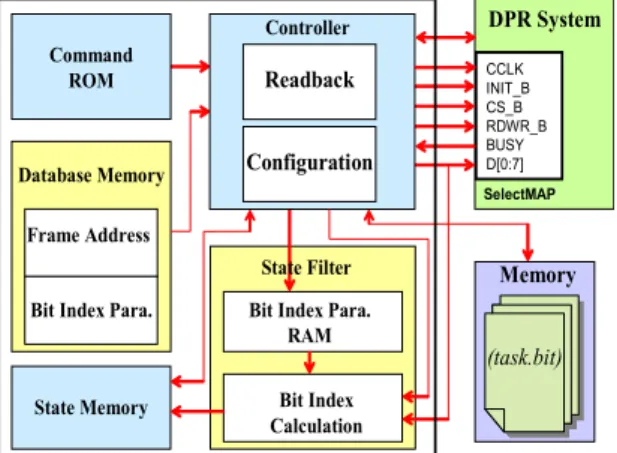
The system architecture of the hardware context switching is shown in Fig. 3. The
DPR System
CCLK INIT_B CS_B RDWR_B BUSY D[0:7]
SelectMAP
(task.bit) Memory Database Memory Controller
Frame Address Bit Index Para.
Command ROM
Bit Index Para.
RAM
Bit Index Calculation State Memory
Configuration Controller Readback
State Filter
Fig. 3. Context switching architecture
system includes five modules: command ROM, database memory, state memory, controller of Readback and configuration, state filter and bitstream memory. The command ROM stores the commands of controlling SelectMAP. The database memory saves frame addresses and parameters of bit indexes that record the locations of hardware task registers. Before the hardware module is swapped out, the state memory saves the register information that filtered from the state filter. The state filter includes the RAM for storing bit index parameters and the bit index calculation unit.
The RAM of state filter temporarily saves the bit index parameters of second frame from the database memory while both registers in one slice have been used. The bit index is used to filtering the register location when reading frames. The controller is used to handle all flows which include Readback, configuration through SelectMAP interface.
B. Context Generation
The frame addresses and the bit indexes of used registers can be found in the logic allocation file. They are important information for building the context database. Figure 4 shows the generation flow of context database. Firstly, we generate the “task.ll” file by BitGen (bitstream generator) and use the editor to parse the register information in the logic allocation file. Next, frame addresses and bit index parameters of registers are built in database memory. Each frame address has
Task Registers Database Logic Allocation
File (task.ll)
Registers Parse
BitGen
Frame Addresses/
Bit Index Para.
Task
Fig. 4. Context generation flow
32-bit data and all registers only occupy two frame addresses in one CLB column.
However, when building the database memory we do not need to save all frame addresses and bit indexes.
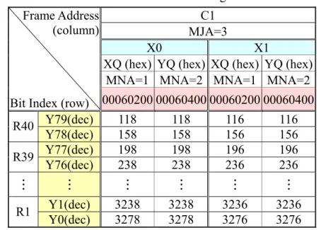
C. Database Memory and State Filter One CLB is composed of four similar slices. One slice has two registers that are XQ and YQ. Therefore, there are 8 registers in one CLB [5]. We arranged the relation of rows, columns, frame addresses and bit index parameters (Y_row) according to the logic allocation file, as shown in TABLE II.
Each column can be separated into two categories, one is even column (X_even) and the other is odd column (X_odd). Each row can be separated into two kinds of rows (Y_even, Y_odd, totally named Y_row). For example, the register occupies two frame addresses in C1 column that are 00060200(hex) and 00060400(hex).
TABLE II is utilized to derive the MJA of the frame address of the register which is shown as equation (1). The MNA value depends on XQ and YQ. If MNA value is 1 then mean using XQ register. If MNA value is 2 then mean using YQ register in design.
There are 32 CLB columns in XC2V1000 and then the maximum MJA=32+2 (This could be known in Fig. 2). Therefore, when
building database memory for the frame address, we use 6-bit to save the MJA and 2-bit to save the MNA.
3 2 / ) 1 _
(
3 2 / _
+
−
=
+
=
odd X
even X
MJA (1)
From TABLE II, we can get some rules of the bit indexes of registers in the frame. For example, there are 8 registers in the C1R40 (column 1, row 40) CLB, and these register data are distributed over bit indexes of 118, 158, 116 and 156. We derive equation (2) from these rules while the column number is odd. Similarly, we derive equation (3) if the column number is even.
) _ 79 ( 40 116 _
_
_bit idx Xodd Y row
fm = + × − (2)
) _ 79 ( 40 118 _
_
_bit idx Xeven Y row
fm = + × − (3)
From equations (2) and (3), we know that the bit indexes are related to the row number of CLB. Hence, we build database memory that only stores the data of Y_row instead of the bit index. The XC2V1000 FPGA has 40 rows and the maximum Y_row is 79 in a CLB column. So we use 7-bit to save Y_row and 1-bit to represent the odd or even column. This bit will be set to "0" when the column number is even and be set "1" when the column number is odd.
When operating Readback procedure to read the frames that only have used registers, the state filter obtains Y_row data from the TABLE II. Frame address and bit Index of registers for XC2V1000
C1 MJA=3
X0 X1
XQ (hex) YQ (hex) XQ (hex) YQ (hex) MNA=1 MNA=2 MNA=1 MNA=2 Frame Address
(column)
Bit Index (row) 00060200 00060400 00060200 00060400
Y79(dec) 118 118 116 116
R40 Y78(dec) 158 158 156 156
Y77(dec) 198 198 196 196
R39 Y76(dec) 238 238 236 236
… … … …
Y1(dec) 3238 3238 3236 3236
R1 Y0(dec) 3278 3278 3276 3276
database memory. Afterward, the bit indexes of registers are calculated by equations (2) and (3), it is useful to filter the data of registers. The register data is saved in the state memory.
D. Frame Addresses and Bit Indexes Addressing
The frame addresses and parameters of bit indexes are saved in the same memory space.
The saving method is to store frame addresses once in the same column (e.g. C1) and continue to store the bit index parameters (Y_row) in the same X column (X_even or X_odd). Moreover, the registers occupied two frame addresses in the same sub-column (e.g. X0) and adjacent locations.
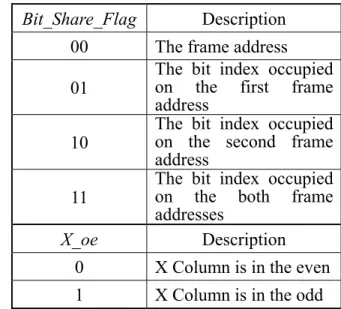
The saving format of database memory has 10-bit, as shown in TABLE III. The 10-bit data use first 2-bit, Bit_Share_Flag, to represent the saved information that is frame address format or bit index parameter format. If the data format is the frame address format, the other 8-bit data has 6-bit for MJA, and 2-bit for MNA. Otherwise, we use 7-bit to save Y_row and 1-bit to save X_oe for the bit index parameter. When the Bit_Share_Flag is represented bit index parameter format which will be used for expressing whether the Y_row sharing to the second frame, and use X_oe to represent the column number is odd (X_odd) or even (X_even), as shown in TABLE IV.
TABLE III. Frame address and bit index parameter of register addressing
Frame Address
Bit_Share_Flag MJA MNA
9 8 7 6 5 4 3 2 1 0
0 0 X X X X X X X X
Bit Index Parameter
Bit_Share_Flag X_oe Y_row
9 8 7 6 5 4 3 2 1 0
X X X X X X X X X X
E. Controller of Readback and Configuration
The controller serves Readback and configuration through SelectMAP interface that is the core of our context switching system. Moreover, database memory, state memory, state filter, bitstream memory and command ROM is also dominated by the controller. The command ROM saves some operating commands for SelectMAP interface.
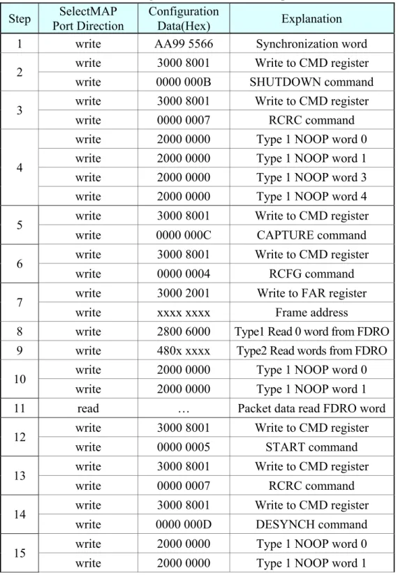
For reading configuration memory, we must send commands into the FPGA to instruct the address and the amount of reading. The operation of Readback means reading frames from the FDRO register. For capturing the states of internal registers, we must use CAPTURE command. The Readback procedure is shown in TABLE V, and the steps are listed as follows:
Step 1: Use the synchronization word to synchronize configuration logics.
Step 2: Set the SHUTDOWN command to suspend the internal action of the hardware module.
Step 3: Set the RCRC command to reset the CRC register.
Step 4: Write four NOOP words to confirm SHUTDOWN procedure which has already been finished.
TABLE IV. The community of bit index and frame address in the register
Bit_Share_Flag Description 00 The frame address 01 The bit index occupied
on the first frame address
10 The bit index occupied on the second frame address
11 The bit index occupied on the both frame addresses
X_oe Description 0 X Column is in the even 1 X Column is in the odd
TABLE V. Setting commands of Readback procedure Step SelectMAP
Port Direction
Configuration
Data(Hex) Explanation 1 write AA99 5566 Synchronization word
write 3000 8001 Write to CMD register
2 write 0000 000B SHUTDOWN command
write 3000 8001 Write to CMD register
3 write 0000 0007 RCRC command
write 2000 0000 Type 1 NOOP word 0 write 2000 0000 Type 1 NOOP word 1 write 2000 0000 Type 1 NOOP word 3 4
write 2000 0000 Type 1 NOOP word 4 write 3000 8001 Write to CMD register
5 write 0000 000C CAPTURE command
write 3000 8001 Write to CMD register
6 write 0000 0004 RCFG command
write 3000 2001 Write to FAR register
7 write xxxx xxxx Frame address
8 write 2800 6000 Type1 Read 0 word from FDRO 9 write 480x xxxx Type2 Read words from FDRO
write 2000 0000 Type 1 NOOP word 0 10 write 2000 0000 Type 1 NOOP word 1
11 read … Packet data read FDRO word
write 3000 8001 Write to CMD register
12 write 0000 0005 START command
write 3000 8001 Write to CMD register
13 write 0000 0007 RCRC command
write 3000 8001 Write to CMD register
14 write 0000 000D DESYNCH command
write 2000 0000 Type 1 NOOP word 0 15 write 2000 0000 Type 1 NOOP word 1 Step 5: Set the CAPTURE command to
read the present state of the register.
Step 6: Set the RCFG command. This is a read command from the FDRO.
Step 7: Set the FAR register to write the initial address of reading.
Step 8: Set the reading word count in Type1 from FDRO.
Step 9: Set the reading word count ijn Type2 from FDRO.
Step 10: Write two NOOP words to flush packet buffer.
Step 11: Start reading configuration data Step 12: Set START command to begin
the start-up sequence.
Step 13: Set the RCRC command to reset the CRC register
Step 14: Set DESYNCH command to desynchronize SelectMAP interface.
Step 15: Write two NOOP words to flush packet buffer.
F. Efficiency analysis
Because of reading one frame address needs one pad frame reading time for flushing the frame buffer. Therefore, operating Readback procedure to read two frame addresses needs four frames reading time that consist of two register frames and two pad frames. So, we only save the former frame address instead of both frame addresses. We can set address to read the former frame, after that will read out three frames that include two register frames and one pad frame. This method can reduce used commands, storage space of one frame address and one pad frame reading time comparing with the Koester’s [2] methods as shown in Fig. 5.
Kalte [1] used 19-bit to save each state register. These saved data are calculated for the frame addresses and bit indexes in the operation of Readback. Afterward, the data of registers are filtered out for saving.
However, our method only needs to calculate bit indexes.
The reconfiguration time depends on the SelectMAP frequency and procedures of operation Readback which command includes: SHUTDOWN (NShudow_cm), CAPTURE and RCFG (NCap_Rcfg_cm), read frames (NFar_cm) and START (NStart_cm) as shown in TABLE V. The sequence of read frames is related to the number of used CLB column (Nclb). The time of setting commands (Tread_cm) is shown in (4). The time of reading frames needs to add on Tread_cm and consider the frame length of FPGA (NByte/Frame). The whole time of reading frame (Tread) is shown in (5). The time of configuration is approximately estimated as Tconfig as shown in (6). Then the complete time of reconfiguration task is the summation of Tconfig and Treconfig as shown in (7).
V. Experimental Results We use there the examples, up-counter, LED display control, 16-bit divider and 32-bit divider to demonstrate the benefit of proposed method. We can suspend the operation of hardware task to switch the context. We implement this work on Xilinx XC2V1000 FPGA platform. In up-counter design example, the BitGen (bitstream generator) generates the logic allocation file (.ll) as shown in Fig. 6. Through the logic allocation file, we can observe locations of the used resources in FPGA. We have used 28 registers and 4 frame addresses that are built to database memory, as shown in TABLE VI.
Two NOOP
Frame Data_2 Frame Data_1 Pad Frame_1 Set Word Count
(3 Frames) Frame Address 1
Set FAR
Two NOOP Two NOOP
Pad Frame_2 Frame Address 2
Frame Data_2 Set Word Count
(2Frames) Set FAR Frame Data_1
Pad Frame_1 Set Word Count
(2 Frames) Frame Address 1
Set FAR
4 Frames Time
3 Frames Time
10 Commands 5 Commands
(a) Koester’s [2]
(b) Our proposed
Fig. 5. Comparison of frame address used space
( )
[ ]
SelectMAP
cm Start clb cm Far cm Rcfg Cap cm Shudow cm read
f
N N N
N N
T
_ _
_ _ _
_
4× + + × +
= (4)
cm SelectMAP read
Frame Byte clb
read T
f N
T 3N _
× +
= (5)
SelectMAP Frame Byte clb config
f N
T N ×
= 22
(6)
cm read SelectMAP
Frame Byte clb
config read reconfig
f T N N
T T T
_
25 × +
= +
=
(7)
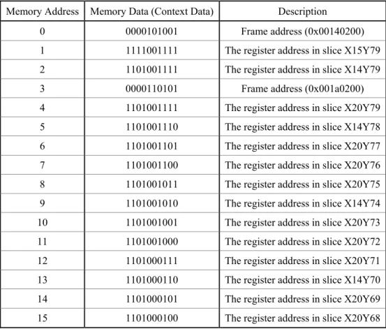
We only need to save two frame addresses to achieve reading data of all registers.
Because of the time of swapping and reconfiguration is an important consideration for the reconfigurable system.
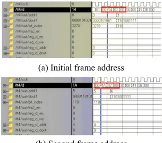
The swap-out simulation of the design example of up-counter is shown in Fig. 7.
The frame address 1, frame address 2 and registers data in Fig. 7 are saved in database memory. The swap-in simulation of up-counter is shown in Fig. 8. The Fig. 8(a) shows bit index places of registers that initial frame address is 0x00140200 and the Fig. 8(b) shows second frame address 0x001a0200 that both are read from database memory. When operating swap-in, the bitstream of up-counter will be downloaded to FPGA again. Therefore, after reading frame addresses, these register values of state memory will be restored to corresponding FPGA registers.
Because of Kalte [1] used the Virtex series FPGA, therefore, we suppose that Kalte’s method [1] needs 18-bit (non 1-bit slice) in Virtex-II FPGA to save the parameters of frame address and bit index
Fig. 6. Logic allocation file of up-counter
Fig. 7. The swap-out simulation of up-counter
TABLE VI. Memory content of up-counter in database
Memory Address Memory Data (Context Data) Description
0 0000101001 Frame address (0x00140200)
1 1111001111 The register address in slice X15Y79
2 1101001111 The register address in slice X14Y79
3 0000110101 Frame address (0x001a0200)
4 1101001111 The register address in slice X20Y79
5 1101001110 The register address in slice X14Y78
6 1101001101 The register address in slice X20Y77
7 1101001100 The register address in slice X20Y76
8 1101001011 The register address in slice X20Y75
9 1101001010 The register address in slice X14Y74
10 1101001001 The register address in slice X20Y73
11 1101001000 The register address in slice X20Y72
12 1101000111 The register address in slice X20Y71
13 1101000110 The register address in slice X14Y70
14 1101000101 The register address in slice X20Y69
15 1101000100 The register address in slice X20Y68
for each register (8-bit x column, 8-bit y row, 1-bit XQ or YQ and 1-bit current state of register). TABLE VII shows the comparison of our method with Kalte’s [1] in memory usage for four different hardware tasks. The memory usage of Kalte’s [1] method linearly increases while ours can be reduced averagely about 49.67%.
Our design examples are implemented on XC2V1000 FPGA. Therefore, the frame length is 424 bytes and the configuration frequency of SelectMAP is 50 MHz. The experimental results are shown in TABLE VIII, we have compared our method with Koester’s [2] in the number of reading frames which include the pad frames. The time of read frame and reconfiguration hardware are calculated, and our proposed method can reduce the time of reconfiguration task average about 4.011%.
VI. Conclusion
A hardware context switching method has proposed to reduce the memory usage for the hardware context switching in the dynamically partially reconfigurable system.
It also can reduce the reading time of one pad frame and setting command complexity in Readback operation. Specially, our architecture is completely implemented by hardware. Comparison of related work, experimental results show that our method can reduce averagely 49.67% of memory used for saving hardware context and 4.011
% of hardware reconfiguration time. In the future, we will extend the management of the priority and schedule of hardware task that will improve resource usage in FPGA.
(a) Initial frame address
(b) Second frame address
Fig. 8. The swap-in simulation up-counter TABLE VII. Comparison of memory size
Methods
Design Examples (Used Flip Flops)
Kalte [1] Ours Reduced
Up-Counter (28) 476 Bits 160 Bits 66.39%
16-bit Divider (40) 680 Bits 420 Bits 38.24%
LED Display
Control (46) 782 Bits 400 Bits 48.85%
32-bit Divider (73) 1241 Bits 680 Bits 45.21%
Average 49.67%
TABLE VIII. Comparison of reconfiguration time for saving and restoring context Design Examples Up-Counter LED Display Control 16-bit Divider 32-bit Divider
Method Koester [2] Ours Koester [2] Ours Koester [2] Ours Koester [2] Ours
Total Frames to Read 8 6 36 27 40 30 56 42
Read Data (Byte) 3392 2544 15264 11448 16960 12720 23744 17808
Command (Byte) 164 124 444 264 484 284 644 364
Command Time( ) 3.28 2.48 8.88 5.28 9.68 5.68 12.88 7.28 Read Time( ) 71.12 53.36 314.16 234.24 348.88 260.08 48.76 363.44 Reconfig. Time( ) 444.24 426.48 1933.2 1913.28 2205.38 211.58 3099.6 2975.28
Reduced Treconfig 3.9978% 4.0096% 4.0265% 4.0108%
Average 4.011175%
References
[1] H. Kalte and M. Porrmann, “Context Saving and Restoring for Multitasking in Reconfigurable Systems,” in International Conference on Field Programmable Logic and Applications, pp. 223-228, Aug. 24-26, 2005.
[2] M. Koester, M. Porrmann and H. Kalte,
“Relocation and Defragmentation for Heterogeneous Reconfigurable System,”
in International Conference on Engineering of Reconfigurable Systems and Algorithms, pp. 70-76, Jun. 26-29, 2006.
[3] S. Guccione, D. Levi and P. Sundararajan,
“JBits: A Javabased interface for reconfigurable computing,” in 2th Annual Military and Aerospace Applications of Programmable Devices and Technologies Conference (MAPLD), pp.
253-261, September 1999.
[4] H. Simmler, L. Levinson and R. Manner,
“Multitasking on FPGA Coprocessors,”
in 10th International Workshop on Field
Programmable Gate Arrays (FPL), pp.
121-130, Aug. 27-30, 2000.
[5] Xilinx, Inc. “Virtex-II platform FPGA user guide,” Xilinx UG002, March 23, 2005.
http://direct.xilinx.com/bvdocs/userguide s/ug002.pdf
[6] M. Hubner, C. Schuck and J. Becker,
“Elementary block based 2-dimensional dynamic and partial reconfiguration for Virtex-II FPGAs,” in 20th International Parallel and Distributed Processing Symposium (IPDPS), pp. 8, April 25-29, 2006.
[7] Xilinx, Inc. “Virtex series configuration architecture user guide,” Xilinx XAPP151, October 20, 2004.
http://www.xilinx.com/bvdocs/appnotes/
xapp151.pdf
[8] Xilinx, Inc. “Virtex FPGA series configuration and Readback,” Xilinx XAPP138, March 11, 2005.
http://www.xilinx.com/bvdocs/appnotes/
xapp138.pdf
![Fig. 5. Comparison of frame address used space ( )[ ] SelectMAP cmStartclbcmFarcmRcfgCapcmShudowcmreadfNNNNNT______4×++×+= (4) cm SelectMAP readFrameByteclbreadTfNT3N _×+= (5) SelectMAP FrameByteclbconfigfNTN×=22 (6) cmread SelectMAP FrameByteclbconfi](https://thumb-ap.123doks.com/thumbv2/9libinfo/9493124.591939/8.892.462.788.481.1152/comparison-selectmap-cmstartclbcmfarcmrcfgcapcmshudowcmreadfnnnnnt-selectmap-readframebyteclbreadtfnt-selectmap-framebyteclbconfigfntn-framebyteclbconfi.webp)