Wen-Ting Chiou, Wan-Yu Wu, and Jyh-Ming Tinga)
Department of Materials Science and Engineering, National Cheng Kung University, Tainan, Taiwan (Received 15 November 2004; accepted 14 April 2005)
ZnO nanowires along with ZnO thin films were obtained on copper-metallized silicon substrates using an radio frequency-reactive sputter-deposition technique. Residual tensile stresses were found in both the copper layer and the ZnO layer. The ZnO nanowires were observed exclusively at the grain boundaries of the ZnO thin films. The average diameter of ZnO nanowires varies only slightly with the ZnO deposition time, while the average length increases linearly with the ZnO deposition time. Based on the observations a growth model involving stress-assisted diffusion of copper and reaction-controlled catalytic growth of ZnO nanowires is suggested.
I. INTRODUCTION
ZnO nanostructures with excellent optoelectronic properties are useful for light-emitting diode,1,2
semicon-ductor, fluorescence, and optical probe.3 Among the nanostructures, ZnO nanowires and nanorods are usually synthesized using vapor-phase oxidation of metallic Zn powders,4,5vapor phase transport process via catalyzed epitaxial crystal growth,6,7chemical reactions in confine spaces provided by alumina templates with nanochan-nels,8 and aqueous growth method.9 Irrespective of the forms and growth techniques, successful growth of ZnO nanowires and nanorods typically requires the use of a single-crystal substrate, such as sapphire or diamond.
In previous papers, we have reported the growth of ZnO nanowires on a non-single-crystal substrate using a conventional reactive sputter deposition technique.10,11It was found that ZnO nanowires can be grown on copper metallized silicon wafers. However, the copper has to be prepared by electroless plating. The use of other tech-niques such as sputter deposition for the preparation of copper metallization failed to produce ZnO nanowires. Although the presence of a copper layer was found to be decisive in obtaining the ZnO nanowires, correlation of the processing parameters and the growth of ZnO nano-wires is required for further understanding of the growth of ZnO nanowires. As a result, in this study, we have further explored the role of electroless copper by inves-tigating the residual stresses in both the copper and the ZnO thin films, and the preferred growth sites of ZnO nanowires. A formation mechanism based on the consid-eration of the residual stress and copper as the catalyst is discussed
II. EXPERIMENTAL
As-received p-type, (100) silicon wafers were used as virgin substrates. The wafers were first deposited with a thin layer of Ti using a direct current (dc) sputter-deposition technique. The Ti layer is used as a diffusion barrier. The Ti-deposited silicon wafers were electroless-plated with copper. The detailed plating process and the electroless bath composition can be found elsewhere.12 The electroless copper plating was performed in a batch manner. In a batch, four identical Ti-deposited Si cou-pons were immersed in the bath at the same time. The coupons were subsequently removed from the bath one by one after 1, 2, 3, and 4 min of plating time. Substrates thus obtained were then subjected to ZnO deposition in a radio frequency (rf) magnetron-reactive sputter-deposition chamber. The target used was a ZnO target. The rf sputter-deposition chamber was initially evacu-ated to a pressure lower than 5 × 10⁻⁵ Torr. The depo-sition of ZnO was carried out under a working pressure of 5 × 10⁻² Torr, an rf power of 200 W, a working distance of 50 mm, an atmosphere of O2/Ar⳱ 0.3, and
various deposition times of 1, 5, 10, 20, and 30 min. No external substrate heating or bias was applied to the sub-strate during the deposition. The subsub-strates were heated only by the plasma to temperatures near 120 °C as de-termined by a thermocouple. Specimens of electroless copper layers and ZnO deposits were analyzed for crystal structure using x-ray diffractometry (XRD) and for mor-phology using scanning electron microscopy (SEM). Ca-thodic luminescence (CL) was also performed on the ZnO nanowires and the films.
III. RESULTS AND DISCUSSION
As mentioned above, ZnO nanowires can only be ob-tained, along with ZnO thin films, in the presence of an electroless copper layer. In this study, a total of four
a)
Address correspondence to this author. e-mail: [email protected] DOI: 10.1557/JMR.2005.0286
different electroless plating times was used to deposit copper layers on Ti-coated Si substrates. The thickness, surface morphology, grain size, crystallinity, and residual stress of the copper layers were first examined. As seen and discussed below, the characteristics of electroless copper seem to vary to a certain extend from batch to batch, presumably due to the rigorous reaction kinetics that varies from batch to batch; however, clear correla-tions between the copper characteristics and the occur-rence of ZnO nanowires can be obtained. Also, although the plating thickness varies from batch to batch, in gen-eral, the thickness of electroless copper increases from ∼0.2 to ∼1.0 m as the plating time increases from 1 to 4 min. All the copper layers exhibit very rough surfaces where many bumps can be seen. This is due to the evo-lution of hydrogen during the electroless plating. All the copper layers were found to be polycrystalline with a preferred orientation of the (111) plane, as shown in Fig. 1. The peak intensity always increases with the cop-per layer thickness or plating time as a result of increased diffraction volume of copper. Due to the thickness of the copper layer, diffraction peaks of the Ti buffer layer are seen. However, the Ti peak intensity decreases with the copper layer thickness or plating time. There is also a weak peak of Cu2O, indicating minor oxidation of the
copper layers. However, the formation of Cu2O was
minimized by quickly transfer the copper-plated speci-mens to the ZnO deposition chamber. The average grain sizes of the copper layers were calculated form the XRD spectra using the Scherrer equation. The result is com-pared with the average grain sizes measured on SEM micrograph. It was found that the average grain size in-creases with the plating time and the Scherrer equation always predicts smaller grain sizes as shown in Fig. 2. The fact that the average grain sizes determined by the Scherrer equation are smaller indicates the existence of tensile stresses in the copper layers.13 The calculated
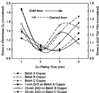
tensile stresses are shown in Fig. 3.14Deposition of ZnO was then performed using substrates plated with various copper layers using different sputter-deposition times.
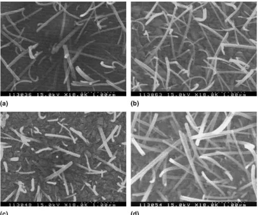
It is found that the ZnO deposits on the copper layers retain the tensile stress as shown in Fig. 3. For each batch of the electroless copper layers, all the 1-, 10-, and 20-min ZnO deposits exhibit tensile stresses whose variations with the plating time are essentially the same as that of the copper layers. The surface morphology of ZnO deposit was examined using SEM. SEM analysis indicates that each deposit consists of a ZnO thin film and nanowires, as shown in Fig. 4. It appears that ZnO nanowires are at the grain boundaries of the ZnO thin film exclusively, as indicated by the circles or ellipses. The ZnO nanowires were subjected to room temperature optical property measurements. The photoluminescence spectra are shown in Fig. 5. The spectra are very similar to the ZnO nanowires prepared using copper as the cata-lyst in a controlling carrying gas flow pattern (CGFP) method.15A strong ultraviolet (UV) emission ∼395 nm
FIG. 1. XRD spectra of electroless copper layers with plating times of (a) 1 min, (b) 2 min, (c) 3 min, and (d) 4 min.⽧ Ti (100), ● Cu2O
(111), * Ti (002),䡩 Ti (101), 〫 Cu (111), 䉮 Cu (002).
FIG. 2. Average grain sizes of copper layers determined using SEM micrograph measurement and XRD spectra.
and weak green emission ∼578 nm were observed. The former is a result of the near-band-edge emission of the wide band gap of ZnO; while latter is possibly due to the singly ionized oxygen vacancies in ZnO.16
It was also observed that the area density (#/m2
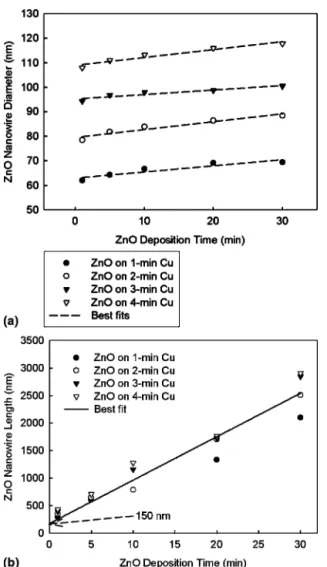
) of ZnO nanowires seems to vary from one specimen to another, as shown in Fig. 6, without an obvious correlation with the copper plating time. In fact, as shown in Fig. 7, the area density cannot be correlated with both the copper plating time and the ZnO deposition time, and therefore the grain sizes. Although Fig. 4 does not suggest a quantitative correlation between the area density and the grain size, very useful information can still be extracted from the observation shown in Fig. 4 as discussed later. On the other hand, a correlation between the ZnO nanowire di-mensions and ZnO deposition time was found. The av-erage diameter of ZnO nanowires varies only slightly with the ZnO deposition time [Fig. 8(a)] while the aver-age length increases linearly with the ZnO deposition time. The linear growth of ZnO nanowires is shown in Fig. 8(b). The interception at time zero was found to be approximately 150 nm, as indicated in the figure.
As a result, a ZnO nanowires growth mechanism, as shown in Fig. 9, involving stress-assisted diffusion of copper and reaction-controlled catalytic growth is sug-gested. In the initial stage, ZnO thin film is formed on the electroless copper layer [Fig. 9(a)]. At this initial stage, there is no formation of ZnO nanowire. As the ZnO deposition proceeds, diffusion of copper into the ZnO FIG. 4. Surface morphology of ZnO deposits on Cu-plated substrate.
FIG. 5. Photoluminescence spectra of ZnO nanowires.
FIG. 8. Variation of ZnO nanowire (a) diameter and (b) length with the ZnO deposition time.
FIG. 9. ZnO nanowire growth model (not to scale): (a) initial stage where only ZnO thin film is formed; (b) second stage where the diffusion of copper through the grain boundaries of ZnO layer occurs due to not only the substrate temperature but also the existence of the stresses; (c) third stage where Cu–Zn alloy particles form; and (d) final stage where the Cu–ZnO particles serve as catalysts for the formation of ZnO nanowires.
FIG. 7. Variations of ZnO nanowire area density with the ZnO depo-sition time and the copper plating time.
layer is believed to take place. In Cu/ZnO/Zn specimens, diffusion of copper through ZnO was reported at a tem-perature of 400 K.17The diffusion is suggested to be a grain-boundary diffusion. After the copper diffused through the ZnO layer, it formed Cu–Zn alloys with the Zn layer. In this study, the substrate temperature was approximately 120 °C, which is near 400 K. The sub-strate temperature then provides a desirable condition for copper diffusion through the grain boundaries of ZnO thin film. Also the existence of tensile stresses in both the copper layers and the ZnO layers (Fig. 3) would further make such diffusion possible.18 The existence of the stresses is considered to be of critically important. It is noted that the stress relationship shown in Fig. 3 was not observed for copper prepared by other physical vapor-deposition methods;10,11and therefore, under such a cir-cumstance, there was no formation of ZnO nanowires. As a result, in the second stage [Fig. 9(b)] the electroless copper diffuses through the grain boundaries of ZnO layer. Upon reaching the surface of ZnO film, the copper precipitates to form particles, which are then exposed to the plasma where oxygen and zinc can be found. As the oxidation of copper is not favored in the presence of Zn due to thermodynamic consideration,19 the copper particles then serve as the catalyst for the growth of ZnO nanowires. It is noted that the use of catalyst, such as Au and Cu, for the formation of ZnO nanowires has been reported.6,20–23 The copper particles catalyze the oxidation reaction of Zn to form ZnO nanowires as the deposition continues [Fig. 9(d)]. At this stage, the formation of ZnO nanowires is through a first-order reaction-controlled process. Due the negligible thicken-ing (Fig. 8), the reaction kinetics is described as
dL
dt = kC ,
where L is the length, t the reaction time, k the reaction constant, and C the concentration. The concentration is a constant in this study. Integration of the above equation therefore gives
L⳱ L0+ kCt .
This describes the best fit shown in Fig. 8(b). According to the best fit, L0⳱ 150 nm. As mentioned above, the
thickening of ZnO nanowires is negligible. Therefore, the diameter of the nanowire is thought to approximate the initial Cu particle size. From Fig. 8(a), the initial Cu particle diameter ranges from 60 to 120 nm. The value of L0 approximates this range. This supports our argument
that the formation of a ZnO nanowire starts with a cata-lyst particle. Finally, the last stage, as shown in Fig. 9(d), also depicts the formation of ZnO nanowires at the grain boundaries as shown in Fig. 4.
IV. CONCLUSIONS
The use of copper-metallized silicon substrate for the deposition of ZnO in an rf sputter-reactive deposition chamber results the formation of not only ZnO thin films but also selected area growth of ZnO nanowires on the ZnO thin film. The growth of ZnO nanowires was found exclusively at the grain boundaries of the ZnO thin films. Although a quantitative correlation between the area den-sity of ZnO nanowires and the grain size of ZnO thin film was not observed, the fact that ZnO nanowires were only found at the grain boundaries and the existence of re-sidual stresses in both the copper and ZnO layers has led a suggested growth model. The model involves stress-assisted diffusion of copper through the grain boundaries of ZnO thin film and catalytic growth of ZnO nanowires. The growth of ZnO nanowires was linear and determined to be a first-order reaction-controlled process.
ACKNOWLEDGMENTS
This work was supported by the National Science Council in Taiwan (Grant NSC 93-2120-M-006-007) and the Department of Education in Taiwan (Grant 91-E-FA09-5-4). The use of the equipment in the Micro-Nano Technology Research Center in the National Cheng Kung University is also acknowledged.
REFERENCES
1. M.H. Huang, S. Mao, H. Feick, H. Yan, Y. Wu, H. Kind, E. Weber, R. Russo, and P. Yang: Room-temperature ultraviolet nanowire nanolasers. Science 292, 1897 (2001).
2. B.J. Jin, S.H. Bae, S.Y. Lee, and S. Im: Effects of native defects on optical and electrical properties of ZnO prepared by pulsed laser deposition. Mater. Sci. Eng. B 71, 301 (2000).
3. C. Pieralli and M. Hoummady: New optical probe using ZnO whiskers: Analyses. of sub-wavelength dithering and evanescent wave propagation. Appl. Phys. A 66, S377 (1998).
4. Z. Zhou, H. Deng, J. Yi, and S. Liu: A new method for preparation of zinc oxide whiskers. Mater. Res. Bull. 34, 1563 (1999). 5. Z. Zhou, W. Peng, S. Ke, and H. Deng: Tetrapod-shaped ZnO
whisker and its composites. J. Mater. Process. Tech. 89–90, 415 (1999).
6. Y.W. Wang, L.D. Zhang, G.Z. Wang, X.S. Peng, Z.Q. Chu, and C.H. Liang: Catalytic growth of semiconducting zinc oxide nanowires and their photoluminescence properties. J. Cryst.
Growth 234, 171 (2002).
7. M.H. Huang, Y. Wu, H. Feick, N. Tran, E. Weber, and P. Yang: Catalytic growth of zinc oxide nanowires by vapor transport. Adv.
Mater. 13, 113 (2001).
8. Y. Li, G.W. Meng, L.D. Zhang, and F. Phllipp: Ordered semicon-ductor ZnO nanowire arrays and their photoluminescence proper-ties. Appl. Phys. Lett. 76, 2011 (2000).
9. L. Vayssieres, K. Keis, A. Hagfeldt, and S.E. Lindquist: Three-dimensional array of highly oriented crystalline ZnO microtubes.
Chem. Mater. 13, 4395 (2001).
10. Y.S. Chang and J.-M. Ting: Growth of ZnO thin films and whis-kers. Thin Solid Films 398–399, 29 (2001).
ZnO nanowires using sputter deposition. Diamond Relat. Mater. 12,1841 (2003).
12. Y.S. Chang: Deposition of ZnO on copper metallized silicon wa-fers. Master’s Thesis, National Cheng Kung University, Taiwan, 2000.
13. B.D. Cullity: Elements of X-Ray Diffraction (Addison-Wesley Pub. Co., Reading, MA, 1978).
14. Stress analysis, in X-ray Diffraction Handbook (in Japanese) (Rigaku Co., Tokyo, Japan, 1998), Chap. 3.
15. S.Y. Li, P. Lin, C.Y. Lee, and T.Y. Tsenga: Field emission and photofluorescent characteristics of zinc oxide nanowires synthe-sized by a metal catalyzed vapor–liquid–solid process. J. Appl.
Phys. 95(7), 3711 (2004).
16. K. Vanheusden, W.L. Warren, C.H. Seager, D.R. Tallant, J.A. Voigt, and B.E. Gnade: Mechanisms behind green photolu-minescence in ZnO phosphor powders. J. Appl. Phys. 79, 7983 (1996).
17. K.R. Harikumar, A.K. Santra, and C.N.R. Rao: An investigation of the Cu/ZnO/Zn system: Evidence for the formation of Cu–Zn alloys by the inward diffusion of Cu. Appl. Surf. Sci. 93, 135 (1996).
18. P. Shewmon: Diffusion in Solids, 2nd ed. (Minerals, Metals & Materials Society, Warrendale, PA, 1989).
19. E. Kubaschewski, L.L. Evans, and C.B. Alcock: Metallurgical
Thermochemistry, 4th ed. (Pergamon Press, New York, 1967).
20. M.H. Hwang: Room-temperature ultraviolet nanowire nanolasers.
Science 292, 1897, (2001).
21. P. Yang: Controlled growth of ZnO nanowires and their optical properties. Adv. Funct. Mater. 12(5), 323 (2002).
22. S.C. Lyu: Low temperature growth and photoluminescence of well-aligned zinc oxide nanowires. Chem. Phys. Lett. 363, 134 (2002).
23. S.Y. Li: Copper-catalyzed ZnO nanowires on silicon (100) grown by vapor–liquid–solid process. J. Cryst. Growth 247, 357 (2003).