Effect of growth temperature on a-plane ZnO formation on r-plane sapphire
Chun-Yen Peng, Jr-Sheng Tian, Wei-Lin Wang, Yen-Teng Ho, Shu-Chang Chuang, Ying-Hao Chu, and Li Chang
Citation: Journal of Vacuum Science & Technology A 29, 03A110 (2011); doi: 10.1116/1.3549141
View online: http://dx.doi.org/10.1116/1.3549141
View Table of Contents: http://scitation.aip.org/content/avs/journal/jvsta/29/3?ver=pdfcov
Published by the AVS: Science & Technology of Materials, Interfaces, and Processing
Articles you may be interested in
Growth and structural properties of ZnO films on ( 10 10 ) m -plane sapphire substrates by plasma-assisted molecular beam epitaxy
J. Vac. Sci. Technol. B 27, 1625 (2009); 10.1116/1.3119682
Growth of nonpolar ( 11 2 ¯ 0 ) ZnO films on LaAlO 3 (001) substrates
Appl. Phys. Lett. 93, 121911 (2008); 10.1063/1.2988167
Second and third order nonlinear optical properties of microrod ZnO films deposited on sapphire substrates by thermal oxidation of metallic zinc
J. Appl. Phys. 102, 113113 (2007); 10.1063/1.2822461
Effects of ZnO buffer layers on the fabrication of GaN films using pulsed laser deposition
J. Appl. Phys. 101, 093519 (2007); 10.1063/1.2730573
Epitaxial growth and surface modeling of ZnO on c -plane Al 2 O 3
Chun-Yen Peng, Jr-Sheng Tian, Wei-Lin Wang, Yen-Teng Ho, Shu-Chang Chuang, Ying-Hao Chu, and Li Changa兲
Department of Materials Science and Engineering, National Chiao Tung University, Hsinchu, Taiwan 300, Republic of China
共Received 10 September 2010; accepted 3 January 2011; published 1 March 2011兲
The effect of growth temperature on a-plane ZnO formation on r-plane sapphire has been systematically investigated by employing in situ high pressure reflection high-energy electron diffraction, atomic force microscopy, and high-resolution x-ray diffraction. For film growth above and below 600 ° C, it is shown that there is a significant difference in growth rate and surface morphology due to the differences in the growth mode. Stripelike morphologies were observed on the surface of a-plane ZnO grown at low temperature共LT兲 because of differences in the growth rate along the c-axis and the growth rate normal to the c-axis. Furthermore, annealing of films grown at low temperature results in more pronounced stripe morphology and in improvement of crystallinity. © 2011 American Vacuum Society. 关DOI: 10.1116/1.3549141兴
I. INTRODUCTION
Zinc oxide, a semiconductor with a hexagonal wurtzite structure 共P63mc, a = 3.213 Å, and c = 5.213 Å兲,1 has
ceived much attention in the past decade because of its re-markable optical properties, which include a wide direct band gap and large excitonic binding energy. These proper-ties make ZnO attractive for applications in optoelectronic devices such as light emitting diodes and laser diodes. Though the growth of high quality c-plane共0001兲 crystalline ZnO has already been successfully achieved,2–4 it is well established that the built-in electrostatic field caused by pi-ezoelectric polarization in wurtzite structure lowers the car-rier recombination efficiency and degrades the optical emis-sion properties. In order to avoid the so-called quantum confined Stark effect, nonpolar films without polarity along the growth direction are required. Hence, nonpolar a-plane and m-plane ZnO film growth has been intensively studied in recent years.
Sapphire is a commonly used substrate for growth of ep-itaxial optoelectronic thin films such as GaN, AlN, and ZnO. Srikant et al.5 reported the epitaxial relationships of ZnO films grown on various orientation sapphire substrates in-cluding a-plane共112¯0兲, m-plane 共11¯00兲, c-plane 共0001兲, and r-plane 共11¯02兲 sapphire. Epitaxial orientation relationships for the growth of polar c-plane ZnO films on c-plane and on a-plane sapphire have been established. Also, nonpolar a-plane ZnO films have been successfully grown on r-plane sapphire. These films had a pure a-plane orientation, and the x-ray rocking curves exhibited a full width at half maximum 共FWHM兲 of 0.72° –0.95° when the growth temperature was above 650 ° C. However, the epitaxial orientation changed to 共0001兲ZnO 储共11¯02兲sapphire when the growth temperature was
below 550 ° C.
provement on the crystalline quality of these films. Though high crystalline quality a-plane ZnO films can be obtained by plasma-assisted molecular-beam epitaxy共MBE兲,9,10its qual-ity is still not comparable to that of a-plane GaN on r-sapphire even though these systems have similar lattice mismatch.11,12
To improve the crystallinity, it is essential to understand the growth evolution and surface morphology, which may depend on various deposition parameters. Pulsed laser depo-sition共PLD兲 is well established to grow high-quality epitax-ial ZnO films on sapphire. Among experimental conditions for PLD of ZnO on sapphire, the thickness and growth tem-perature play important roles in determining the film quality. The advantage of using PLD for ZnO growth is that in situ reflection high-energy electron diffraction can be used to monitor the surface conditions during growth. Here, using reflection high-energy electron diffraction, high-resolution x-ray diffraction 共HRXRD兲, and atomic force microscopy 共AFM兲, we show that a-plane ZnO growth on r-sapphire by PLD at different substrate temperatures can result in a sig-nificant variation of ZnO growth rate, crystallinity, and sur-face morphology.
II. EXPERIMENT
ZnO films were grown on 8⫻8 mm2 r-plane sapphire
wafers in a Pascal laser-MBE system equipped with a KrF excimer laser and a high pressure reflection high-energy electron diffraction 共RHEED兲 apparatus. The sapphire sub-strates were cleaned using acetone in the ultrasonic bath, followed by thermal cleaning in vacuum of at 850 ° C and 10−6 torr. Thin films of ZnO were grown at temperatures
ranging from 350 to 850 ° C with 10 mtorr oxygen partial pressure.
operated in AFM tapping mode. All the X-ray experiments were performed on a Philips X’Pert Pro 共MRD兲 diffracto-meter employing a graded parabolic x-ray mirror and a Ge 共220兲 monochromator.
III. RESULTS AND DISCUSSION
The thickness and growth rates of ZnO after 1200 laser pulses at temperature ranging from 350 to 850 ° C on r-plane sapphire substrates are shown in Fig.1. Figure 1共a兲 clearly shows that the film thickness measured by XRR decreases with growth temperature even though these samples were grown using the same number of pulses and under otherwise the same deposition conditions. From 350 to 550 ° C, the thickness slightly decreases from about 29 to 26 nm, but it significantly decreases to about 18 nm at 650 and 750 ° C. The thickness of the film deposited at 850 ° C is about 8 nm, which indicates a significant reduction in the growth rate with deposition temperature, as shown in Fig.1共b兲. Several studies had reported that stoichiometric sublimation of ZnO takes place at an appreciable rate above 600 ° C under ultra-high vacuum conditions due to removal of lattice oxygen from the lattice.13–15Thus, it is likely that the lower growth rate at high temperatures might be due to the desorption and decomposition of ZnO. The corresponding surface roughness of the deposited films is shown in Fig.1共c兲. All films
depos-ited after 1200 pulses have a root-mean-square 共rms兲 value below 0.8 nm, suggesting that all the film surfaces are very smooth.
Figure 2 shows the surface morphology of 10 nm thick ZnO films deposited at 450, 750, and 850 ° C. Figure 2
shows that the surface roughness increases from 0.35 nm for the film deposited at 450 ° C to 0.78 nm for the film depos-ited at 850 ° C. The AFM images in Figs.2共d兲–2共f兲show that stripelike morphology can be recognized on the surface of the films deposited at low temperature 共LT兲, while no such characteristics can be seen on the surface of the film depos-ited at 850 ° C. The corresponding in situ RHEED patterns of these 10 nm thick films are shown in Figs.2共a兲–2共c兲. All the patterns exhibit periodic reflections, indicating that the a-plane ZnO films deposit epitaxially on the r-plane sapphire. In the RHEED pattern of the film deposited at 450 ° C, long and streaky lines can be clearly seen, indicating that the film has a smooth surface consistent with the AFM observation in Fig. 2共f兲. However, more spotty reflections are observed in the pattern exhibited by the film deposited at 850 ° C because of its rough surface. Moriyama and Fujita16reported similar observations, showing that the morphology consists of three-dimensional 共3D兲 islands when growth is at 800 °C and is stripelike at 500 ° C. These results suggest that low-temperature deposition may lead to a larger flat surface, while high-temperature 共HT兲 deposition may favor island growth in the initial stages.
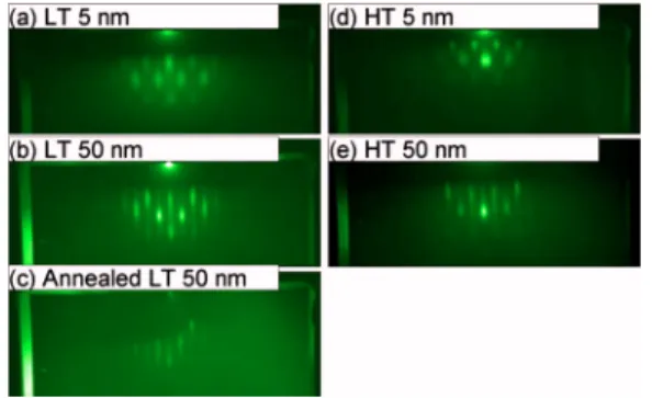
To understand the surface evolution, we have done a se-ries of in situ RHEED observations during growth. Figure3
shows the RHEED patterns of ZnO taken with electron beam incident along ZnO关0001兴 after film growth at 450 °C 共des-ignated as LT兲 and after film growth at 750 °C HT. After growth of ZnO in 5 nm thickness on r-plane sapphire in the temperature range 350– 850 ° C, ZnO exhibits a 3D island structure as Figs.3共a兲and3共d兲show spotty reflections in the RHEED patterns. After growing 50 nm thick films, the re-flections in both LT and HT RHEED patterns become streaky lines, suggesting that the surface smoothness is improved. Similar results have been reported previously and it was shown that the surface exhibits a 3D island structure at the beginning of the growth, while further growth can make the surface smoother due to the lateral growth.16,17
FIG. 1. 共Color online兲 Variation of ZnO films of 共a兲 thickness, 共b兲 growth rates, and共c兲 surface roughness with growth temperature. The number of applied laser pulses for all deposition conditions was 1200.
FIG. 2. 共Color online兲 关共a兲–共c兲兴 RHEED patterns and 关共d兲–共f兲兴 AFM images of 10 nm ZnO films grown at 关共a兲 and 共d兲兴 850, 关共b兲 and 共e兲兴 750, and 关共c兲 and 共f兲兴 450 ° C.
Peng et al.: Effect of growth temperature on a-plane ZnO formation
03A110-2 03A110-2
The AFM images of 50 nm thick LT and HT grown ZnO films are shown in Figs. 4共a兲 and4共c兲. These figures show that the LT ZnO exhibits stripelike morphology, whereas the HT ZnO films do not show these striped features. The fact that there is a morphology difference between LT and HT ZnO films supports the conclusion reached based on the thickness measurement shown in Fig.1that low temperature growth mode of a-plane ZnO is different from that at high temperature. Anisotropic diffusion rate and large strain due to anisotropic lattice mismatch between ZnO c-axis and m-axis may result in anisotropic growth of a-plane ZnO be-tween parallel and perpendicular to the c-axis at low temperature.18 For high temperature growth, the large aniso-tropic strain might be relaxed and surface diffusion might be similar at both directions, resulting in the growth rate parallel to the c-axis being not significantly different than that per-pendicular to the c-axis. As a result, the surface morphology exhibits the step-terrace characteristics when the film thick-ness is 50 nm. The roughthick-ness measurements by AFM show that the 50 nm HT thick film has a roughness of 0.4 nm, smaller than 0.6 nm, the value for the 17 nm thick HT film 关Fig.1共c兲兴.
Interestingly, if the 50 nm thick LT film is directly an-nealed at 750 ° C for 10 min with oxygen pressure of 1 ⫻10−2 torr in the PLD chamber, the characteristics in the
RHEED pattern shown in Fig. 3共c兲 are nearly the same as that obtained from the film that was not annealed关Fig.3共b兲兴,
implying that the surface structure remains unchanged and the surface smoothness is similar in the direction of the elec-tron beam. However, the AFM image in Fig.4共b兲reveals that
the surface evolves into more pronounced stripe morphology as the stripe width increases to ⬃80–100 nm after anneal-ing. This is in comparison to width共⬃50 nm兲 before anneal-ing. This result suggests that increasing the deposition tem-perature may enhance the diffusion and lateral growth perpendicular to the c-axis.
Figure5共a兲shows x-ray 2/ patterns from 50 nm thick LT and HT grown ZnO films. Clearly, only r-plane sapphire and 共112¯0兲ZnO peaks are seen at 54.5° and 56.5°, respec-tively, without a visible 共0002兲 ZnO peak. The 共112¯0兲ZnO
XRCs shown in Figs.5共b兲–5共d兲illustrate that the FWHM of the HT film is 0.625° in the direction parallel to the c-axis and 1.314° in the direction normal to the c-axis. For the LT film, the FWHM is 0.5° in the direction parallel to the c-axis and 0.7° in the direction normal to the c-axis. Thus, low-temperature growth can result in better film crystallinity. Fur-ther annealing of the LT film at 750 ° C for 10 min can improve the film crystallinity as the FWHM of the XRC decreases to 0.44° in the direction parallel to the c-axis and 0.67° in the direction normal to the c-axis.
FIG. 3. 共Color online兲 In situ RHEED patterns of ZnO taken with electron beam incident along ZnO关0001兴 after various film growth conditions. 共a兲 After growth of 5 nm thick ZnO at 450 ° C.共b兲 After growth of 50 nm ZnO at 450 ° C and共c兲 after further direct annealing at 750 °C in 1⫻10−2 torr O2.共d兲 After direct growth of 5 nm thick ZnO on sapphire and 共e兲 50 nm ZnO at 750 ° C.
FIG. 4. 共Color online兲 AFM images showing surface morphologies of 50 nm ZnO films grown at共a兲 450 °C FIG. 5. 共Color online兲 共a兲 X-ray 2/survey spectrum of 30° – 70° taken from ZnO films growing condition with共red兲 750 °C 50 nm and 共black兲 450 ° C 50 nm.关共b兲–共d兲兴 The 共112¯0兲ZnOXRCs determined by HRXRD with 50 nm films grown at共b兲 450 °C and 共c兲 after annealing at 750 °C, and at 共d兲 750 °C.
IV. SUMMARY AND CONCLUSIONS
In conclusion, it has been shown that the growth rate of a-plane ZnO on r-plane sapphire decreases with increasing growth temperature in pulsed laser deposition. The surface morphology of a-plane ZnO grown at low temperature is stripelike, and the surface smoothness is improved with in-creasing film thickness. For high-temperature growth, the initial surface of the a-plane ZnO exhibits 3D island mor-phology that evolves to step-terrace mormor-phology with in-creasing film thickness. This improves the surface smooth-ness. Annealing of low-temperature grown a-plane ZnO at high temperature increases the width of the stripes and the film quality.
ACKNOWLEDGMENTS
This research was partially supported by the National Sci-ence Council of Taiwan, R.O.C. under Contract No. NSC98-2221-E-009-042-MY3, Ministry of Economic Affairs, Tai-wan under Contract No. MOEA 98-EC-17-A-07-S2-0045, and Chung-Shan Institute of Science and Technology, Tai-wan, R.O.C. under Contract No. CSIST-706-V303.
1H. Schulz and K. H. Thiemann, Solid State Commun. 32, 783共1979兲. 2E. M. Kaidashev et al., Appl. Phys. Lett. 82, 3901共2003兲.
3H. Kato, M. Sano, K. Miyamoto, and T. Yao, Jpn. J. Appl. Phys., Part 1 42, 2241共2003兲.
4P. Fons, K. Iwata, S. Niki, A. Yamada, K. Matsubara, and M. Watanabe, J. Cryst. Growth 209, 532共2000兲.
5V. Srikant, V. Sergo, and D. R. Clarke, J. Am. Ceram. Soc. 78, 1931 共1995兲.
6G. Saraf, T. Siegrist, and Y. Lu, Appl. Phys. Lett. 93, 041903共2008兲. 7P. Pant, J. D. Budai, and J. Narayan, Acta Mater. 58, 1097共2010兲. 8J. M. Chauveau, P. Vennegues, M. Laugt, C. Deparis, J. Zuniga-Perez,
and C. Morhain, J. Appl. Phys. 104, 073535共2008兲. 9S. K. Han et al., J. Cryst. Growth 309, 121共2007兲. 10S. K. Han et al., J. Vac. Sci. Technol. B 27, 1635共2009兲.
11M. Araki, N. Mochimizo, K. Hoshino, and K. Tadatomo, Jpn. J. Appl. Phys. 47, 119共2008兲.
12X. Han, Y. Gao, J. Dai, C. Yu, Z. Wu, C. Chen, and G. Fang, J. Phys. D: Appl. Phys. 43, 145102共2010兲.
13D. Kohl, M. Henzler, and G. Heiland, Surf. Sci. 41, 403共1974兲. 14W. Göpel, J. Vac. Sci. Technol. 15, 1298共1978兲.
15K. Lui, M. Vest, P. Berlowitz, S. Akhter, and H. H. Kung, J. Phys. Chem. 90, 3183共1986兲.
16T. Moriyama and S. Fujita, Phys. Status Solidi C 3, 726共2006兲. 17J. W. Lee, S. K. Han, S. K. Hong, and J. Y. Lee, Appl. Surf. Sci. 256,
1849共2010兲.
18H. Wang et al., Appl. Phys. Lett. 84, 499共2004兲. Peng et al.: Effect of growth temperature on a-plane ZnO formation
03A110-4 03A110-4