Research Express@NCKU - Articles Digest
Research Express@NCKU Volume 17 Issue 10 - April 1, 2011 [ http://research.ncku.edu.tw/re/articles/e/20110401/1.html ]
Investigation of thin-film type ZnO-based n-i-p ultraviolet light-emitting diodes
Ching-Ting Lee
Institute of Microelectronics, Department of Electrical Engineering [email protected]
NCKU Landmark Project《A009》
I
n this study, vapor cooling condensation system was used to implement the thin-film type ZnO-based n-i-p ultraviolet light-emitting diodes as shown in the inset of Fig. 1. In the vapor cooling condensation system, the material vapor gases were driven directly and deposited on the sapphire substrate using a pumping system. Because the sublimated materials were condensed and deposited by the cooling function of liquid nitrogen, the donor-like defect concentration could be quenched at the low temperature. The electron concentration and mobility for i-ZnO layer and n-ZnO layer were 7.6×1015 cm-3 and 6.0 cm2/V-s, and 1.7×1020cm-3 and 3.1 cm2/V-s, respectively.In order to fabricate the p-ZnO film for the n-i-p ultraviolet light-emitting diodes, tungsten boats filled with the ZnO and LiNO3powders, respectively, were heated in the vapor cooling condensation system simultaneously. Therefore, high quality LiNO3-doped ZnO (ZnO: LiNO3) film was obtained by the co-thermal deposition of ZnO and
LiNO3powders. With an adequate post-annealing temperature in air ambience, the p-type conductive behaviors of ZnO:LiNO3film could be achieved due to the activation of Li-N dual acceptor. The hole concentration and mobility of the p-type ZnO were 7.0×1017 cm-3 and 1.6 cm2/V-s, respectively. In order to fabricate the ohmic contact, Ni/Au (20/100nm) and Al (100nm) were deposited on the p-type ZnO layer and the n-type ZnO layer, respectively.
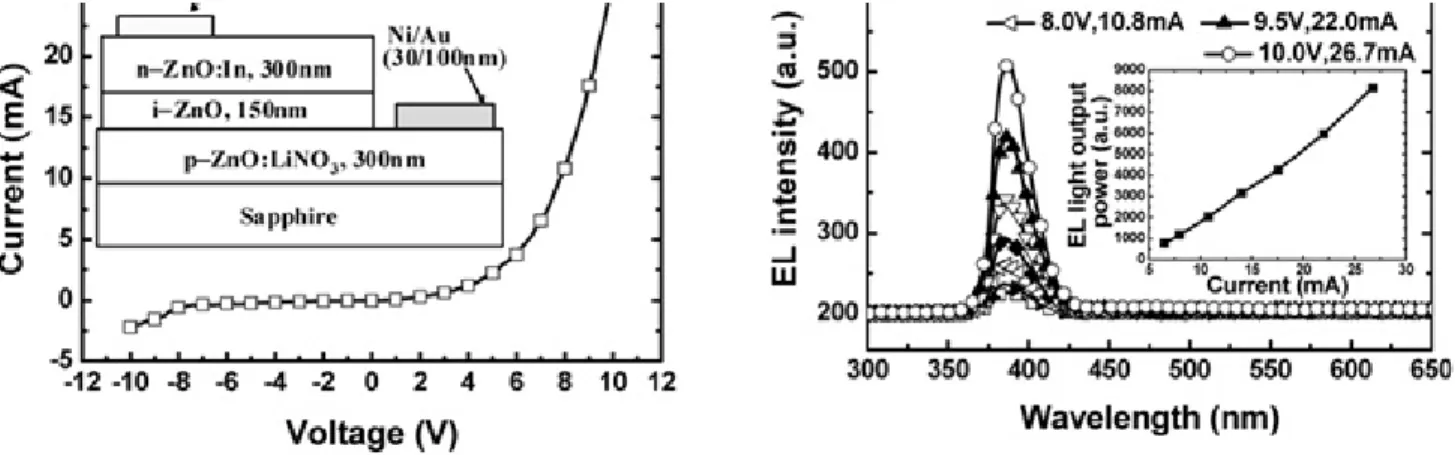
Figure 1 shows the current-voltage characteristics of the pure ZnO-based n-i-p ultraviolet light-emitting diodes. The rectifying diode-like behavior of the ZnO-based n-i-p ultraviolet light-emitting diodes was obviously found in Fig. 1.
The forward turn-on voltage and the reverse breakdown voltage were 3.5 V and -8 V, respectively. Figure 2 shows the electroluminescence spectra of the resulting ZnO-based n-i-p ultraviolet light-emitting diodes measured by a spectrum meter. A single ultraviolet emission at the peak wavelength of 387 nm was found in the electroluminescence spectra.
Since the carrier concentration of the i-ZnO layer is much smaller than that of the p-ZnO:LiNO3layer and the n-ZnO:
In layer, the ultraviolet emission is believably to be the near-band edge (NBE) emission in the i-ZnO layer.
Furthermore, the electroluminescence light output of the NBE emission increased with the injection current as shown in Fig. 2. To integrate the NBE emission band, the total electroluminescence light output power as a function of the injection current is shown in the inset of Fig. 2. Because no green-yellow emission band was observed in the electroluminescence spectra shown in Fig. 2, we could deduced that the defect density existed in the ZnO films was very low enough. The high quality ZnO films of the ZnO-based n-i-p ultraviolet light-emitting diodes could be deposited using the designed vapor cooling condensation system. The low cost vapor cooling condensation system can be expected to be used in the versatile ZnO-based devices in the near future, because high quality n, i, and p-ZnO can be obtained.
1 of 2
Research Express@NCKU - Articles Digest
Fig. 1. Current-voltage characteristics of the ZnO- based n-i-p ultraviolet light-emitting diodes. The inset shows the schematic configuration of the ZnO-based n-i-p ultraviolet light-emitting diodes.
Fig. 2. Room-temperature electroluminescence spectra of the ZnO-based n-i-p ultraviolet light-emitting diodes.
The inset shows the electroluminescence light output power-current characteristics of the ZnO-based n-i-p ultraviolet light-emitting diodes.
2 of 2