國立臺灣大學理學院物理學系 博士論文
Department of Physics College of Science
National Taiwan University Doctoral Dissertation
局域性表面電漿子紅外線奈米光子元件之製作與應用 Preparation and applications of localized surface
plasmon polariton based infrared nanophotonic devices
鄭程文
Cheng-Wen Cheng
指導教授: 施閔雄 博士 陳智泓 博士 Advisors: Min-Hsiung Shih, Ph.D.
Chyh-Hong Chern, Ph. D.
中華民國 101 年六月
June, 2012
致謝
在五年博士研究生涯中,充滿挑戰、挫折、忙碌、充實與成功。其研究成果要 感謝曾經啟發、幫助與支持我的人。以下的文句絕對不足以表達描述我的致謝,
但卻已在我生命的記憶中,留下不可抹去T的足TT跡與色彩T。
首先要感謝我的指導教授施閔雄老師,提供很好的研究環境與自由,並啟發我 做研究的思維與方法。雖然研究過程有遇到挫折,但老師總能適時提供解決問題 建議與想法,讓我能夠順利克服研究困難或避開一些不重要的次要問題。回想到 此,能如其順利畢業與自我的成長,真是心中充滿感謝,感謝老師的栽培。
再者,我要感謝我TIGP同學TMohammedTT
Nadhim
TTAbbas的理論模擬與研究分享,沒有他的幫忙就沒今天的完整研究成果。在博士班期間,我必須感謝研究助理:T
怡君、湘諭與昭瑋幫忙處理行政瑣事和元件量測與製作,以及實驗室同學:功書 和晉源研究上交流討論與光學量測。感謝學弟們:子倉、耀瑩、子庭與坤廷,在 實驗上的大力幫助和許多做實驗熬夜戰鬥夜晚的陪伴。還有謝謝TIGP行政助理 小姐亮慧和物理系辦季先生,學校行政事務的協助與幫忙。
最後,十分感謝與感恩我的家人,爺爺、奶奶、爸爸、媽媽、妹妹對我攻讀博 士的支持,讓我在做研究時無後顧之憂,順利取得博士學位。
感謝曾經幫助我的人,期許在未來的日子自己能夠更精進並有所回饋,祝福大 家一切平安順利。
應用奈米光子實驗室 鄭程文 中華民國一○一年六月
中文摘要
在本論文中,我們利用表面電漿子和局域性表面電漿子的光學獨特性,在理論 和實驗上展示一些主動與被動表面電漿元件,例如窄頻寬熱輻射器、與入射角和 偏振無關紅外線濾波/吸收器、全向性紅外線偏振片和高性能折射率感測器。
根據克希荷夫熱輻射定律,利用金屬圓形碟盤結構,我們製作出一個高效率
紅外線窄頻寬熱輻射器。對於TE 與 TM 入射偏振光而言,此圓形結構具有一個
局域性表面電漿子模態。此模態造成一個無偏振性窄頻寬熱輻射峰,其輻射波長
與頻寬為4.27μm 和 0.25μm. 其窄頻寬、下邊帶、高強度熱輻射特性,可應用在
紅外線熱輻射光源。
關於應用在光學上的濾波/吸收器,我們通常需要高入射角度容忍度。不過,
大多報告過的濾波/吸收器的濾波品質都與入射角度有關。在本文第四章,我們
展示一個 T 型陣列結構製作在銀/二氧化矽/銀基板上,其結構具有一個與入射
角度無關的表面電漿子模態。此結構可做為一個無入射角限制之反射式帶止濾波 /吸收元件,應用在紅外線波段。藉由改變此結構幾何,其濾波頻帶位置可被調
控。無入射角限制的特點,使此 T 型結構濾波元件設計,更加靈活彈性於光學
波導模態共振濾波元件、表面電漿子濾波元件和多層表面電漿結構濾波元件。為 了提升其元件吸收特性和降低製程技術困難,我們提出一個金屬圓形碟盤結構陣
列,並具有一條局域性表面電漿子能帶,其入射角容許值接近達90 度。有別於
之前研究結果,我們實驗與嚴格耦合波理論模擬結果顯示,此局域性表面電漿子 共振波長與圓形碟盤周期無關。利用與周期無關的特性,我們製作出一個大頻寬
的紅外線吸收器,頻寬可到 2000nm。我們又發現調變圓形碟盤與單位晶胞面積
比,一個高性能、廣角、無偏振性的雙波段吸收器可被實現,在寬廣入射角範圍
下,其吸收器最大兩個吸收峰值可超過84%。此結果,可靈活運用在吸收器設計,
特別是在熱光電元件、感測器和偽裝等用途。
除了,金屬圓形碟盤結構陣列在第三與第四章所提的吸收與輻射特性外,我們
發現改變碟盤結構的長短軸比,其TE 和 TM 共振峰可分開。因此,金屬橢圓形
碟盤結構可以濾掉TE 或 TM 反射光,做為一個便宜的全向性紅外線偏振片。在
實驗上,使用碟盤結構長短軸比0.65,發現極化率 99%在波長 4.12μm 為 TE 共
振模態和 91%在 5.25μm 為 TM 共振模態,其實驗結果與模擬一致。TM 與 TE
共振模態消光比各為20dB 和 15dB,藉由調變結構長短軸比,此消光比可進一步
提高。
在最後第六章,我們利用橢圓碟盤陣列在蝕刻二氧化矽層的結構,成功製作出
一個高性能表面電漿子折射率感測器,運作波長範圍從 1000nm 到 1800nm。感
測器的靈敏度和品質因子各為691nm/RIU 和 2.5,此靈敏度和品質因子數值,為
目前為止近紅外線波段最高記錄。在本章中,我們會介紹一個新的概念有效提升 其感測性能。此感測概念,有助維持局域性表面電漿子感測器性能。在將來工作 中,我們與中央研究院應科中心董奕鐘教授合作,將靶細胞放在此元件上,做為 細胞偵測用途。
在附錄 A 和 B,我們將介紹可調變表面電漿子能隙和感應光電壓在金光柵上
的基礎性研究。根據上述 T 型陣列結構,當我們增加在二氧化矽夾層的金屬柱
狀長度,表面電漿子能隙會存在出現。此能隙並非由額外半周期光柵造成,而是 由於金屬-金屬和單層金屬折射率對比造成的。其能隙大小與金屬柱狀長度呈線 性正比。此結構可廣範應用在能隙波導和缺陷共振腔雷射/發射器。
在附錄B,我們與美國 Boise State 大學 Wan Kuang 教授合作,研究在金光柵
上的感應光電壓。我們利用半古典電磁模型和弱非線性近似,來描述金光柵上的 感應光電壓。此模型利用有限元素法來模擬並與量測結果比較。模擬感應光電壓 是入射角和波長的函數,與我們實驗結果符合。此結果,提供一條描述更加詳細,
研究光子-電子交互作用在元件上的路。
Abstract
In the thesis with the unique properties of surface plasmon polaritons (SPPs) and localized surface plasmon polaritons (LSPPs), a number of active and passive surface plasmon-based elements on chips were demonstrated numerically and experimentally, such as a narrow-band thermal emitter, wide-angle polarization independentT infrared filters/absorbers, Tan omni-directional mid-infrared polarizer, and a high-performance index sensor.
Based on the Kirchhoff’s law of thermal radiation with a round-shaped metal disk array, we demonstrated an efficient narrow-band thermal emitter in the MIR region. The structure exhibits one significant LSPP mode for both TM and TE polarizations, leading to an un-polarized narrow emission peak observed at 4.27μm with a FWHM of 0.25μm. This kind of emission property with narrow bandwidth, low sideband and high intensity is very useful for the application in IR light sources.
For the applications in optical filters/absorber, large incident angle tolerance is always in demand. However, most of reported filters/absorbers are angle-dependent.
In chapter 4, we demonstrated a T-shaped array in ARgR/SiOR2R/ARgR platform, showing an angle-independent LSPP mode. The structure can be as an angle-independent reflection-type band-stop filter/absorber in mid-infrared (MIR) region. The stop-band can also be adjusted by varying the structure geometry. The angle-independent feature makes the designed filter more flexible than a guided-mode resonance dielectric filter and a SPP filter as well as a plasmonic multilayer filter. To further improve the absorption performance and reduce the fabrication TdifficultyT, a round-shaped metal disk array is applied because it has a LSPP band over a broad range of incidence angles of up to nearly 90°. Different from the previous work of the round-shaped metal disk array, our experimental results and numerical simulations performed by
using rigorous coupled-wave analysis (RCWA) clearly revealed that the resonant wavelength of the LSPP band is independent of the disk periodicity. Based on the periodic independent result, a broadband absorber with a bandwidth 2000nm operating at MIR region can be realized. We also found that by manipulating the disk area ratios per unit cell (ie area fill factors) and disk sizes, a high-performance, wide-angle, polarization-independent dual band absorber with two maximal absorptivity peaks greater than 84% over a wide of range of incident angles was experimentally achieved. The results demonstrated a substantial flexibility in absorber designs for applications in thermal photovoltaics, sensors, and camouflage.
In addition to the absorption and emission properties of the round-shaped disk structure in chapter 3 and chapter 4, we found that by tuning the aspect ratio b/a of the disk structure, both angle-independent TE- and TM- polarized resonant peaks can be separated. Therefore, the oval-shaped disk based structure can filter out completely one component of the light polarization and reflects perfectly the other component of the light polarization as a cheap omni-directional mid-IR polarizer. In our experiments, we found that such structure with b/a=0.65 (a=1543nm, b=1009nm) has a degree of polarization 91% at wavelength 4.12μm for TE mode and 99% at 5.25μm for TM mode, showing a good agreement with our simulation. The extinction ratios for both TM and TE modes are 20dB and 15dB, all of which can be further improved by tailoring the b/a axial ratio.
In the last chapter 6, based on the oval-shaped disk array structure with the SiOR2R
layer etching, a highly performance plsmonic index sensor operating at wavelengths from 1000nm to 1800nm can be realized. The sensitivity 691nm/RIU and FOM=2.5 can be achieved as the highest record up to now in the NIR region. In the chapter, we also introduce a novel concept for the improvement in plasmonic sensing. The sensing strategy based on the concept can offer great potential to maintain the performance of
LSPP sensors. In the future work, we will cooperate with Professor Yi-Chung Tung at RCAS, Academic Sinica to produce target cells on such device for the cell detection.
In Appendix A and B, fundamental studies of a tunable SPP band gap and photon induced voltage on an Au grating slab are introduced, respectively. Based on the T-shaped structure with the post under the top grating, a SPP band gap in Appendix A, can occur without using extra periodic grating ΛRgR/2 when the post length is increased. The SPP band gap is attributed to the index contract between the metal-metal and single metal regions, and is linearly proportional to the post length.
Such a T-shaped structure with a tunable LSPP band gap can be widely exploited in various applications, such as band gap waveguides and defect cavity lasers/emitters.
In Appendix B, we cooperated with professor Wan Kuang’s group at Boise State University, USA to study photon induced voltage on an Au grating slab. A semi-classical electrodynamic model is developed for the Au grating slab under the weak nonlinearity approximation. The model was solved by finite element method and compared with our measurements. The calculated photon induced voltage as a function of incident angles and wavelengths was found to be in qualitatively agreement with the experimental measurements, giving a pathway for the study of devices with more detailed photon electron interactions.
Contents
Chapter 1 Introduction and motivation……….……..………1
Chapter 2 Fundamentals of surface plasmon polaritons (SPPs) and localized surface plasmon polaritons (LSPPs)....6
2.1 Basic principle of surface plasmon polaritons…6 2.1.1 SPPs at a single dielectric/metal interface...6
2.1.2 SPPs at a dielectric/metal/dielectric double interface...14
2.1.3 SPPs at a metal/dielectric/metal double interface...18
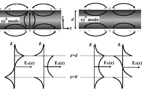
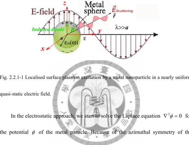
2.2 Basic principle of localized surface plasmon polaritons………..… 20
2.2.1 LSPPs at a sub-wavelength metal particle...20
2.2.2 LSPPs at a metal/dielectric/metal cavity...25
Chapter 3 Angle and polarization independent narrow-band thermal emitter made of metallic disk on SiO
R2R……….30
3.1 Design and simulation... 31
3.2 Experimental setup and results...33
3.3 Summary...
37
Chapter 4 Wide-angle plasmonic infrared filters/absorber.38 4.1 Design and simulation of the Ag/SiO
R2R/Ag T-shaped array ... 39
4.2 Fabrication of the Ag/SiO
R2R/Ag T-shaped array...42
4.3 FTIR measurement setup... 44
4.4 Experimental results of the Ag/SiO
R2R/Ag T-shaped array... 45
4.5 Design and simulation of the 2D metal disk array absorbers...48
4.6 Fabrication of the 2D metal disk array absorbers...42
4.7 Experimental results of the 2D metal disk arrays...51
4.8 Summary... 57
Chapter 5 Omni-directional mid-infrared (MIR) polarizer
made of elliptical metal disk arrays.……….. 59
5.1 Design and simulation...
60
5.2 Fabrication of the MIR polarizer...63
5.3 Experimental results and discussion...
64
5.4 Summary...
69
Chapter 6 Plasmonic index sensor made of elliptical metal disk array………..70
6.1 Design and simulation...
71
6.2 Fabrication of the Au/SiO2 cavity based structure... 74
6.3 Experimental results and discussion...
75
6.4 Summary and future work...
78
Chapter 7 Conclusion………..…
80
Appendix A……….………..…
83
Appendix B……….………..…
96
Appendix C……….………106
Bibliography………...
108
List of Figures
Fig. 1-1. Lycurgus cup is a Roman glass cup stored Tin the Bristish Museum...1 Fig. 2.1.1-1 Surface plasmons at interface between a metal and a dielectric material have a combined electromagnetic wave and surface charge distributionT...7 Fig. 2.1.1-2 Schematic diagram of TM-polarized fields in two media and1 when 2 surface plasmon mode is excited by a polarized incident filed. The surface charge density wave (or surface plasmon wave (SPW)) will propagate on a metal surface in the x direction...….8 Fig. 2.1.1-3 Dispersion relation of radiative and non-radiative surface plasmon modes where the dotted line is an asymptote of the blue curve for the radiative surface plasmon mode………..12 Fig. 2.1.1-4 Configuration of the ATR method where the evanescent field generated from the prism couples with the SPPs on the interface between and2 if 1
completely matches
k
xk ………...13
SPFig. 2.1.1-5 By tuning the angle of incidence to the prism base in the ATR method, the SPPs at dielectric/metal interface can be excited when
k
x k
SP………..13 Fig. 2.1.2-1 Schematic diagram of TM-polarized fields in three media
1,
2, and
3. The metal thin film
2 lies between dielectric
1and
3. Whincoming TM-polarized field, surface plasmon waves (SPW) will propagate on both sides of the thin film surfaces………...14 Fig. 2.1.2-2 Distribution of fields for both high- and low- frequency modes in a symmetric plane of a metal thin film………18 Fig. 2.2.1-1 Localised surface plasmon excitation by a metal nanoparticle in a nearly uniform quasi-static electric field……….21 Fig. 2.2.2-1 Lowest-order TM mode of metal/dielectric/metal (a) open and (b) closed cavities with a length of L………26
en SPs are excited by an
Fig. 2.2.2-2 Schematic diagram of the investigated MD structure…...27 Fig. 2.2.2-3(a) TM- and (b) TE-mode stimulated reflectance spectra of the MD structure...29
r normal incidence in (a) X-Y plane at Z=40 nm and (b) X-Z plane at Y=0
iameters D for θ=0° when t=50nm. The inset shows resonance wavelength (λ) versus
ig. 3.2-1(a) Side view of thermal emitter chamber... 34 ig. 3.2-1(b) Top view of thermal emitter chamber...34 ig. 3.2-2(a) Measured reflectance spectra of sample with D=1.15μm and Λ=3μm... 35 ig. 3.2-2(b) Simulated and measured emission spectrum of the IR emitter at 220 °C
ig. 3.2-2(c) The measured emission spectrum for unpolarized, s-polarized
ig. 4.1-1(a) Illustration of the T-shaped array structure. (b) Illustration of the
ig. 4.1-2(a) Stimulated reflectance spectra in x-z plane. (b) Stimulated reflectance
ig. 4.1-2(c) |HRyR|P2P distribution at 0.35ev in x-z plane...
Fig. 2.2.2-4 TM-polarized |HRyR|P2P distributions in one pitch of the MD array at 0.35 eV fo
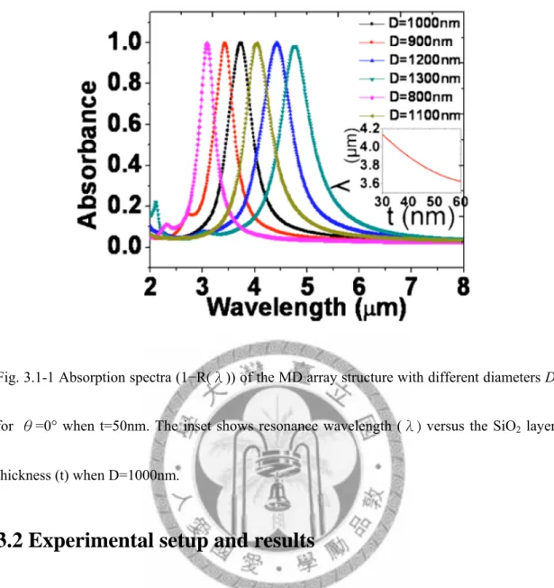
nm...29 Fig. 3.1-1 Absorption spectra (1−R(λ)) of the MD array structure with different d
the SiOR2R layer thickness (t) when D=1000nm...
33 F F F F
(blue line) and 300 °C (black line), respectively...36 F
(TE-polarized) and p-polarized (TM-polarized) for 220 °C... 36 F
reflection-type filter with the designed structure... 39 F
spectra in y-z plane...41 F
42
Fig. 4.2-1 Fabrication process of the T-shaped array...42
Fig. 4.2-2(a) 45° angle SEM image of the T-shaped array. (b) Cross-sectional SEM image of the T-shaped structure... 43 Fig. 4.3-1 Experimental setup for measurements………...…..44 Fig. 4.4-1 (a) Incident (green), reflectance (red), and absorbance (blue) spectra at normal incidence. (b) Normal incident absorbance spectra from the T-shaped arrays with the widths WRAgR =300 nm, 1540 nm, and 1910 nm. (c) Comparison of calculated and measured wavelengths of resonance………..46 Fig. 4.4-2 Absorbance spectra from the T-shaped array with incident angles in x-z plane from 0° to 15°. The accuracy of the measured spectra is 3 nm………..47 Fig. 4.6-1 SEM image of a fabricated MD structure…...50 Fig. 4.7-1(a) Comparison of the calculated and measured wavelengths of resonances as functions of the disk diameter D... 51 Fig. 4.7-1(b) Absorptivities at normal incidence of the 1 μm MD arrays with several different periodicities Λ... 53 Fig. 4.7-1(c) Absorptivities of the MD arrays with different diameters D for Λ fixed at 3 μm...53 Fig. 4.7-1(d) Experimental peak absorptivity of the MD configuration as a function of its area-fill factor F... 54 Fig. 4.7-2(a) Experimental absorptivity of the broadband absorber composed of the multi-sized disks with D=800 nm, 900 nm, 1.03 μm, 1.12 μm, 1.21 μm, and 1.35 μm and a SiOR2R spacer thickness, tRSiO2R=32 nm...
55
m...56
Fig. 5.1-1 Illustration of the metallic disk array structure...60 Fig. 4.7-2(b) Absorptivity of the dual-band absorber consisting of two different disk sizes with dimensions D=820 nm, and 920 nm per unit cell when tRSiO2R=80 n
Fig. 5.1-2 Dispersion relation of the metal disk structure for (a) TM mode and TE
mode... 61
eld distribution for TE-mode at 0.37eV in X-Z plane... 62
ig. 5.1-4 Calculated extinction ratio versus axial ratio... 63
ig. 5.2-1 SEM image of an elliptical disk array………...64
iangles and circles, respectively...66
urves... 66
ig. 5.3-2 Absorbance spectra at different incident angles from 0PoP to 15PoP... 68
511nm when a is fixed approximately 1511nm...68
ig. 6.1-1 Illustration of the Au/SiOR2R/Au cavity based structure... ig. 6.1-2 |HRyR|P2P distribution of the (a) round-shaped metal disk and (b) oval-shaped ig. 6.1-3 (a) Illustration of the oval-shaped Au/SiOR2R disk structure. (b) |HRyR|P2P Fig. 5.1-3(a) |HRyR|P2P field distribution for TM-mode at 0.33eV in X-Z plane. (b) |HRxR|P2P fi F F Fig. 5.3-1(a) Measured reflectance spectra of the proposed metal disk structure for TM-polarized light (red), TE-polarized light (blue), and un-polarized light (green). The corresponding simulated spectra for TM- and TE- polarized light are shown in tr Fig. 5.3-1(b) Polar diagram of the reflectance spectra versus polarizer rotating angle where the TE- and TM- polarizations of light by reflection are shown in red and blue c F Fig. 5.3-3 Measured absorbance spectra for different minor axes from 585nm to 1 F 71 F disk structures within one unit cell at the Y-Z plane when X=0... 72
F distribution within one unit cell at the Y-Z plane when X=0……... 72
Fig. 6.1-4 Numerical simulations of the sensitivities for the three structures... 74 Fig. 6.2-1 SEM view of the oval-shaped Au/SiOR2R disk structure...
75
Fig. 6.3-1 Measured absorbance spectra of the three cavity based structures with liquid Tindices from 1 to 1.39T...
77
ig. A-2 (a) Stimulated reflectance spectra of the multilayer structure with design
5
ultilayer structure at the crossing point 0.87 eV, and (b) the first and (c) second
xed at 200 nm. (b) Energy gap versus WRpostR when the tRpostR =170 nm……….
iew of the T-shaped array with a displacement of d=50 nm. The inset shows the
cidence under TE-, TM-, and un-polarized illumination……….. 91
RtopR =570 nm, tRtopR=200 nm, WRpostR=200 nm, tRpostR=0 nm, and Gt=320 nm) and (b) the
nd (b), the simulated absorbance spectra are represented by black solid curves……93 Fig. 6.3-2 Peak wavelength shifts in the TM-modes of the three structures... 78 Fig. A-1 Schematic diagram of the T-shaped array structure………..………..84
F
parameters of ΛRgR=1 μm, WRtopR =550 nm, tRtopR=200 nm, WRpostR=200 nm, d=0 nm, tRpostR=0 nm, and GRtR=320 nm. (b) Stimulated reflectance spectra of the T-shaped structure when d=50 nm, tRpostR=170 nm, and GRtR=150 nm………...………..
8
Fig A-3 |HRyR|P2P distribution at normal incidence in one period of (a) the Ag/SiOR2R/Ag m
branches of the T-shaped structure when d=50 nm, tRpostR=170 nm, and GRtR=150 nm….
86
Fig. A-4 (a) Energy gap of the T-shaped structure varying with tRpost Rwhen the WRpostR is fi
88
Fig. A-5 (a) The fabrication process of the T-shaped Ag/SiOR2R/Ag structure. (b) SEM v
details of the structure with a tilt angle of 25° at the ends of the grating slabs on the Ag posts. (c) AFM image profile of the T-shaped grating………..……. 89 Fig. A-6 Experimental absorbance spectra of the T-shaped grating (ΛRgR=1 μm, WRtopR
=620 nm, tRtopR=200 nm, WRpostR=200 nm, tRpostR=170 nm, and Gt=150 nm) at normal in
Fig. A-7 Experimental absorbance spectra of (a) the multilayer structure (ΛRgR=1 μm, W
T-shaped structure (ΛRgR=1 μm, WRtopR =620 nm, tRtopR=200 nm, WRpostR=200 nm, tRpostR=170 nm, and Gt=150 nm) for the different incident angles θRiR = 0°, 5°, and 10°. In both (a) a
Fig. A-8 1D photonic dispersion curve of the slab with the constituent dielectrics 1=1.414 and n2=2.236, when ΛRgR=1 μm, tRSiO2R=320 nm, and WRpostR=200 nm……...
ig. B-1 Photon induced current density as calculated by the hydrodynamic model
ig. B-2 SEM image of an Au grating. The inset shows the details of the grating....102
ig. B-3 Induced voltage peaks as a function of incident angle for incident avelengths of 1.2, 1.3, and 1.4μm………104 ig. B-4 Measured photon induced voltage as a function of incident angle and
avelength………... 104 n
94 F
where the white open circles indicate the position of peak response...100 F
F w F w
Chapter 1 Introduction and motivation
Surface plasmons (SPs) are quantized collective charge oscillations that occur at the interface between metal and dielectric. When SPs are coupled with photons, it can take various forms, ranging from freely propagating electron density wave along the interface (also called surface plasmon polaritons SPPs) to localized electron oscillations on the metal surface (also referred as localized surface plasmon polaritons LSPPs). The surface plasmon coupling effect has been employed for a long time by artists to generate vibrant colors in glass artefacts and in the staining of church windows. One of famous example is the Lycurgus cup (see Figure 1-1) dating from the 4th century A. D.
Fig. 1-1. Lycurgus cup is a Roman glass cup stored in the Bristish Museum.
The glass cup shows a striking red when transmitted light is emitted from a light source placed inside the cup, while appearing green in reflection when light source is removed from the cup. This color change behavior is because of localized plasmonic
excitation of metallic particles in the glass matrix, leading to a bit change in the extinction (
C ), scattering (
extC ), and absorption (
scaC ) cross sections of the
abs metallic particles.Some of the first scientific research in surface plasmons was observed at the beginning of the 20 century. In the year 1902, extraordinary phenomenon in optical reflection measurements on metallic gratings were first observed by Robert W. Wood [1]. In 1904, bright colors found in metal-doped glasses was described by Maxwell Garnett using the Durde theory of metals [2], and the electromagnetic properties of small spheres [3] were derived by Lord Rayleigh (J. W. Strutt) who won the Nobel Prize in physics in this year. Four years later, the theory of light scattering by spherical particles (particle size is about the same size as wavelength of incident light), which is well known as Mie theory [4], was developed by Gustav Mie. After some 50 years, in 1956, David Pines theoretically described the energy losses from electrons traveling through metals [5], corresponding to the collective oscillations of free electrons in the metal. He called such oscillations ‘plasmons’. In 1957, Rufus Ritchie found that plamons can exist near the surface of metals when electron energy losses occur [6]. A major advance in the study of surface plasmon ploaritons was in 1968 (nearly 70 years after Wood’s original observations) when Andreas Otto [7] and Erich Kretschman as well as Heinz Reather [8] developed a method called attenuated total
reflection (ATR). The method makes the excitation of surface plasmon polritons easier and is accessible to many fields of research. In terms of the optical properties of localized surface plasmon polaritons, in 1970, Uwe Kreibig and Peter Zacharias first described the optical properties of gold and silver nanoparticles [9]. As the field, sometimes called plasmonics, continuingly developing, the coupling effect between the oscillating electrons and the electromagnetic field become more interesting and important in many applications.
The recent surge in surface plasmon-based applications is mostly focused on the research areas such as optical lithography, optical data storage, and high density photonic integrated circuits. The design and manufacturing in the research areas are all approaching fundamental physical limits. Such challenges could be overcome by using the properties of surface plasmons. Owing to many recent studies, a wide range of surface plasmon-based applications and techniques are developed, such as light guiding and manipulation at nanoscale [10, 11], surface-enhanced Raman scattering (SERS) from molecules adsorbed on small metal particles [12], single molecule biodetection [13, 14], optical transmission enhancement via sub-wavelength apertures [15], high resolution imaging below the diffraction limit [16], and so on.
In terms of communication systems, nm-sized electronic (metallic) circuits are inherently slow due to resistor-capacitor (RC) delay time limiting its
data-transmission speed, whereas optical (dielectric) circuits having high data-transmission speed are μm-sized due to optical diffraction limit. However, it is fascinating to note that surface plasmon-based photonic circuits can combine the compactness of the electronic circuits with the broad bandwidth of the optical circuits.
By employing the unique property of SPPs, most attractive surface plasmon components are mainly designed for reflectors [17], resonators [18, 19], and subwavelength waveguides [10, 20-22] with the guiding and confinement properties of electromagnetic radiation in light. In additional to the SPPs, the non-propagating LSPP property offers a potential in many applications such as filters [20, 21], metamaterial coatings [22], sensors [14, 23-32], solar cells [23-26], spasers [27], thermal emitters [28-31], and thermalphotovoltaic (TPV) converters [32, 33]. Using those plasmonic properties, a number of active and passive surface plasmon-based elements have been developed, bringing the dream of a surface plasmon-based photonic integrated circuit into reality. A surface plasmon-based photonic integrated circuit includes a range of elements on a chip such as waveguides, modulators, filters, detectors, emitters and lasers. In the thesis with the unique properties of LSPPs, a narrow-band emitter [31], wide-angle plasmonic filter [21]/absorbers [34], an omni-directional mid-infrared polarizer, and a high-performance index sensor will be introduced and demonstrated.
The thesis content is organized as follows: in chapter 2, the basic theoretical background on SPPs at single and double interfaces and LSPPs on metal nanoparticles and metal/dielectric/metal cavities are looked at. Later on, we will develop and characterize a narrow-band thermal emitter in chapter 3, angle-independent filters/absorbers in chapter 4, a mid-infrared polarizer with an ultrahigh immunity to incident angles in chapter 5, and a high-performance plasmonic sensor in chapter 6.
Finally, in chapter 7, we conclude the results and offer some suggestions for those localized surface plasmon-based devices.
Chapter 2 Fundamentals of surface plasmon polaritons (SPPs) and localized surface plasmon polaritons (LSPPs)
In the chapter, surface plasmon polaritons (SPPs) at a single dielectric/metal interface, the SPP propagation and decay lengths, and the condition of SPP excitation are introduced. In additional to the properties of the SPPs, SPP multiple-interface systems including dielectric/metal/dielectric (DMD) and metal/dielectric/metal (MDM) heteostructures are also looked at. As to localized surface plasmon polaritons (LSPPs), the LSPP properties of a sub-wavelength metal particle and MDM resonant cavities will be discussed.
2.1 Basic principle of surface plasmon polaritons
2.1.1 SPPs at a single dielectric/metal interface
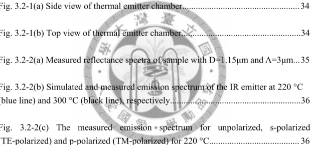
Surface plasmon polaritons (SPPs) are electromagnetic waves coupled to the surface charge oscillations of a metal surface. The electron charges on the metal surface can perform coherent electron oscillations propagating along the surface (ie surface plasmon wave) as shown in Fig. 2.1.1-1. The surface charge distribution is described by
)]
( exp[
)
(x O i kxx t
(2.1.1-1)
where
O is a constant for the surface charge density on the surface, and kx is awave vector of the surface wave. At the surface boundary, a condition
4 ) ( 2 1
D D
z
must be satisfied where
z
is a normal directed from side 1 to 2,and
D
idisplacements are
D
i iE
i
with dielectric constants
i produced by boundcharges, not free charges. Thus, from the surface condition formula, it can be understood that SPPs only occur in the field with TM modes (p-polarization), the modes on the plane of incidence allowing the existence of a normal component of electric field Ez.
Fig. 2.1.1-1 Surface plasmons at interface between a metal and a dielectric material have a
combined electromagnetic wave and surface charge distribution.(Adapted from [35])
Assuming there is an interface between a dielectric medium ( =1,2 ) and a 2 metallic layer (
1=1,
1) where dielectric constants
i (i1,2)are more generally allowed to be complex including bound charge and free charge contributions. When SPPs occur, the TM-polarized fields with a sinusoidal time dependence termt
e
i propagating through the layer system as seen in Fig. 2.1.1-2 are as follows:) (
exp ) 0 , , 0
( 2 2 2
2
H i k x k z t
H
y x z
(2.1.1-2) )
( exp ) , 0 ,
( 2 2 2 2
2
E E i k x k z t
E
x z x z
(2.1.1-3) )
( exp ) 0 , , 0
( 1 1 1
1
H i k x k z t
H
y x z
(2.1.1-4) )
( exp ) , 0 ,
( 1 1 1 1
1
E E i k x k z t
E
x z x z
(2.1.1-5) where z>0 for
H
2and
E
2, z<0 for
H
1and
E
1, and x for all fields.
Fig. 2.1.1-2 Schematic diagram of TM-polarized fields in two media
1and
2 when surface plasmon mode is excited by a polarized incident filed. The surface charge density wave (orsurface plasmon wave (SPW)) will propagate on a metal surface in the x direction.
These fields above at z>0 and z<0 fulfil the following Maxwell’s equations:
0
i
E
i
and iH
it
E
c
1
i=1,and 2 (2.1.1-6)
0
H
iand i i
E
it
H
c
1 i=1,and 2 (2.1.1-7) From the Maxwell’s equations, the boundary conditions at z=0 are given byx
x
E
E
2 1 ,H
2y H
1y, and
2E2z
1E1z (2.1.1-8) In addition, the existence of the boundary conditions at z=0 must be satisfied at all points on the plane at all time, which means the spatial and time variation of all fields must be the same. Consequently, the phase factors at z=0 we require are [36]0 1
0
2 )| ( )|
(
k
r
z k
r
z(2.1.1-9) By the phase factor requirement at z=0,
k
2and
k
1would be located on the same plane of incidence with
k
2x k
1x k
x andk
2y k
1y 0. Withk
2x k
1x k
x, the boundary conditionH
2y H
1y and (2.1.1-7) into which (2.1.1-2) to (2.1.1-5) substitute, we can obtain the following simultaneous linear equations in 2 unknowns:0 0
2 2 2 1
1 1
2 1
y z y z
y y
H k H k
H H
(2.1.1-10)
To obtain non-trivial solution of the simultaneous equations (ie
H
1yandH
2y are non-zero), the determinant det(A) of the equations must be zero, where0 1
1 ) det(
2 2 1 1 2 2 1
1
z z z
z
k k k
A k
(2.1.1-11)and 2 2
2
2z i( ) x
i
k
k
c
i=1, and2.From equation (2.1.1-11) together with 2 2
2
2z i( ) x
i
k
k
c
i=1, and 2, the well-known dispersion relation for the case of interface SPPs is obtained:) (
2 1
2 1
kx c (2.1.1-12)
In general,
k
x(
)can be complex. If we assume
1
1' i
1'' and
1''
1' , )(
k
x =k
x' ik
x'' can be obtained with)
( '
1 2
' 1 ' 2
k
xc
(2.1.1-13)2 ' 1
"
2 1 / 3 ' 1 2
' 1 '' 2
) ( ) 2
(
k
xc
(2.1.1-14) wherek determines the wave propagation of surface plasmons, and
x'k is related to
x'' internal absorption produced by
1".The propagating SPP wave will be damped with an energy attenuation length L (also called propagation length) defined as ''
2 1
k
xL
. As can be seen, when the metalloss associated with
1" is increased, L tends to be decreased. Regarding the penetration depth (also called skin depth) of the SPP wave, the depth is defined asthe SPP field along z-axis falling off exponentially with a value of
e .
1 is therefore given by) ( 1 )
Im(
1
2 2 2
k c k
i x z
i
. For a dielectric/metal interface,
1' 0and 2 0 (|
2 ||
1' |) which in turn results 2 1. The relation between thecomplex refractive index
n
~ n
ik
and permittivity
' i
'' is given by
2
n
~ where μ=1. This explicitly yields2 2 '
n
k
and
'' 2nk
(2.1.1-15) To further simplify the dispersion relationk
x(
)in (2.1.1-12), if we just concernkx real with (pure dielectric medium) and2 1 1 22
p where
p called plasmafrequency ( produced by Drude model for a simple metallic medium), then 1
SP x
x
k k
k
(
) ' can be written as) 1 (
) 1 (
2 2 2
2 2 2
p p x
SP
k c
k
(2.1.1-16)
As
k
x , there is a horizontal asymptote2 1
p . Further from (2.1.1-16),
2 2
2
2z i( ) x
i
k
k
c
becomes) 1 (
) 1 (
2 2 2
2 2 2
1
p p
z
c
k
(2.1.1-17)
) 1
( 2
2 2
2 2 2
p
z c
k
(2.1.1-18)
when
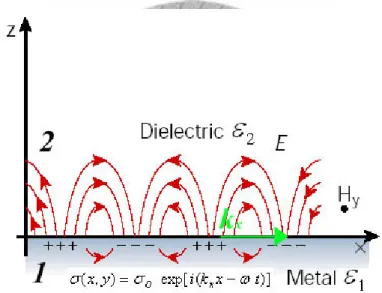
2 1
p (ie (1 2) 0)2
2
p , the SPP wave is also called “nonradiative”surface plasmon polaritons because both k1z and k2z from (2.1.1-17) and (2.1.1-18) are imaginary, leading to exponentially radiation decay near the surface boundary. In
contrast, when
2 1
p , it is called “radiative” surface plasmon polaritons.When
p, the permittivity
1of metal becomes
1 0. If the SPPs exists withk
x in (2.1-11) required to bek
x 0,
1
2 0 and (
1
2)0 must be satisfied.The dispersion relation from (2.1.1-16) can be sketched as seen in Fig. 2.1.1-3. It can be seen that the wave vector kSP of nonradiative surface plasmons is larger than
that of an incident light with an angle
o. Therefore, nonradiative SPPs will not happen naturally when light strikes on a metallic surface.Fig. 2.1.1-3 Dispersion relation of radiative and non-radiative surface plasmon modes where
the dotted line is an asymptote of the blue curve for the radiative surface plasmon mode.
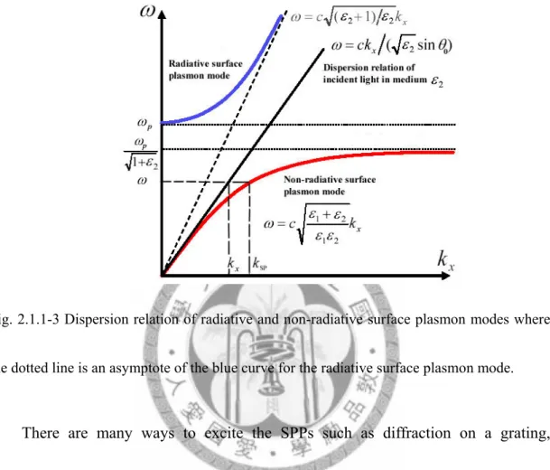
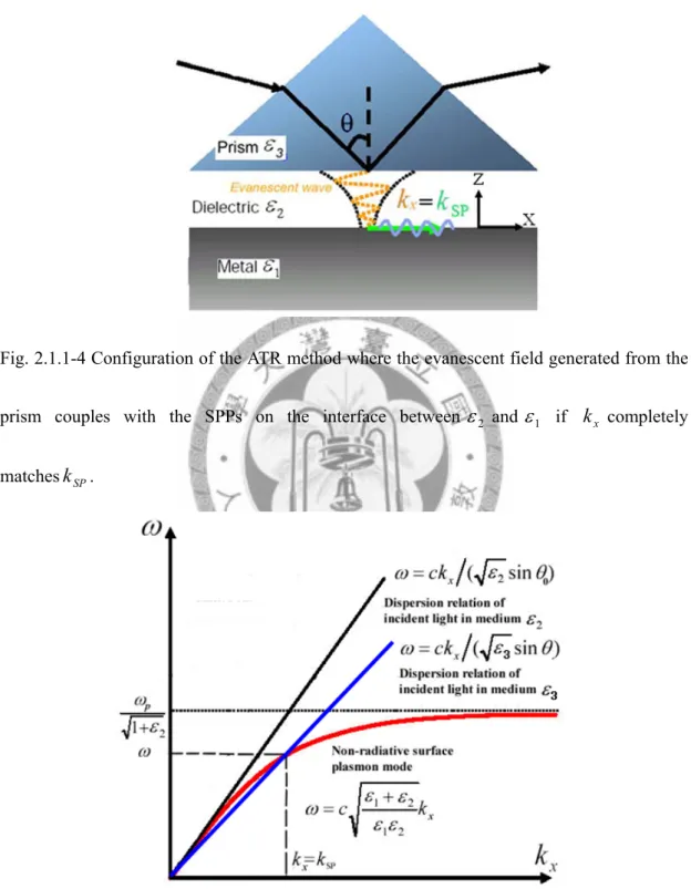
There are many ways to excite the SPPs such as diffraction on a grating, diffraction on surface features, excitation with an SNOM (scanning near-field optical microscopy) probe, and excitation with a prism [37]. One of common ways is to use attenuated total reflection (ATR) coupler to excite SPPs. As to the configuration of the ATR coupler shown in Fig. 2.1.1-4, a prim with
3 is utilised to generate an
2 evanescent light wave withk
x
3(
/c
)sin
where
c(critical angle). By adjusting
into a proper angle, the wave vectork from the prim would completely
x match the SPPs of wave vectork shown in Fig.2.1.1-5, which in turn result in the
SPexcitation of SPPs.
Fig. 2.1.1-4 Configuration of the ATR method where the evanescent field generated from the
prism couples with the SPPs on the interface between
2 and
1 ifk
x completely matchesk
SP.Fig. 2.1.1-5 By tuning the angle of incidence to the prism base in the ATR method, the SPPs at dielectric/metal interface can be excited when
k
x k
SP.2.1.2 SPPs at a dielectric/metal/ dielectric double interface
Up to now we have treated the physics of SPP propagating on a smooth interace of dielectric/metal. SPPs also exist on thin films. Their properties depend on the thickness of the thin film system and the dielectric medium on both sides of the thin film. For the case of SPPs on the thin films, let us first concern a thin film system with a thickness d as displayed in Fig. 2.1.2-1. The metallic thin film between asymmetric dielectrics
1and
2allows the excitation of SPPs by irradiation with TM-polarized light.Fig. 2.1.2-1 Schematic diagram of TM-polarized fields in three media
1,
2, and
3. The metal thin film
2 lies between dielectric
1and
3. When SPs are excited by an incoming TM-polarized field, surface plasmon waves (SPW) will propagate on both sides of the thinfilm surfaces.
The TM-polarized fields in the thin film layer system are given by
in zone 1 where z<0,
) (
exp ) 0 , , 0
( 1 1 1
1
H i k x k z t
H
y x z
(2.1.2-1)
) (
exp ) , 0 , ( ) (
) (
exp ) , 0 , (
1 1
1 1 1 1
1 1
1 1 1
t z k x k i k
H k c
t z k x k i E
E E
z x x
z y
z x
z x
(2.1.2-2)
in zone 2 where 0<d<z,
) (
exp )]
( exp ) 0 , , 0 ( ) ( exp ) 0 , , 0
[( 2 2 2 2 2
2
H i k H i k i k x t
H
y z y z x
(2.1.2-3)
(2.1.2-4)
in zone 3 where z<d,
) (
exp ) 0 , , 0
( 3 3 3
3
H i k x k z t
H
y x z
(2.1.2-5)
) (
exp ) , 0 , ( ) (
) (
exp ) , 0 , (
3 3
3 3 3 1
3 3
3 3 3
t z k x k i k
H k c
t z k x k i E
E E
z x
x z y
z x
z x
(2.1.2-6)
where
E
iand
H
i(i=1,2,and 3) satisfy the equation (2.1.1-7).
With the phase factor requirement mentioned in (2.1.1-9) at z=0, and z=d, the wave vectors of the fields at different zones have following relations:
x x x
x
k k k
k
1 2 3 andk
1y k
2y k
3y 0 (2.1.2-7) By (2.1.2-7) with the boundary conditions where the tangential components ofE
i) (
exp )]
( exp ) , 0 , ( )
( exp ) , 0 , ( 1 [ ) (
) (
exp )]
( exp ) , 0 , ( ) ( exp ) , 0 , [(
2 2
2 2 2 2 2
2 2 2
2 2
2 2 2
2 2 1
t x k i k
i k
k H k i k
k c H
t x k i k
i E
E k
i E
E E
x z
x z y z
x z y
x z
z x z
z x
and
H
i(i=1,2,and 3) are continuous at z=0 and z=d, we therefore obtain:
at z=0,
H1y H2y H2y (2.1.2-8) 2
2 2 2 2 1 2
1
1 ( ) k H
k H
k H z z
z y
(2.1.2-9) at z=d,H2yexpi(k2zd)H2yexpi(k2zd)H3yexpi(k3zd) (2.1.2-10) )
( exp )
( exp )
(
exp 3 3
3 3 2
2 2 2 2
2 2
2 k H i k d
d k i k H
d k i k H
z y
z z
y z z
y z
(2.1.2-11)
where (2.1.2-8) and (2.1.2-10) are for the tangential components of
H
icontinuous at z=0 and z=d. As to (2.1.2-9) and (2.1.2-11), they have tangential components of
E
i continuous at z=0 and z=d. These four equations above from (2.1.2-8) to (2.1.2-11) can be rearranged to be0 ) (
)
( 2 1 1 2 2 2 1 1 2
2y k z k z Hy kz k z
H
(2.1.2-12) 0) ( exp ) (
) )(
(
exp 2 2 3 3 2 2 2 3 3 2 2
2 i k d k k H k k i k d
H y z
z
z y
z
z z (2.1.2-13)If H2yandH2y are required not to be zero, then the following relation in (2.1.2-14) must be satisfied.
) 0 (
exp ) (
) ( exp ) (
) (
) _ (
2 2
3 3 2 2
3 2 2 3
2 1 1 2 2
1 1
2
d k i k
k d
k i k
k
k k
k k
z z
z z
z z
z z
z z
(2.1.2-14)If the metallic thin film is between symmetric dielectrics (ie
1
3
1), (2.1.2-4) can be simply rearranged and split into two following independent equations.0 2 ) tan( 2
2 1 1
2
k d
k i
kz z z
(2.1.2-15)