數位系統設計
Digital System Design
Instructor: Kuan Jen Lin (林寬仁) E-Mail: [email protected]
Web: http://vlsi.ee.fju.edu.tw/teacher/kjlin/kjlin.htm
電子電機產業
半導體 產業
IC 、元件、感測元件
PCB、System board
作業系統、開發工具、驅動程式
消費性、通訊、控制、生醫、多媒體、綠能、
職能類型
軟體工程師 韌體工程師
數位硬體工程師 (IC、系統)
類比硬體工程師 (IC、系統)
數位系統設計相關課程
邏輯設計 (大一下)
可程式系統晶片設計實習(大三下) 邏輯設計實驗
(大二上)
數位系統設計 (Verilog HDL,大二上)
微算機概論(大三上)
Textbook
Main textbook
1. Michael D. Ciletti, “Advanced Digital Design with the Verilog HDL,” Prentice Hall, 2003
References
1. Samir Palnitkar, “Verilog HDL– A Guide to Gidital Design and Synthesis”, Prentice Hall.
2. Thomas & Moorby’s, “The Verilog Hardware Description Language,” 5th edition, KAP, 2002.
Contents
Verilog HDL
Logic design with behavioral models
Synthesis of combinational and sequential logic
Design and Synthesis of Datapath controller
Data path Controller
Grading
期中考 30%
期末考 40%
作業、其他 30%
曠課一次扣總分 10 分,滿 3 次即不及格
遲到一次扣總分 3 分,病假需有醫師之診斷證
明
Design Flow
Specification RTL design and
Simulation Logic Synthesis
Gate Level Simulation
ASIC Layout FPGA Implementation
RTL-level design gate-level design (cell-based)
Transistor-level design
Physical design (layout)
System-level design
邏輯設計、數位系統設計、
可程式系統晶片實習、
數位晶片設計概論(含實
驗) 、
VLSI 電路設計導論、電子學
數位積體電路設計、類比機體電 路設計
微算機、系統晶片設計實驗
Review of Logic Design
Boolean Algebra
Boolean Algebra
A set of elements B and two binary operators + and
‧
1. Closure w.r.t. the operator + (‧)
x, y ∈ B ∋ x+y ∈B
2. An identity element w.r.t. + (‧)
0+x = x+0 = x
1‧x = x‧1= x
3. Commutative w.r.t. + (‧)
x+y = y+x
x‧y = y‧x
Boolean Algebra
4. ‧ is distributive over +:
x‧(y+z)=(x‧y)+(x‧z) + is distributive over‧: x+(y‧z)=(x+y)‧(x+z)
5. ∀ x ∈ B, ∃ x' ∈ B (complement of x)
∋ x+x'=1 and x‧x'=0
6. ∃ at least two elements x, y ∈ B ∋ x ≠ y What are the differences from general
Boolean Cube
Boolean Function
Algebraic Simplification
Multiplying out and factoring
a(b+c) = ab+ac
Combining terms
abc’d+abcd = abd
Eliminating terms
ab+abd = ab
Eliminating literals
a+a’b = a+b
Adding redundant terms
ab+a’c+bc = ab+a’c +bc(a+a’)
xy + x'z + yz = xy + x'z + yz(x+x')
= xy + x'z + yzx + yzx'
=xy(1+z) + x'z(1+y)
=xy +x'z (Consensus Theorem)
DeMorgan's Theorems
(x+y)' = x' y'
(x y)' = x' + y'
Minterm and Maxterm
A 0 0 0 0 1 1 1 1
B 0 0 1 1 0 0 1 1
C 0 1 0 1 0 1 0 1
Maxterms A + B + C = M 0 A + B + C = M 1 A + B + C = M 2 A + B + C = M 3 A + B + C = M 4 A + B + C = M 5 A + B + C = M 6 A + B + C = M 7 A B C = m 1
A B C = m 2 A B C = m 3 A B C = m 4 A B C = m 5 A B C = m 6 A B C = m 7 A
0 0 0 0 1 1 1 1
B 0 0 1 1 0 0 1 1
C 0 1 0 1 0 1 0 1
Minterms A B C = m 0
mj ‘ = Mj
A maxterm is a set of 2n-1 minterms
Canonical form
An Boolean function can be expressed by
A truth table
Sum of minterms
Product of maxterms
F(x, y, z) = Σ(1, 3, 6, 7)
F(x, y, z) = Π (0, 2, 4, 6)
Standard Forms
Canonical forms are seldom used
Standard forms:
Sum of products (SOP)
Product of sums (POS)
Sum of products
F1 = y' + zy+ x'yz'
Product of sums
F2 = x(y'+z)(x'+y+z'+w)
Logic minimization using K-map
Example 3-2
F(x,y,z) = Σ(3,4,6,7) = yz+ xz'
Example 3-6 Simplify the Boolean function F = A′B′C′ + B′CD′ + A′B′C′D′ + AB′C′
F = yz + w'x'; F = yz + w'z
F = Σ(0,1,2,3,7,11,15) ; F = Σ(1,3,5,7,11,15)
either expression is acceptable
Prime Implicants
Implicant: A product term only covers the minterm of a function.
A prime implicant: a product term obtained by combining the maximum possible number of adjacent squares (combining all possible
maximum numbers of squares)
Essential implicant: a minterm is covered by only one prime implicant
the simplified expression may not be unique
F = BD+B'D'+CD+AD = BD+B'D'+CD+AB′
= BD+B'D'+B'C+AD = BD+B'D'+B'C+AB'
( , , , ) (0, 2, 3,5, 7,8, 9,10,11,13,15) F A B C D =
∑
Consider
Two-level Implementation
Three ways to implement F = AB + CD
Combinational Circuit Module
Full Adder
Four Bits Binary adder
Reduce the carry propagation delay
Employ faster gates
Look-ahead carry (more complex mechanism, yet faster)
carry propagate: Pi = Ai⊕Bi
carry generate: Gi = AiBi
sum: Si = Pi⊕Ci
carry: Ci+1 = Gi+PiCi
C1 = G0+P0C0
C = G +P C = G +P (G +P C )
Logic diagram
4-bit carry-
look ahead
adder
3-to-8 Decoder
Fig. 4.18
Three-to-eight-line decoder.
A decoder with an enable input
Receive information on a single line and transmits it on one of 2n possible output lines
Expansion
Fig. 4.20
4 × 16 decoder
constructed with two 3 × 8 decoders
Priority Encoder
resolve the ambiguity of illegal inputs
only one of the input is encoded
D has the highest priority
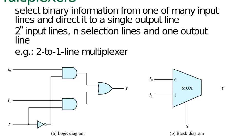
Multiplexers
select binary information from one of many input lines and direct it to a single output line
2n input lines, n selection lines and one output line
e.g.: 2-to-1-line multiplexer
Fig. 4.24: Two-to-one-line multiplexer
4-to-1-line multiplexer
Fig. 4.25
Four-to-one-line multiplexer
Sequential Circuit
D Latch
One way to eliminate the undesirable condition of the
indeterminate state in the SR latch is to ensure that inputs S and R are never equal to 1 at the same time.
Transparency latch
Race
D Q clk
X Y
Edge-Triggered D Flip-Flop
Transparency latch,
level triggered Transparency latch
JK Flip-Flop
The J input sets the flip-flop to 1, the K input reset it to 0, and when both inputs are enabled, the output is complemented. D = JQ’ + K’Q
T Flip-Flop
D = T ⊕ Q = TQ’ + T’Q
Characteristic Tables and Equations
Design Procedure
the word description of the circuit behavior (a state diagram)
state reduction if necessary
assign binary values to the states
obtain the binary-coded state table
choose the type of flip-flops
derive the simplified flip-flop input equations and output equations
draw the logic diagram
Synthesis using D flip-flops
An example state diagram and state table
The flip-flop input equations
A(t+1) = DA(A,B,x) = Σ(3,5,7)
B(t+1) = DB(A,B,x) = Σ(1,5,7)
The output equation
y(A,B,x) = Σ(6,7)
Logic minimization using the K map
DA= Ax + Bx
DB= Ax + B'x
y = AB
Fig. 5.28
Sequence detector
The logic diagram
Fig. 5.29
Logic diagram of
Excitation tables
A state diagram ⇒ flip-flop input functions
straightforward for D flip-flops
we need excitation tables for JK and T flip-flops
Synthesis using JK flip-flops
The same example
The state table and JK flip-flop inputs
JA = Bx'; KA = Bx
JB = x; KB = (A♁x)‘
y = ?
Fig. 5.31
Sequential Circuit Module
Waveform of 4-Bit Synchronous Counter
Clock
A0 A1 A2
Up-Down Counter
Up:
0000=>0001=>0010….=>1111=>0000
Down:
1111=>1110=>1101=>….=>0000=>1111
1 0
0
0 0 0
0 0 1
1
Ring Counter