Chapter 3
Improvement the Structure of Homemade Compensator and Analysis of the
Response Time
In order to compensate the polarization mode dispersion (PMD) in our polarization shift keying (PolSK) modulation system, we design a compensation compensator. The structure contains feedback circuit and control circuit. In chapter3, we analyzed and compared the polarization state with/without our homemade compensator results. However, in chapter4 we will discuss that the main factors cause our homemade compensator not perfect compensate in our WDM/PolSK system.
In this chapter, we describe the structure of homemade compensator and basic characteristics of internal circuits. The internal component contains an amplifier, a rectifier, an analogy-digital converter (A/D converter), a 8051 program and a digital-analog converter (D/A converter). They play different roles in our compensator circuit, respectively. However, this polarization compensator needs high power voltage to drive. Therefore, we design a 160V low ripple power voltage and we utilize four-channel displays to monitor the compensation result.
However, we know the circuit transmission electric message will cause
the phenomenon of transmission delay. Therefore, we will analyze the
influence of time delay on the polarization compensator system in section4-3. Because the compensation range is proportion to feedback signal, so the delay time relate to feedback. Therefore, we discuss the delay time of different compensation range and analyze the relationship between feedback signal and delay time. Finally, we analyze the total delay time effect to our compensation system and compare the compensation result with the first generation (Ⅰ) and second generation (Ⅱ). We improve the compensation delay of first generation and reduce the size of compensator. Therefore, the compensator of the second generation becomes more convenient and is applied more than the first generation.
3-1 The Structure of Our polarization Compensato r
In the compensation system, we use the feedback signal to
accomplish the close loop control feedback with polarimeter PA430. This
polarimeter analyzer can display the ellipticity and the four Stoke
parameters (S
0, S
1, S
2and S
3) in the measurement system. The
polarimeter also provides a variation voltage of feedback signal for
tracing polarization states quickly. However, in order to obtain the correct
control voltage and the feedback signal. It is very important to make the
monitoring circuits for four channels control voltage from X
1to X
4.
However, in order to observing the variation of the control signal on the
controller. We use the polarimeter (PA430) to measure the polarization states at the terminal. There is a feedback signal which can be used in the feedback control circuits of the output port with the polarimeter. The amplitude of the feedback signal will be magnified with an operational amplifier. The control chip will determine the control signals following the amplitude of the feedback signal in the polarization controller.
However, how to choose the control structure is very important which influence the result of the speed control, measure accurate and the stability. We use the single chip (AT89C51) to provide the total control signals for the polarization control device. However, the interface of signal chip and monitor circuit we use the A/D and D/A converter to connect, the black diagram is shown in Fig.3-1. The diagram of feedback is shown in Fig.3-2. The diagram of this feedback contains amplifier, rectifier and A/D converter circuits. In the next section, we will describe those circuits respectively.
3-2 Describe the Transform of Signal in the Feedback Circuit
Our compensator contains many functions of internal circuits.
Therefore, we will itemize each characteristic and analyze the
relationship between each circuit. However, in this section we not
consider the delay phenomenon of electric transmission just discuss the
characteristic of each circuit in our compensator system.
3-2-1 The Basic Characteristic of the Feedback Circuit
We know that the polarimeter provides a variation voltage of feedback signal for tracing polarization states quickly. Therefore, in the compensator system, we must to proofread the feedback signal, continuously. But, the feedback signal from monitor is very small.
Therefore, we have to amplifier it first. The circuit structure diagram is shown in Fig.3-3. From this diagram, we find the input signal is from noninverting input terminal (node1) into transmission amplifier (LF356), so we can get forward amplifier from output terminal (node2)
The feedback circuit contains a amplifier circuit, a rectifier circuit and a A/D converter. Therefore, after describing the amplifier circuit, we will continue to describe the rectifier circuit and A/D converter. After amplifing the feedback signal, we design the two half-wave rectifiers and first-order filter to rectify the AC signal. The half-wave rectifiers-formed by op amp A
1, diodes D
1and D
2and resistors R
1and R
2and the first-order filter-formed by op amp A
2,resistors R
3and R
4and capacitor C, the structure diagram is shown in Fig.3-4. Node 3 is an input signal and we can get a cut-off positive/negative half cycle at node c, node d. Finally, we can get a DC signal at node e. The measure result is shown in Fig. 3-5.
Channel is input signal “a” (node1), it is a sine-wave signal of 0.2V
peak-to-peak and frequency is 1KHz. However, channel2 is the output signal “b” (node2) of passing through transmission amplifier (LF356).
Therefore, the output will be a sine wave of 2V peak-to-peak and phase-shift 0° with respect to the input sine wave. Channel3 is the rectified signal (node c), it is the cut-off negative half cycle. By Passing through the full-wave rectifier, we can get the DC signal at node e.
Therefore, channel4 is the DC signal.
We design this structure of feedback circuit in our compensator, the main function of this circuit is to control the polarization state in the feedback control system, continuously. The picture of this feedback circuit is shown in Fig.3-6
3-2-2 The Basic Characteristic of the Control Circuit
In the control circuit, we use a pair of MSC-51 to control the
polarization state. The output ports of MSC-51 are P
0, P
1, P
2and P
3, they
control the feedback signal and connected to the input port of the set
voltage. The model number of the polarization controller is PCS-4Y,
which has 4 squeezers (Y
1, Y
2, Y
3, Y
4). It can generate control signal
from the MSC-51 micro-controller to change the voltage and control the
polarization state. The transmission rate of the D/A converter has the
most significant bit (MSB) and least significant bit (LSB). The MSB
mean that the ports of MSC-51 are P
0=P
1=FFH and the LSB mean the
ports are P
0=P
1=00H. Then, in the control board we use tunable resistance to control the DC voltage. However, four tunable resistances control the voltage of Y
1, Y
2, Y
3and Y
4of the polarization controller (PolaRiteII), respectively. The variation of input signal is proportional to the state of polarization (SOP) by increasing or decreasing the output voltage from Y
1to Y
4. The control ranges of the four axis on the poincaré sphere can be observed. The Y
1to Y
4all has it’s corresponding polarization trajectory of control range [ref]. In our control circuit, it contains Dual AT89C51 (MSC-51(1) and MSC-51(2)). The MSC-51(1) control the polarization state of change the voltage Y1 and Y2, and MSC-51(2) control the polarization state of change the voltage Y3 and Y4. From the above narrate, we can use the single chip and four channel squeezers to compensate the polarization state from arbitrary input polarization state.
The picture of the signal ship and D/A converter circuit is shown in Fig.3-7.
However, in order to obtain the correct control voltage and the
feedback signal. Therefore, after feedback and control circuit, the control
signal should be monitored by using the monitor command. We use four
channels of the potentiometer with 3-1/2 digital direct display for monitor
the feedback and control signals in the polarization control, The picture of
monitor display circuit is shown in Fig.3-8. However, the four channels
monitor display the ultimate voltage (V
1, V
2, V
3, V
4,) to control the
polarization state. The black diagram of compensation circuit is shown in
Fig.3-9.
3-3 Analysis of the Delay Time of Our Compensator System
The influence of delay phenomenon on the compensate ratio in the compensation system is very important. Therefore, we must analyze the circuit character and delay character. In this section, we will measure the each circuit about delay time and response time. However, in our measure system contain dynamic and static measure. Then, from our measure result we can find the main delay phenomenon occurred position. Finally, we will analyze and improve this factor and do my best to decrease the phenomenon of transmission delay.
3-3-1 The Static Measuring about Delay Phenomenon of Polarization Compensation
We measure the delay of each circuit and think up a method to improve our homemade polarization compensator. In this section, we measure the circuit to find the place can be improved.
3-3-1-1 The Transmission Delay in the Feedback Circuit
In this section, we will discuss the phenomenon about time delay on
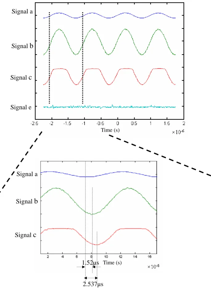
our compensate system. First, we measure the characteristic of feedback circuit and control circuit by oscilloscope (Agilent 54810A), respectively. From Fig.3-10, we will define the delay of each other.
Compare Channel2 and Channel3 signal with Channel1 signal, we find the delay are 1.52μs and 1.017μs, respectively. However, we know that channel1 is input signal ‘a’, channel2 is amplified signal ‘b’, channe3 is halt-wave rectified signal ‘c’ and channel4 is the DC signal
‘e’ of through full-wave rectifier.
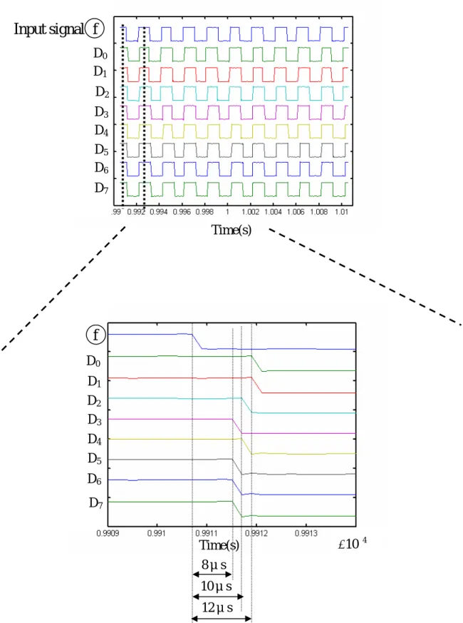
However, the DC signal injected into the A/D converter, then we will get digital signal from output 8-bit (D
0~D
7). Because the digital signal is only high or low signal, so we can not measure the delay time of it, obviously. Therefore, we analyze the reaction to injecting the square-wave ‘f’ form node7 into the A/D converter. The diagram is shown in Fig.3-11. From this figure, we can observe the output signal D
0~D
7of the A/D converter. However, the delay of signal pass through the A/D converter is shown in Fig.3-12. The D
0and D
1signals are delayed about 0.12ns, and the D
2and D
4signals are delay about 0.1ns in comparison with input signal ‘f’. However, the D
3, D
5, D
6and D
7signals are delay less time about 0.08ns in comparison with input
signal ‘f’. From Fig.4-11, we know that when the input signal pass
through the A/D converter, the maximum of delay time is 12μs.
3-3-1-2 The Transmission Delay in the Control Circuit
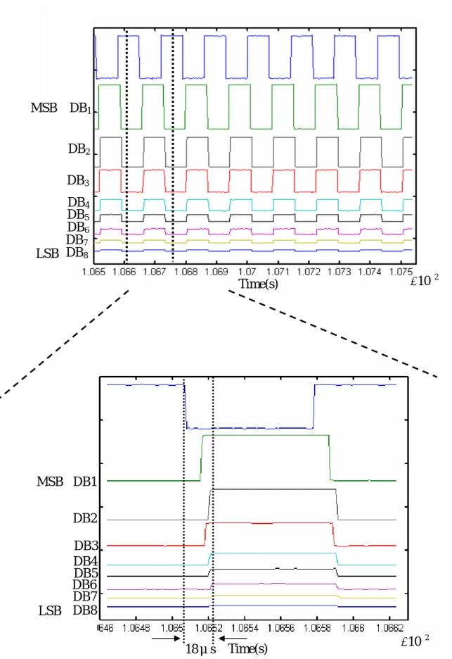
In the control circuit, we will analyze the reaction to injecting the square-wave form MSC-51 8 input ports P
30~ P
37into the D/A converter, respectively. However, in this section the emphasis exists also on the delay effect. The experimental structure is shown in Fig.3-13, the input signal is square-wave inject into D/A converter and we will measure the output signal DB
1~DB
8of B
1~B
8. However, the measure result is shown in Fig.3-14. The output signal B
1~ B
8are delayed 0s in comparison with the input signal. From this result we know that the delay phenomenon of signal pass through the D/A converter is 18μs.
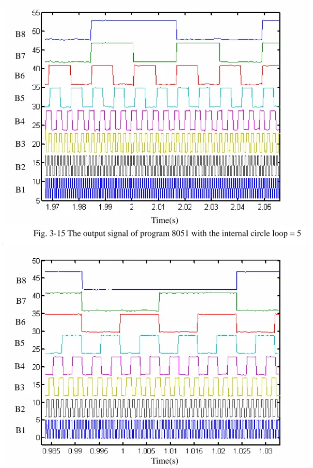
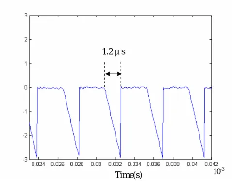
In the control circuit, we use the simple test program to test the internal circle loop of 8051 program to influence the delay on the hard-circuit. The simple programs contain loop 5 circles and 100 circles. However, we can measure the results of different circle loop, respectively. From the out ports (8 bits) of 8051 we can get the results shown in Fig.4-15 and Fig.4-16. Channel1~Channel8 (B
1~B
8) are most significant bit (MSB) and least significant bit (LSB), respectively.
However, comparing Fig.3-15 with Fig.3-16 we find that the different
circle loop do not influence the mutually delay on the output port of
8051. Therefore, we can ignore this factor will cause the phenomenon of transmission delay. However, we can form the output port of D/A converter to find the relationship of signal delay and the number of circle loop in the 8051 program. The results are shown in Fig.3-17and Fig.3-18. Form those results, we can find the circle number is a key point because the number of compensation loop will influence the compensating result and the phenomenon of transmission delay. When the circle loop =100, the compensation result will better than the circle
=10 but the delay time also larger than the circle =10. Therefore, we will find the optimum condition between the compensation result and
delay time. In our 8051 program the maximum delay is about 64μs.
However, the output signal of D/A convert transmitted to the amplifier (LF353). Then we will compare the converted result with this result of going through the amplifier in Fig.3-19. From this result we can find the there is no delay phenomenon when the signal pass through the OP amp.
From above measure results, we will emphasis on researching
feedback circuit because it is the main reason cause delay phenomenon
on our compensate system. The delay of 8051 programs is fixed when
the program is accomplished. Moreover we have found the optimum
condition of internal program. Therefore, how to reduce the delay of
feedback circuit is become a most important topic. Besides, the length
of the data bus is also a key point about transmission delay. But the
delay tine of A/D converter and D/A converter can be neglected, because the delay time of they are smaller than the delay time of amplifier and rectifier. Therefore, in the next section we only discussion the relationship between the delay and the each component in the feedback circuit.
3-3-2 Analyzing the Delay Time of Each Component in the Feedback Circuit
From measuring result, we know that the feedback circuit caused the delay is much serious than the control. Therefore, we will analyze the components contain capacitance and amplifiers (LF356N and TL082) in the feedback.
We know the total delays contain capacitance charge /discharge, wiring route of circuit, heat effects and limited by each component.
Therefore, we will eliminate the not important reason and find the main factor occurs the phenomenon of transmission delay. In our measure result we can in detail analyze about delay of each component. The capacitance will cause delay in the process of change and discharge.
However, the material and the value of capacitance will influence on the
delay time. We can compare the delay results with different value, the
result shown in Fig.3-20. From this result we get an important
information, we can select the best value of capacitance and utilize the
better material to reduce the delay time. However, in order to getting the
good effects of amplifier and rectifier circuits the values of capacitances are 10μF so the total delay caused by the capacitance is about 0.15μs in the feedback circuit.
In the feedback circuit, we also measure the delay time of OP (LF356N) and OP (TL082), the results are shown in Fig.3-21 and Fig.3-22. The total delay in the feedback is 2.537μs, deduct the delay of capacitance and OP. Then, the remain delay is caused by the wiring route. Therefore, the result of wiring route also an important factor of the delay time. Besides, the length of data bus also a serious factor. We know when the output signal of the feedback circuit was connected to the control circuit also has the delay phenomenon. From the basic theory of the physics, we know the velocity of electric is about 5.9×
10
5m/s. In our system, the length of the data bus connected to feedback circuit and control circuit is about 3cm. Therefore, the delay time can be calculated utilizing equation (4.5)
v s
T L 0 . 5 10 0 . 05 µ
10 9 . 5
10
3
75
2
= × ≅
×
= ×
=
− −(4.5)
where L is the transmission distance, v is the transmission velocity and T is the necessity of transmission time. However, the relationship between the delay time and the length of data bus is shown in Fig.3-23.
Form theoretical result and formula we know that the length of data bus
causes transmission delay seriously and from experimental result we also
verify this contention. The size of circuit board is an important factor of
our discussion, because it influence on delay and response time of our compensator.
Therefore from above describe, we can calculate the total delay of our polarization compensator (second generation) and compare the total delay with the first generation under the compensation condition. The block diagram is shown in Fig.3-24 and Fig.3-25. Fig. 3-24 is about total response time of first generation and Fig. 3-25 is about total response time of second generation. From Fig.3-25 we know the response time of the polarization compensator (second generation Ⅱ ) is 96.9 μ s.
Compare Fig.3-24 and Fig.3-25, we have improve the serious delay in the second generation of our polarization compensator. The delay time can be reduced from 149.88 μ s to 96.9 μ s, and the variation range of polarization state also be restrained, the variation can be reduce from 24°
to 15°. The results are shown in Fig. 3-26 (a) to (c). Fig. 3-26(a) is the polarization state without turn on our compensator, the variation of polarization state is very large is about 32°. Fig. 3-26(b) is the result of turn on the compensator (first generation Ⅰ ) and the variation of polarization state is reduced to 24°. Fig. 3-26 (c) is the compensation result of compensator (second generation Ⅱ) the polarization state can be effective stable. The variation of polarization can be reduced from 32°
to 15°. Comparing with compensation result, the compensator Ⅱ is
better than compensator Ⅰ. Because compensator Ⅱ more effective to reduce the variation of polarization state than compensator Ⅰ.
3-4 The Dynamic Measuring about Delay Phenomenon of Our Compensation System
After static measure, we can measure the actual delay in the compensation system. In our compensation system, we use the feedback signal with the polarimeter PA430 to accomplish the close loop control.
The polarimeter will provide a variation voltage of feedback signal for tracing polarization states quickly. Therefore, we will analyze the response of our polarization compensator. However, from section 4-3 describe we know that the main delay phenomenon is occurred in the amplifier circuit, rectifier circuit, 8051 program and data bus. Therefore, we only analyze and measure the delay of feedback circuit in the compensation system.
The feedback signal of feedback circuit is the message of variation
in the polarization state, and it wait to be amended and controlled. If we
use our polarization compensator to compensate the polarization state, the
compensation range is shown in Fig.3-27. We know that in the
compensating process will cause the transmission delay. However, the
delay phenomenon will limit the compensate result. The delay time of
feedback signal passing through the homemade compensate circuits is
equivalent to the response time of our polarization compensate system.
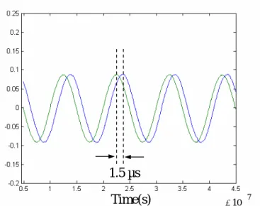
The delay of polarization compensate system in the tiny variation of polarization state (A-A’) is shown in Fig.3-27. Its variation of orientation is about 10°. From this result Fig.3-28 (a) (b), we know the delay time of amplifier circuit and rectifier circuit is about 1.49μs in the generationⅡ compensator and the delay in the feedback circuit of generation Ⅰ compensator is 24.17μs .
However, compensating the range of polarization state trajectory on the poincare sphere from B to B’, the delay phenomenon also be occurred.
The variation of orientation from B to B’ is about 30°. However, if we will compensate the polarization state on this range the delay time is shown in Fig.3-29 (a), (b) From this result, we find the delay time of amplifier circuit and rectifier circuit is about 15.27μs and 40.3μs in generationⅡ and compensatorⅠcompensator, respectively.
After analyzing the delay phenomenon of compensation compensate system in the tiny variation of polarization state. We will analyze the delay phenomenon of polarization compensation system in the large variation of polarization state (C-C’). The compensation range is as 50°
shown in Fig.3-27. However, the delay time of compensating process is
shown in Fig.3-30. From this result, we find the delay time of amplifier
circuit and rectifier circuit is about 22.42μs and 58.7μs in generationⅡ
and generationⅠcompensator, respectively.
From those results, we find we can reduce the delay phenomenon, substantially. Besides, we raise the value of DOP and reduce the variation of ellipticity, the result is shown in Fig.3-31. From this result, we find the compensation result of generationⅡ is better than generationⅠ. And the performance of polarization compensation is inverse proportion to the compensation range.
This result shows the relationship with compensation range of feedback signal and the transmission delay. From the practical measure results, we find the relationship with feedback signal from monitor computer and the delay time. However, the curve line is shown in Fig.3-32. In our polarization compensation system, the feedback signal is the inaccuracy signal, it is need to be corrected. Therefore, if we want to change the polarization state, the feedback signal will has variation by a street. The value of feedback signal is varied with the polarization state.
From Fig.3-32, we can find the transmission delay has been restrained, and the compensation range also be raised.
3-5 Summary
In this chapter, we measure the characteristic of individual circuit
and analysis the time delay phenomenon. In our polarization
compensation system, the value of feedback signal will be influenced by
the delay phenomenon. However, the total delay time contains the delay of amplifier circuit, rectifier circuit, A/D converter, 8051 program and data bus. We compare the response time of dynamic results with first generation and second generation, roughly. From this result, we find that the delay time is increased with the voltage of feedback signal. However, the feedback signal was proportional to the compensation range of polarization compensator. Therefore, the delay phenomenon is more evident when the range of compensate is larger. Finally, comparing second generation with first generation compensator we can raise the compensation result.
Under the same compensation range, the second generation compensator reduce the total response time from 149.88μs to 96.9μs and reduce the variation of compensation rang from 24° to 15°. Besides, the performance of compensation result in generationⅡ is better than generationⅠ.
Comparing with the first generation of polarization compensator, we
curtail the circuit board and decrease the delay time of compensation
system. Therefore, we can more effective compensate the transmission
system and improve the transmission quality.
160V low ripple power
Four section fiber squeezed automatic polarization
controller
Polarization SOP analyzer
Feedback circuit AT89C51
microcontroller CW Laser
Fig.3-1 The block diagram of our designed polarization controller Compensator
A area
Amplifier circuit
B area
Rectifier circuit
C area
ADC0804 Vcc CLK R
DB0
DB7 +5
A/D converter circuit
90K
10K
+15
-15 3.3K
OP
LF 356N
Fig.3-2 The diagram of the feedback circuit +15
-15 OP
OP
Fig.3-3 The design structure of the amplifier circuit
B areas
90K
10K
A areas
signal
Input signal a
Output signal b LF 356N
OP
10μF 10μF
3.3K
+ Node1
Node2 R
1R
210μF 10μF
3.3K
B area
+15 -15
A area
Input signal b AC
c d
e
A
1A
2D
1D
2R
1R
2R
3R
4C
+
+ Node3
Node4 V
1
Nodet5
Node6
V
2Fig.3-4The design structure of the rectifier circuit
Fig.3-6 The picture of feedback circuit contain A/D converter and feedback display
Fig3-5 The transform result in the feedback circuit Signal a
Signal b
Signal e
Signal c
Fig.3-7 The control circuit of pair 8051 and D/A converter
Fig.3-8 The picture of the four channels display monitor circuit
Fig.3-9 The diagram of control the feedback signal and display the Controlled voltage
Polarimeter
D/A converter D/A converter
8051 Program 8051 Program A/D converter
PolaRite Ⅱ
Laser source
Feedback circuit
Signal a
Signal b
Signal e
1.52µs
2.537µs
Fig. 3-10 The measured result of the transmission delay occurred in the feedback circuit
Signal c
Signal a
Signal b
Signal c
Time (s)
Time (s)
C area
ADC0804 Vcc CLK R +5
B area
A area Input signal f Node7
D0
D7
Output signal D
0~D
7Fig.3-11 The structure of the A/D converter circuit
12μs
Fig. 3-12 The measured result of the transmission delay occurred in the signal pass through the A/D converter
D
0D
1D
2D
3D
4D
5D
6D
7Input signal f
Time(s)
D
0D
1D
2D
3D
4D
5D
6D
7f
10μs 8μs
Time(s) × 10
−4Fig.3-13 The structure of the MSC-51 and D/A converter circuit +5V
DAC0800 V
02K 2K
-5V
8051 P30 P31 P32 P34 P33 P35 P36 P37
X1 X2
P00 P02 P03 P05 P06 P07 P04 P01
P20 P22
P26 P24 P21 P23 P25 P27 B1
B3 B4 B6 B8 B2
B5 B7 MSB
LSB +
_
I
outOutput signal
DB8 DB4 DB3 DB2
DB6 DB5 DB7 MSB DB1
LSB
Fig. 3-14 The transmission delay occurred in the signal pass through the D/A converter
MSB DB
1DB
8DB
7DB
6DB
5DB
4DB
3DB
2LSB
Time(s)
Time(s)
10
−2×
10
−218μs ×
Fig. 3-15 The output signal of program 8051 with the internal circle loop = 5 Time(s)
B8 B7 B6 B5 B4 B3 B2 B1
Fig. 3-16 The output signal of program 8051 with the internal circle loop = 100 Time(s)
B8
B7
B6
B5
B4
B3
B2
B1
Fig. 3-17 The response time with circle loop =10 of 8051 programs
Fig. 3-18 The response time with circle loop =100 of 8051 programs
10-3
1.2μs
10-3
12μs Time(s)
Time(s)
Fig.3-19 The delay time of signal from D/A converter pass through the amplifier LF353
Time(s)
Time(s)
Fig. 3-20 The delay time of capacitance with different capacitance value (a) The capacitance value is 100μF
0.8 µs 1 µs
10−7
×
(b) The capacitance value is 271μF
0.15µs
10−7
×
(c) The capacitance value is10μF (d) The capacitance value is 47μF
10−7
×
10−7
×
1.5 µs
Time(s) Time(s)
Time(s)
Time(s)
10−6
0.15µs
×0.23µ s
10−6
×
Fig.3-21 The response time of amplifier TL082
Fig.3-22 The response time of amplifier LF356N Time(s)
Time(s)
Theory result Experimental result
Fig.3-23 The relationship between the delay time and the length of data bus
26μs D/A converter 8051
Program A/D
converter Rectifier
circuit Amplifier
circuit
Feedback circuit Control circuit
Data bus
4.67 μs 6.54μs 24μs 1.67μs 87 μs
149.88μs
Fig.3-24The compensation response of PMD compensator (First GenerationⅠ)
Fig.3-26 (a) The polarization state without compensated with our PMD compensator
32°
Fig.3-26 (b) The compensation result with PMD compensator (Ⅰ)
24°
D/A converter 8051
Program A/D
converter Rectifier
circuit Amplifier
circuit
Feedback circuit
Control circuit
Data bus
1.524 μs 1.017μs 12μs 0.36μs 64 μs 18μs
96.9 μs
Fig.3-25 The compensation response of PMD compensator (Second GenerationⅡ)
Fig.3-27 The diagram of different compensation range with our PMD compensator
A′
C′
C B
B ′ A
Fig.3-26 (c) The compensation result with PMD compensator (Ⅱ)
15°
Fig.3-28 The delay time of compensating the variation range of orientation about 10° with our PMD compensator
10
−80.85μs ×
1.49μs Time (s)
24.17μs
(b) GenerationⅠ Compensator
(a) GenerationⅡ Compensator
15.27 μs Time(s)
Fig.3-29 The delay time of compensating the variation range of orientation about 30° with our PMD compensator
Time (s)
40.3μs
10−3