Formation and characteristics of silicon nanocrystals in plasma-enhanced
chemical-vapor-deposited silicon-rich oxide
Chi-Fa Lin
Advanced Process Development Division, Winbond Electronics Corp., Hsinchu 300, Taiwan
Wei-Tsu Tsenga)
Department of Materials Science and Engineering, National Cheng-Kung University, Tainan 701, Taiwan
Ming Shiann Feng
Department of Materials Science and Engineering, National Chiao-Tung University, Hsinchu 300, Taiwan
共Received 7 May 1999; accepted for publication 1 December 1999兲
The formation of nanosized Si crystals in dual-frequency plasma-enhanced chem-ical-vapor-deposited silicon oxides is identified in this study. As a higher SiH4N2O gas flow rate
ratio is employed during the deposition process, the silicon-to-oxygen atomic ratio and the dangling bond density both increase. The resulting oxide films contain more Si–H bonds and less Si–O and Si–O–H bonds, as determined from the Fourier-transform infrared spectra. The main type of charge defects in these oxides change from"SiwO3bonds (E
⬘
centers兲 to "SiwSi3bonds, which eventuallycluster together and precipitate out from the oxide network to form the Si nanocrystals. The size of these Si nanocrystals falls within the range of 30–50 nm, as observed by high-resolution transmission electron microscopy. The formation of these nanocrystals inside the silicon-rich oxides results in a lower film density, a tensile stress component, and a higher wet etching rate, even under the ion bombardment provided by the rf bias power during deposition. The underlying mechanisms for the formation of these Si nanocrystals from the silicon oxide will be proposed. © 2000 American Institute of Physics. 关S0021-8979共00兲08905-2兴
I. INTRODUCTION
Silicon oxide has been utilized as the standard material for electrical isolation in microelectronics. The characteris-tics of this material have been demonstrated to depend strongly on the deposition methods. Among the various pro-cessing methods for silicon oxide, plasma-enhanced chemi-cal vapor deposition 共PECVD兲 and its other versions have been utilized most extensively to deposit silicon oxide for use in intermetal dielectric. The characteristics of the depos-ited oxide can be fine tuned to meet the specific requirements for device performance improvement. For example, the in-troduction of a higher dangling bond density to the interlayer dielectric 共ILD兲 oxide by incorporating more Si–H bonds into the structure has been an effective way to enhance hot carrier lifetime for memory devices.1–3 The extra dangling bonds may act as trap centers for hydrogen and moisture released from neighboring nitride or oxide layers, protecting the active device underneath. Results of previous studies in-dicate that these extra Si–H bonds may exist in different bonding configuration within the oxide network, depending on the amount of Si–H bonds incorporated. As Si–H bonds are being introduced to the oxide, the Si atoms may first attached to the oxygen to form"SiwO3 bonds (E
⬘
centers兲,which are converted to"SiwSi3bonds later as even more Si
atoms are present.4 The latter may exist in form of Si microcrystals,5 although this has not been verified experi-mentally.
In this study, we analyze the chemical characteristics and bonding configurations of PECVD silicon-rich oxides. The existence of nanosized Si crystals in these oxides will be identified and the mechanisms leading to the formation of these Si nanocrystals from their parental oxide network will be proposed.
II. EXPERIMENT
The oxide thin films were deposited on 150 mm共100兲 Si wafers in a dual-frequency PECVD reactor at 400 °C with a pressure of 2.2 Torr, employing SiH4⫹N2O gas chemistry. A
low-frequency共375 kHz兲 rf power was applied onto the wa-fer surface to enhance ion bombardment on the as-deposited films so as to improve the film quality, whereas a high-frequency 共13.56 MHz兲 rf power was applied onto the gas inlet to decompose the SiH4⫹N2O gas mixtures. The
SiH4:N2O flow rate ratio was varied in order to introduce
different Si content into the oxide deposited.
The chemical wet etch rate of oxides was tested using 10:1 NH4F buffered HF oxide etcher 共10:1 BOE兲 solution. To monitor the wet etch rate, film thickness was measured before immersing the samples into the 10:1 BOE chemical solution for 2 min. After the immersion, the samples under-went standard cleaning process of rinse, drying, and then post-etch thickness measurements.
Standard wafer curvature measurement technique was used to determine the stress,, based on Stoney’s equation for a film of thickness tf:
a兲Electronic mail: [email protected]
2808
⫽共1⫺E兲 ts
2
6Rtf
, 共1兲
where E, , R, and ts are, respectively, Young’s modulus, Poisson’s ratio, radius of curvature, and thickness of sub-strate. The thin film stress is calculated by subtracting the original radius of curvature of the wafer to obtain the net radius of curvature change due to the thin film process, given known Si Young’s modulus and thickness. In this study, tf is maintained at 500 nm for stress measurements.
The film density is determined by microbalance, where the weight of samples was measured at preprocess and post-process steps. Once the thin film thickness was measured by interferometer and the weight difference between pre/post process was known, the film density can be calculated given the constant wafer surface area.
The hydrogen concentration in PECVD oxides was char-acterized by room temperature infrared 共IR兲 absorbance method within the wave number range from 4000 to 400 cm⫺1, using a Biorad QS 300 Fourier-transformation IR 共FTIR兲 spectrometer with a CsI beam splitter. Bond densities are calculated from FTIR peak areas of the respective bond signals and chemical bond configuration is investigated from FTIR absorption peak positions. Every unprocessed virgin wafer was prescanned before deposition as the background to ensure that the post-deposition scanning results were merely due to the spectral difference between the dielectric films. Each sample was scanned 64 times and the resulting spectra were averaged for accuracy concern. The film thickness for FTIR analysis is 500 nm and the resolution of IR spectrum was about 4 cm⫺1.
The Si:O atomic ratio was determined by electron probe x-ray microanalyzer 共EPMA兲 with the model JEOL JXA-8800M analyzer. The electron beam accelerating voltage was maintained at 15 keV with a 2.8⫻10⫺8amp current. This
corresponds to a maximum depth of approximately 1500 nm. The Si dangling bond ("SiwSi3) density was measured by electron paramagnetic resonance spectrometer 共EPR兲 con-ducted with a Bruker EMX-10 spectrometer under a center field of 3489.9 G with width of 50 G. The microwave fre-quency was set at 9.779 GHz with a power of 19.971 mW. The receiver modulation frequency and its amplitude were 100 kHz and 1.6 G, respectively. The sample thickness for EPMA and EPR analyses are 2000 nm with less than 2% variation. For EPR analysis, the influence of Si substrate and sample edge was included. However, precise control over the sample size共less than 1000 nm linear variation兲 ensures the relative peak difference between SRO and Si substrate. Fi-nally, both high-resolution transmission electron microscope 共HRTEM兲 and atomic force microscope 共AFM兲 were em-ployed to observe the microstructure and surface topography of the silicon-rich oxides.
III. RESULTS AND DISCUSSION
A. Characteristics of silicon-rich oxides
Results of material characterization for the PECVD ox-ides used in this study are listed in Table I. The SiH4:N2O gas flow ratio increases from samples SRO1 to SRO5 and the Si–H peak height 共from FTIR spectra兲 also increases correspondingly. Meanwhile, the O:Si atomic ratio as deter-mined from the decreases of EPMA suggesting that the ox-ides are becoming more Si rich. The low/high radio fre-quency power ratio is also shown in Table I. From the density data shown, it is observed that the application of a low-frequency bias power on the substrate electrode tends to density the oxide films at first 共SRO2 and SRO3兲, but the effect is overwhelmed later by other operating mechanisms which cause the reduction in density again 共SRO4 and
TABLE I.共a兲 Deposition conditions of dual-frequency PECVD oxide films and 共b兲 materials characteristics of dual-frequency PECVD oxide films used in this study.
Item Unit SRO1 SRO2 SRO3 SRO4 SRO5
a
Conditions SiH4:N2O ratio 0.05 0.06 0.08 0.1 0.13
RF power ratio LF/HF 0 0.67 0.82 1 1.22
b
RI 1.46 1.51 1.54 1.56 1.67
EPMA atomic ratio 共O/Si兲 2 1.46 1.46 1.43 1.28 Dangling bond ratio Normalized w.r.t.
SRO1
1 1.1 1.4 3.4 4.3
AFM roughness nm 2.94 3.32 3.99 4.02 4.15
Post etch roughness nm 2.71 NA 4.49 NA 6.52
BOE E/R nm/min 223 120.7 156.5 179.8 186.6
Stress MPa 530 ⫺680 ⫺44 62 137
Density g/cm3 2.17 2.18 2.26 2.17 2.10
H2O release wt % 1.58 0.87 0.75 0.63 0.51
Si–O stretch cm⫺1 1065 1049 1041 1035 1032
Si–O peak height NA 0.811 0.693 0.644 0.609
Si–H cm⫺1 NA 2272 2252 2245 2241
Si–H peak height NA 0.029 0.042 0.073 0.09
Si–O–H cm⫺1 NA 3385 3383 3377 3372
Si–O–H peak height NA 0.014 0.013 0.013 0.001 LF⫽low frequency; HF⫽high frequency. NA: Not analyzed.
SRO5兲, even if a higher LH/HF power ratio, i.e., heavier ion bombardment, is employed in the latter case. This point will be elaborated later in the discussion.
As the SiH4/N2O gas ratio increases from SRO1 to
SRO5, the refractive index共RI兲 increases from 1.46 to 1.67 monotonically, regardless of the rise and fall of density as described above. The above result is similar to the previous report by Jain et al.,5although no proper account was given. According to the Lorentz–Lorenz model and the Gladstone– Dale model, there is a linear relationship between the RI and film density.6 Therefore, the increase in RI from SRO1 to SRO5 in the present study should result from other factors that overshadow the density effect.
Regarding the chemical characteristics of oxides, the in-crease in silicon content from SRO1 to SRO5 also translates to an increase in BOE wet etch rate. Such an increasing trend in wet etch rate cannot be explained by the film densification effect resulting from intensified ion bombardment, since the latter should give rise to a reverse trend,7i.e., decreasing wet etch rate from SRO2 to SRO5. It should be, instead, the consequence of the changing chemical bonding and compo-sition in the oxide films, as will be discussed later in greater details. The high etch rate of SRO1, on the other hand, seems to be a direct consequence of the lack of ion bombardment, since, in this case, no low-frequency rf power was applied onto the wafer during deposition.
The mechanical stress of SRO samples is also recorded in Table I. For silicon oxide film deposited on具100典 Si, the extrinsic stress resulting from thermal expansion mismatch is about-40 MPa for 400 °C deposition temperature. Therefore, the stresses measured in the present study should result mainly from changes in film microstructure or impurity, in other words, they are intrinsic stress. Without the rf bias power, the as-deposited SRO1 oxide attains a high tensile stress. The application of a rf power reverses the stress state to high compressive. However, the stress shifts back to the tensile direction as a greater rf power is applied. Again, the change in structure and bonding configuration may be the key to the change in mechanical stress. Also noted is that there appears no direct correlation between the trends in stress and BOE wet etch rate. In fact, the typical mechanical stress in oxides translates to an energy on the order of 10⫺5eV,8far less than the bond energy of Si–O. Therefore, the existence of mechanical stress in the oxide network would contribute directly to the weakening of Si–O bonds and hence to the chemical etching rate. One previous study reported that the relief in compressive stress would result in a corresponding increase in water diffusion rate in the glassy film and hence a higher dissolution or hydration rate 共wet etching rate兲 in the BOE solution.9This may explain, at least partially, the change in etch rate in the present case. The bond strain makes the oxide more reactive and porosity pro-vides a higher surface area for holding water molecules and easy access for it to reach the reaction sites.
B. Change in bonding configuration and the formation of Si nanocrystals
All the results above suggest that ion bombardment alone cannot account for the change in characteristics of the
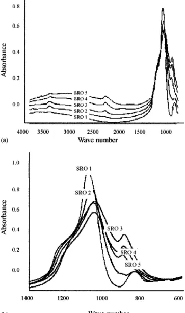
oxides. Instead, chemical effects, i.e., changes in composi-tion and bonding configuracomposi-tions seem to be the dominant factor. In light of this, material characterization work is per-formed to analyze the structure and composition of the oxide films. FTIR spectra of the as-deposited SRO films are shown in Fig. 1共a兲. The peak position of Si–O–Si bonds and its intensity are enlarged in Fig. 1共b兲. The shifts in peak position and relative peak height of the three different bonds are also summarized in Table I. As can be seen, Si–O–Si 共stretch兲, Si–H, and Si–O–H bands all move to lower wave numbers as more Si is present in the films. Note that for stoichio-metric SiO2, the Si–O–Si stretch band should be positioned
around 1067 cm⫺1, corresponding to a RI of 1.452. The lower wave numbers for Si–O–Si stretch band in the silicon-rich oxides共SRO兲 also correspond to their higher RI. Mean-while, Si–O stretching band frequency decreases to lower wave number as the film becomes more silicon rich. In terms FIG. 1. 共a兲 FTIR spectra show that the bonding density of Si–OH and Si–O–Si decreases while that of Si–H increases. The peak position shifts to lower wave numbers for Si–O–Si共stretch兲, Si–H, and Si–O–H bands, as SiH4gas flow rate increases during deposition.共b兲 Enlarged FTIR spectra
show the peak position of Si–O–Si共stretch兲 shifts to lower wave numbers with a decrease in intensity.
of peak intensity, both Si–O–Si and Si–O–H bond densities decrease while Si–H bond concentration increases slightly. This suggests that the additional Si atoms are incorporated in form of Si–H bonds into the oxide network. The peak posi-tion also shifts due to this change in chemical composiposi-tion. In addition, the reduction in the density of Si–O–H bonds and hence the hydroxyl groups leads to the decrease in mois-ture content of the film, as evidenced from the decrease in % H2O release listed in Table I.
The EPR spectra of the SRO films are exhibited in Fig. 2. As the silicon content increases from SRO1 to SRO5, the type of dominant defect species present in the oxides also changes. For SRO1, SRO2, and SRO3, a peak with a G value equal to 3489 can be clearly observed, although its intensity follows a declining trend. This corresponds to the character-istic spin of E
⬘
centers ("SiwO3), which are the dominantdefect species in these oxides. For SRO4 and SRO5, how-ever, the E
⬘
centers disappear and a new peak with a G value of 3482.5 emerges. This coincides with the peak of Si spin centers ("SiwSi3).4
Overall, as the Si to O atomic ratio in-crease from the stoichiometric value of 0.5 to 0.73 for SRO5, the dominant defect spin centers shift from the E
⬘
centers to Si spin centers, as extra silicon atoms are incorporated into the oxide. The increase in the number of nonbonded Si atoms would introduce a higher Si dangling bond ("SiwSi3)den-sity in the oxide.
This shift in the dominant defect species from E
⬘
centers ("SiwO3) to Si dangling bonds ("SiwSi3) with increasing Si content in the oxide films suggests that there is a major change in the oxide structure from SRO1 to SRO5. The re-placement of Si–O–H and Si–O bonds with Si–H bonds results in the reduction of the number of E⬘
centers in the oxide. Meanwhile, the existence of more and more"SiwSi3bonds raises the possibility of forming Si clusters in the ox-ides. The existence of such Si clusters or nanocrystals in the silicon oxide network has been discussed before,10 but has never been directly identified and characterized. In fact, most of the previous works on Si nanocrystals focused on the for-mation and photoluminescence properties of porous Si 共por-Si兲 from bulk Si wafers by anodic etching with HF.11In the present study, efforts were spent on the identification and
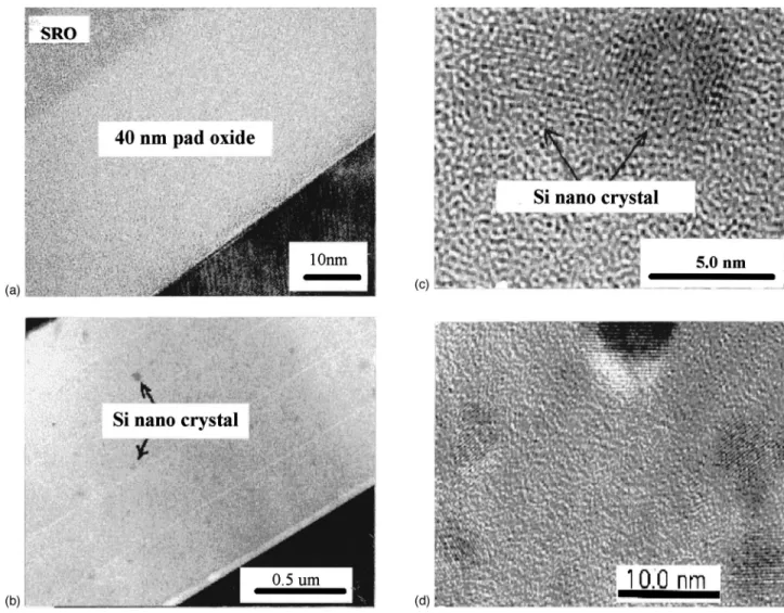
characterization of Si nanoscrystals inside the oxides. Figure 3共a兲 is the bright-field 共BF兲 HRTEM micrograph showing the interface between the thermally grown pad ox-ide and PECVD SRO3 silicon-rich oxox-ide. The sharp contrast along the interface suggests that the structures of the two oxides are quite different. Figure 3共b兲 is the BF HRTEM image of SRO3. The black dots in the oxide film are the possible sites of the Si clusters. A closer look at these black dots 关Fig. 3共c兲兴 reveals the short-range order of atomic ar-rangement in these Si clusters, implying that they are crys-talline in nature. These Si clusters or nanocrystals, about 30–50 nm in dimension, are more abundant in the silicon-richer SRO5, although their size remains virtually unchanged 关Fig. 3共d兲兴. Electron-beam microdiffraction was also per-formed at these Si nanocrystals. However, due to the small sample size, the signals are quite weak and therefore, the crystallographic planes could not be clearly indexed.
The roughness measurements using AFM provide fur-ther evidence for the existence of these Si nanocrystals. From the data in Table I, the roughness of SRO increases with the increasing Si content. This may result from the existence of the Si nanocrystals, as more of them are present in the Si-richer oxides. A typical AFM image of the SRO is depicted in Fig. 4共a兲 for SRO5. After BOE wet etching, the roughness of SRO1 共nearly stoichiometric兲 remains virtually un-changed, while that of silicon-rich oxides increase signifi-cantly, as can be observed in Fig. 4共b兲 for SRO5 after etch-ing. Since the BOE etchant has a high oxide-to-Si selectivity, it preferentially attacked the oxide in SRO5, leaving behind the Si nanocrystals on the surface and resulting in the higher roughness after etching.
C. Characteristics of Si nanocrystals inside the oxide
The existence of these Si nanocrystals alters the charac-teristics of the silicon-rich oxides significantly, as illustrated by the post-etch roughness change described above. Basi-cally, the silicon-rich oxides can be perceived as a mixture 共or alloy兲 of near-stoichiometric silicon oxide and Si nanoc-rystals so that its overall characteristics bear those of oxide and Si.
The introduction of more Si atoms to the silicon oxide network also alters the optical and dielectric characteristics as well. When an external electric field E causes a slight displacement x of an electron cloud with a charge q on an atom, the induced dipole moment m is simply qx. The elec-tronic polarizability, aecan then be expressed as
␣e⫽ qx
E . 共2兲
Assuming that electrons are elastically bound to the nucleus, the charge displacement can therefore be related to the inter-action force between electrons and the positive nucleus so that:
qE⫽kx, 共3兲
FIG. 2. EPR spectra of SRO films show the increase in electron spin density and shift in g factor with increasing Si content from SRO1 to SRO5.
where k is the force constant which represents the force per unit length needed to displace the electrons from the nucleus. Substituting Eq.共3兲 into Eq. 共2兲 yields an alternative expres-sion for electron polarizability:
␣e⫽ q2
k . 共4兲
The electronegativity of O, Si, and H is 3.6, 1.8, and 2.2, respectively. An atom with a low electronegativity 共e.g., Si兲 will also have a small force constant k, since the nucleus has weak affinity for electrons. As a consequence, as more Si is incorporated into the oxide network, the electron polarizabil-ity is enhanced according to Eq.共4兲. The electronic polariza-tion ke, and hence the refractive index increases correspond-ingly.
Based on the perspectives above, the continuous rise in RI from that near the stoichiometric oxide 共SRO1, RI⫽1.46,) to 1.67 of SRO5 should be the direct consequence of increased silicon content, instead of the densification ef-fect in the deposited oxide films. In fact, the density de-creases, not inde-creases, with increasing Si content in the ox-ide. This finding is similar to the one previous study by Jiang
et al.,1who attributed the change of RI in annealed PECVD oxides to the alteration in Si–O bond chemistry rather than densification in oxide network.
The inclusion of observed Si nanocrystals in the oxide network also causes a major change in the macroscopic stress as shown in Table I. Despite the application of rf bias that provides ion bombardment during deposition, the me-chanical stress in the silicon-rich oxide films becomes pro-gressively tensile, as more Si–H bonds are being introduced to the oxides. It should be noted that Si–H can be present in four different configurations in suboxides as H–Si–Si3⫺nOn for n⫽0 to 3.12For nearly stoichiometric but slightly silicon-rich oxide, n⫽3 is the more likely bonding configuration for which the local environment of the Si atom is almost identi-cal to that of the Si atom in stoichiometric silicon dioxide. In this case, strain in the oxide is compressive, resulting from the ion bombardment during deposition. As more Si–H bonds are being introduced to the oxide, n reduces to 2 or even 1 and the oxide assumes a more Si-rich configuration with a slightly more open structure locally, since the exis-tence of more Si–H bonds would disrupt the s p3 O–Si–O tetrahedra. Meanwhile, the oxygen atom that is consumed in
FIG. 3. 共a兲 HRTEM image showing the contrast between the thermally grown pad oxide and PECVD silicon-rich SRO3. 共b兲 HRTEM image showing the existence of Si crystals共black dots兲 inside the PECVD SRO3. 共c兲 A closer look at the Si crystals in Fig. 2共b兲. Si atoms are arranged in ordered crystalline fashion inside the Si crystals.共d兲 HRTEM image showing the Si crystals in SRO5 oxide.
the process would react with hydrogen to form hydroxyl groups, which escape from the oxide network, giving rise to the low % moisture release as detected by thermal desorption spectroscopy共TDS兲. From the FTIR spectra in Fig. 2共b兲, the observed shift in the Si–O stretching peak to lower wave number positions with a corresponding reduction in its inten-sity in the Si-richer oxides suggests that the Si–O stretching
peak is associated with strained bonds. The incorporation of additional adsorbed Si–H bonds into the film tends to inhibit perfect growth locally leading to elongated bonds and/or ex-tra silicon dangling bonds and hence a tensile stress component.13The chemical reactivity and etch rate, in turn, increase correspondingly. As a consequence, the formation of Si nanocrystals is catalyzed by the strained Si–O bonds and the resulting SRO films exhibit higher wet etching rates. As to the density change in the SRO films, the ion bom-bardment effect dominates first as Si–H bonds are being in-troduced to the oxide. This leads to an overall increase in density from SRO1 to SRO3. As enough Si–H bonds are present and Si nanocrystals are precipitating out from the oxide, the induced open structure overwhelms the ion bom-bardment effect and leads to a reduction in density in SRO4 and SRO5. The above density change also goes hand in hand with the change in dangling bond density, as shown in Table I. The high dangling bond density in SRO4 and SRO5 is associated with the "SiwSi3bonds in the nanocrystals.
The observation that the Si nanocrystals become more abundant but do not grow in size as more Si–H bonds are being introduced implies that the formation of Si nanocrys-tals is limited by the growth, instead of nucleation process. Once the nanocrystals have grown to a certain size, the sur-rounding oxide network inhibits further growth of them. More experimental work is undergoing to verify this point.
D. Comparisons between single-frequency and dual-frequency oxides
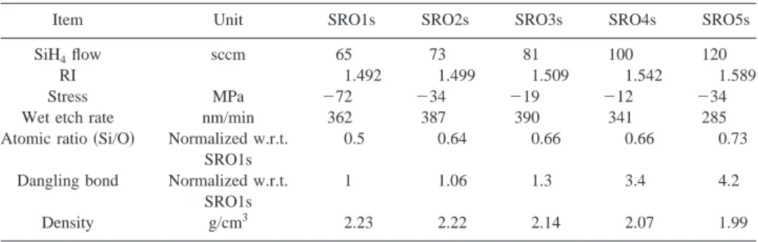
To further investigate the impacts of higher SiH4 gas
flow and bias rf power on as-deposited oxide film character-istics, single radio frequency 共13.56 MHz兲 power deposited PECVD silane oxides are also studied. The characteristics of these oxides are listed in Table II. Note that the atomic ratio and dangling bond density are normalized with respect to those of SRO1. According to the results in Table II, as the SiH4 gas flow increases, the as-deposited oxide exhibits an increase in RI, Si/O atomic ratio and dangling bond density. Such a behavior resembles much of the dual-frequency PECVD oxides. However, the film density decreases con-tinuously with the increasing SiH4 gas flow rate. This may
result from the lack of bias rf power bombardment on the as-deposited oxide film, which is different from the behavior of dual-frequency-deposited oxide. The excess Si–H bonds incorporated into the first three oxide films may have re-lieved the compressive strain, which leads to a slight
in-FIG. 4.共a兲 AFM image showing the surface of SRO5 oxide before BOE wet etching.共b兲 AFM image showing the surface of SRO5 oxide after BOE wet etching. The roughness is greater after etching, compared with the image in Fig. 4共a兲.
TABLE II. Summary of single-frequency PECVD oxide film characteristics.
Item Unit SRO1s SRO2s SRO3s SRO4s SRO5s
SiH4flow sccm 65 73 81 100 120
RI 1.492 1.499 1.509 1.542 1.589
Stress MPa ⫺72 ⫺34 ⫺19 ⫺12 ⫺34
Wet etch rate nm/min 362 387 390 341 285
Atomic ratio共Si/O兲 Normalized w.r.t. SRO1s
0.5 0.64 0.66 0.66 0.73
Dangling bond Normalized w.r.t. SRO1s
1 1.06 1.3 3.4 4.2
crease in etching rate. As the Si content increases further to that of SRO4s and SRO5s, the precipitation of Si nanocrys-tals eventually reduces the reactivity and dissolution rate of the oxide in BOE etchant, leading to a drop in etching rate again. Besides, as the oxide becomes more silicon rich as in SRO4s and SRO5s, the film compressive stress increases again. This can be attributed to the existence of Si nanocrys-tals generated during the deposition, as identified by the EPR analysis. Overall, the increase in bias rf power can suppress the degradation in oxide film density and improve as depos-ited film quality. However, the increase in the SiH4/N2O gas
flow ratio in single-frequency-deposited oxide increases the thin film porosity since there is a lack of bias rf power ap-plied onto the substrate to densify the oxide film. Cross com-parisons between Tables I and II indicate that the dual-frequency oxides have high density than the single-dual-frequency oxides. In addition, since compressive strain in the single-frequency oxides is low, the catalytic effect as described pre-viously may not be large enough for the "SiwSi3 bonds to
form Si nanocrystals. More characterization work is required to verify this point.
Based on the perspectives provided above, the bonding configurations of silicon-rich oxides deposited with SiH4/N2O gas chemistry under single and dual frequency can be pictured in Fig. 5. Under a low SiH4/N2O gas ratio and single frequency, the oxide has a slightly higher density and the main defect is the E
⬘
center ("SiwO3), as depicted in Fig. 5共a兲. When the SiH4/N2O gas ratio increases, the density decreases and the main type of defect becomes "SiwSi3. This is shown schematically in Fig. 5共b兲. When therf bias power is applied onto the wafer, the oxide films de-posited densify under ion bombardment and Si nanocrystals precipitate out under a high SiH4/N2O gas ratio, as
illus-trated in Fig. 5共c兲.
The existence of "SiwSi3 bonds as the main type of
defects significantly enhances the mobile charge 共e.g., H⫹) trapping efficiency when the silicon-rich oxide is employed as the interlayer dielectric in memory devices.3–5As a higher SiH4/N2O gas ratio is utilized during deposition, these Si
dangling bonds cluster together to form Si nanocrystals, the total surface area available for charge traps increases because these Si nanocrystals do not grow in size; instead, they sim-ply grow in number. As a consequence, the charge trapping efficiency is further enhanced and the device reliability共e.g., hot carrier lifetime兲 is improved, as found in our previous study.3
IV. CONCLUSION
In this article, we report direct observation of Si nanoc-rystals in PECVD silicon-rich oxides. These Si nanocnanoc-rystals, 30–50 nm in size, precipitate out from the oxide when the "SiwSi3 silicon dangling bonds cluster together as a higher
SiH4/N2O gas ratio is employed during deposition. During
the process, both the Si–O and Si–O–H bond density creases while the Si–H bond concentration increases, as de-termined from FTIR spectra. The existence of these Si nanocrystals causes a reduction in film density and the pres-ence of a tensile stress component, even under a
dual-frequency rf bias power during deposition. Surface rough-ness of these oxides containing nanocrystals increases after BOE wet etching since the etchant selectively attacks the oxide, exposing the nanocrystals on the surface.
ACKNOWLEDGMENT
The authors gratefully acknowledge the financial support of National Science Council 共NSC兲 of Taiwan for this re-search project under Contract No. NSC 89-2216-E-006-042.
FIG. 5. Bonding configurations of PECVD silicon oxides deposited with共a兲 single frequency and a low SiH4/N2O gas ratio;共b兲 single frequency and a
high SiH4/N2O gas ratio; and共c兲 dual frequency with a high SiH4/N2O gas
1C. Jiang, C. Hu, C. H. Chen, and P. N. Tseng, Proceedings of 30th IEEE
International Reliability Physics Symposium, 1992, p. 121.
2N. Shimoyama, K. Machida, J. Takahashi, K. Murase, K. Minegishi, and
T. Tsuchiya, IEEE Trans. Electron Devices ED-40, 1682共1993兲.
3C.-F. Lin, W.-T. Tseng, and M.-S. Feng, J. Electrochem. Soc. 146, 1510
共1999兲.
4
Y. Kamigaki, T. Hashimoto, M. Aoki, K. Yokogawa, M. Moniwa, S. Iijima, M. Minami, H. Ishida, H. Okuhira, S. Aoki, and T. Yamanaka, Proceedings of 33rd IEEE International Reliability Physics Symposium, 1995, p. 12.
5
V. Jain, D. Pramanik, S. R. Nariani, and K. Y. Chang, Proceedings of 8th International VLSI Multilevel Interconnection Conference, 1991, p. 272.
6M. Stadtmueller, J. Electrochem. Soc. 139, 3669共1992兲.
7W. A. Pliskin, J. Vac. Sci. Technol. 14, 1064共1977兲. 8
B. Schlund, Proceedings of 34th IEEE International Reliability Physics Symposium, 1996, p. 84.
9M. Nogami and M. Tomozawa, J. Am. Ceram. Soc. 67, 151共1984兲. 10M. Hamasaki, T. Adachi, S. Wakayama, and M. Kikuchi, J. Appl. Phys.
49, 3987共1978兲. 11
For examples, L. T. Canham, Appl. Phys. Lett. 57, 1046共1990兲; P. B. Fischer, K. Dai, E. Chen, and S. Y. Chou, J. Vac. Sci. Technol. B 11, 2524 共1993兲; S. Schuppler et al., Phys. Rev. B 52, 4910 共1995兲.
12D. V. Tsu, G. Lucovsky, and B. N. Davidson, Phys. Rev. B 40, 1795
共1989兲.
13S. Haque, H. A. Naseem, and W. D. Brown, J. Appl. Phys. 82, 2922