行政院國家科學委員會專題研究計畫 成果報告
應用超寬頻技術之無線感測網路射頻前端元件之研究 - 使 用缺陷接地結構
研究成果報告(精簡版)
計 畫 類 別 : 個別型
計 畫 編 號 : NSC 95-2221-E-011-021-
執 行 期 間 : 95 年 08 月 01 日至 96 年 07 月 31 日 執 行 單 位 : 國立臺灣科技大學電機工程系
計 畫 主 持 人 : 馬自莊
計畫參與人員: 碩士班研究生-兼任助理:吳松融、周金鋒、吳俊杰、張琬 琳、陳弦義
大學生-兼任助理:黃福永、許紘偉
報 告 附 件 : 出席國際會議研究心得報告及發表論文
公 開 資 訊 : 本計畫涉及專利或其他智慧財產權,1 年後可公開查詢
中 華 民 國 96 年 10 月 15 日
應用超寬頻技術之無線感測網路射頻前端元件之研究 - 使用缺陷接地結構
計畫編號95-2221-E-011-021
執行期限:95 年 8 月 1 日至 96 年 7 月 31 日
計畫主持人:馬自莊 助理教授 台灣科技大學電子機程系 參與研究人員:吳松融、周金鋒、吳俊杰、張琬琳、陳弦義、黃
福永、許紘偉
中文摘要
本研究計畫為一年期計畫,針對使用超寬頻脈衝傳 輸技術之無線感測網路,進行射頻前端元件之前瞻 性研究與設計。本計畫之研究內容包含新型脈衝產 生電路、微波取樣電路以及超寬頻天線之設計。為 提升收發機之射頻電路效能,本研究計畫擬結合缺 陷接地結構之特性,進行脈衝產生電路與微波取樣 電路之創新設計。透過缺陷接地結構所引入之帶拒 響應,預期將可有效抑制脈衝殘響,降低通訊系統 間干擾,簡化電路結構,減少能量損耗並可降低成 本,以符合未來無線感測網路之需求。超寬頻天線 為本計畫之另一研究重點,藉由過往設計經驗及文 獻閱讀,本計畫擬針對平面單極天線進行小型化與 高效能之設計,以緩和天線之非理想效應所造成之 影響,並提供無線感測網路可靠之通訊傳輸鏈路。
關鍵字:無線感測網路、超寬頻射頻前端、缺陷 接地結構、超寬頻天線
Abstract
This is a one-year research project proposal which aims at performing advance study on the RF front-end circuit of ultra-wideband based wireless sensor networks. Novel designs of impulse generators, microwave samplers, and ultra-wideband antennas will be carried out in this project. To improve RF front-end performance in the transceiver of a wireless sensor node, this project will engage in the study of applying defected ground structure (DGS) to develop high performance designs of pulse generators and microwave samplers. By incorporating the unique band-notched properties of defected ground structure, new designs with reduced ringing effects, mitigative interferences between wireless communications systems, simplified circuit architecture, lowered power consumption and reduced cost will be demonstrated, which totally comply with the requirements of future wireless sensor networks. Ultra-wideband antenna design is another important topic in this research project.
Based on past experience and literature survey, we will focused on the new design of planar monopole antennas with high performance and compact size so as to mitigate the influence of nonideal antenna responses and to provide reliable radio link in wireless sensor networks..
Keywords: Wireless sensor network, ultrawideband RF front-end, defected (slotted) ground structure, ultrawideband antenna.
I. 簡介
本研究計畫進行新型無線感測網路(wireless sensor network, WSN)之感測節點(sensor nodes)射頻前端 電路之研究。本計畫所研發之感測節點將應用超寬 頻技術(ultra wideband, UWB)作為通訊及定位之核 心技術,並將結合缺陷接地結構(defected ground structure, DGS)之帶拒特性,進行低耗能、低成本、
高效能之新型射頻電路研發。缺陷接地結構亦稱為 開槽接地結構(slotted ground structure)。由於無線 感測網路未來在智慧生活空間的應用中必將扮演 相當關鍵的角色,因此研發高效能之感測節點元件 實為刻不容緩的任務。,在應用電磁基頻脈衝超寬 頻技術的無線感測節點中,脈衝產生電路、超寬頻 天線、以及微波取樣器的研製對於系統效能將有重 大之影響。透過本研究計畫之執行,將可提升無線 感測節點收發機之效能,並降低電路成本、節省耗 能,以符合未來無線感測網路之需求。本研究計畫 所提出之構想目前未見於文獻討論,故深具學術研 究之前瞻性與新穎性,亦具產業之實際價值。
II. 研究內容及成果
本年度計畫順利完成,於結案時已產出一篇IEEE
Transaction Antennas and Propagation 期刊論文及 Microwave Optical Technology Letter 期刊之 SCI 論 文 各 一 篇 ; 另 外 目 前 仍 有 IEEE Transaction Antennas and Propagation 及 IEEE Microwave and Wireless Component Letter 論 文 各 一 篇 在 審 查 中,成果可謂頗為豐富。現截錄四篇論文之研究成 果表列如后。
A. New design of pulse generator [1]
Figure 1 illustrates the circuit schematic of the proposed monocycle pulse generator. This pulse generator consists of a pair of resistive loaded shunt stubs, a pair of short-circuited shunt stubs, a SRD and a Schottky diode. An external excitation drives the SRD to generate a step-like function with sharp roll-off edge. Instead of passing through the short-circuited stub directly [2], in our circuit scheme the step-like function first propagates across a junction with a resistive loaded stub attached. This stub serves as a wideband impedance matching between Part A and Part B of the circuit shown in Fig.
1. After passing through the resistive loading, the step-like function then splits into two equal ones which simultaneously propagate along the main microstrip line as well as a short-circuited shunt stub.
The wave propagates into the short-circuited stub will reflect back to the main line with reverse pulse polarity. After combining with the pulse propagating in the main line, a Gaussian impulse can be realized with limited ringing tail behind. The duration of the Gaussian impulse is mainly determined by the length of the shorted stub, that is, the propagation delay between the split step-like functions. The impulse generator was simulated using Agilent ADS 2005A and the external driven source was a 10 MHz square wave with a peak-to-peak voltage of 5V. Both the transmission line and the resistive loading were chosen to be 50 ohm for matching purpose. As shown in Fig. 2(a), a Gaussian-like impulse can be readily verified as expected.
To further eliminate the negative portion as well as the ringing tail of a Gaussian impulse, the output waveform from the impulse generator then passes through a series Schottky diode and a second resistive loaded shunt stub. It is noted that, however, due to the impedance mismatching between the Schottky diode and the Gaussian impulse generator, part of incident wave will reflect back to the input line and tend to bounce back and forth between the SRD and Schottky diode. Such reflection wave generally results in long ringing tail behind the Gaussian impulse and significantly degrades the performance of a pulse generator. In [2] resistive loading and shunted Schottky diode are incorporated with DC biasing network to reduce the ringing level to -17 dB. In this paper we demonstrate an alternative scheme which introduces an additional resistive loaded shunt stub between the SRD and the series Schottky diode. With the extra resistive loading, the reflection wave can be adequately absorbed and the pulse ringing level can be suppressed to less than -20dB. Figure 2(b) illustrates the simulated output waveform with the second short-circuited stub being temporarily removed. Well-behaved Gaussian impulse can be readily observed with peak amplitude of 480 mV and pulsewidth of 150 ps.
To complete the monocycle pulse generator, the Gaussian impulse then passes through another
short-circuited stub whose length is adjusted to realize a monocycle pulse with optimized pulse duration and ringing level. The reason to choose a short-circuited stub rather than a RC network is due to the fact that the former one makes the impedance matching much more easily. Figure 3(a) illustrates the simulated waveform of the overall pulse generator. A symmetric monocycle pulse with peak-to-peak amplitude of 450 mV, pulsewidth of 240 ps, and a ringing level of -18.2 dB has been demonstrated. The proposed monocycle pulse generator was fabricated using microstrip line technology on a FR4 glass epoxy substrate with dielectric constant of 4.4, thickness of 0.8mm, and loss tangent of 0.022. The Schottky diode and SRD
Fig. 1. Circuit schematic of the proposed monocycle pulse generator.
46 48 50 52 54 56
-0.5 0.0 0.5 1.0
(a) VO1 (V)
Time (nsec)
46 48 50 52 54 56
-0.2 0.0 0.2 0.4 0.6
(b) VO2 (V)
Time (nsec)
(a) (b)
Fig. 2. Simulated Gaussian impulse (a) before entering the Schottky diode and (b) after passing through the second resistive loading.
46 48 50 52 54 56
-0.3 -0.2 -0.1 0.0 0.1 0.2 0.3
(a) VO3, sim (V)
Time (nsec)
46 48 50 52 54 56
-0.3 -0.2 -0.1 0.0 0.1 0.2 0.3
(b) VO3, mea (V)
Time (nsec)
(a) (b)
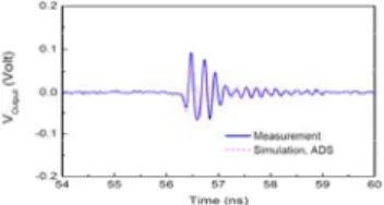
Fig. 3 Generated monocycle pulses of the proposed circuit scheme. (a) Simulation. (b) Measurement.
0 2 4 6 8 10
-80 -60 -40 -20 0
Normalized Spectrum (dB)
Frequency (GHz) Simulation Measurement
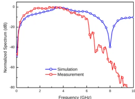
Fig. 4 Simulated and measured normalized pulse spectrum of the proposed monocycle pulse generator.
used in this work are MSS50-048-E25 and MMD-0840 from Metelics Cooperation. Optimized lengths of the four stubs are illustrated in Fig. 1 and all connection transmission lines are 10mm.
The external input source was a 10MHz square wave by an Agilent 33250A arbitrary waveform generator. The peak-to-peak voltage of the square wave is 5 V and the rise time is 5 ns. The measurement was taken by an Agilent DSO 54855A digital oscilloscope with a 20 GSa/s sample rate. The measurement result is shown in Fig. 3(b), which demonstrates a monocycle pulse with peak-to-peak voltage of 550 mV, pulsewidth of 320 ps, ringing level of as low as -22dB and good pulse symmetry.
The somewhat discrepancy between the simulated and measured results can be attributed to the inaccurate diode modeling in the simulation as well as to the bandwidth limitation of the digital oscilloscope in the measurement. The simulated and measured normalized pulse spectrum is shown in Fig.
4. As shown in the figure, the measured spectrum is centered at 3.6 GHz with a -10 dB bandwidth of 5.5GHz.
B. New design of slotted ground structure [3]
Figure 5(a) illustrates the geometry of a unit cell of the proposed meandered V-sickle slotted ground structure. By meandering the resonant V-shaped slotline in [4], the occupied size of the slotted ground structure can be substantially reduced. Similar to a conventional slotted ground structure, the proposed design can be roughly equivalent to a parallel RLC resonator which is in series with the microstrip line.
The element values of the equivalent circuit can be readily extracted by the formula in [5]. In designing the proposed slotted ground structure, the overall length of the etched slotline preliminarily determines the resonant frequency of the rejection band, and the flared angle θ under the microstrip line can be used to control the slope parameter of the resonator introduced. Accordingly, by tuning the parameters La, Lb and θ, the responses of the meandered V-sickle slotted ground structure can be readily controlled.
The slot width, Ws, on the contrary, is kept small to avoid potential parasitic radiation.
Figure 5(b) illustrates the proposed third-order bandstop filter by incorporating three cascaded meandered V-sickle slotted ground structure under the microstrip line. The initial design follows the standard filter theory [6] in order to meet the design requirements, and the slope parameters of the resonators used are (b1/Y0) = (b3/Y0) = 5.3094 and (b2/Y0) = 4.7736. However, owing to the fabrication limitation, it is then noted that the highest slope parameter attainable in this work is around 4.2 with the flared angle between the slots being 4 degrees. To tackle this problem, in our design the slope parameters of the resonators used are chosen to be 3.667 and 2.75, or equivalently θ1 = θ3 = 6° and θ2 = 10 °, respectively. Instead of setting the distance
between the resonators equal to one-quarter wavelength, in the design the distance Ld1 and Ld2 are fine-tuned to compensate the nonideal effects introduced by the resonators used.
The proposed design was fabricated on a 0.8-mm FR-4 substrate with a dielectric constant of 4.4 and loss tangent of 0.022. The dimension of the bandstop filter was optimized using the Ansoft HFSS 9.2 and the final dimensions are given by L1 = L3 = 5.2 mm, L2 = L4 = 4.4 mm, L5 = 4 mm, L6 = 2.8 mm, Ws = 0.2 mm, Ld1 = 4.6 mm, and Ld2 = 4 mm. The overall circuit size is 28 × 20 mm2. The characteristic impedance of the microstrip line is 50 ohms. It is interesting to note that the distances between the resonators are much shorter than one-quarter wavelength, which is likely a result of the slow wave behavior introduced by the meandered V-sickle slotted ground structure. The simulated and measured S-parameters of the proposed third-order bandstop filter are shown in Fig. 6. The measurement was performed by an Agilent E8362B performance network analyzer. Good agreement between the results can be readily observed. The signal suppression level is greater than 20 dB from 5.1 to 5.9 GHz, and can be as high as 40 dB at 5.5 GHz. At
(a) (b)
Fig. 5 (a) A unit cell of the proposed meandered V-sickle slotted ground structure. (b) Geometry of the proposed third-order bandstop filter.
Fig. 6 Comparisons of the simulated and measured S-parameters of the proposed bandstop filter.
(a) (b)
Fig. 7 (a) Circuit schematic diagram and (b) simulated and measured output waveforms of the three-derivative Gaussian pulse generator
the center frequency of the rejection band, on the other hand, the insertion loss is less than 2 dB.
Figure 7(a) illustrates the schematic diagram of the third-derivative Gaussian pulse generator used in this work. The pulse generator is composed of a shunt-mode SRD pulse generator and a differentiating circuit. The differentiating circuit also acts as resistive loadings to eliminate the late-time ringing of the output waveform. The shunt-mode pulse generator consists of a series inductor L1, a series resistor R1 and a shunt-to-ground step recovery diode D1. An external square-wave generator conducts the diode during the positive half cycle of the input signal. At the falling edge of the square wave, the diode initially remains turned on due to its uniquely long storage time. As the minority carriers are completely excluded, the diode turns off abruptly and the magnetic field energy stored in the inductor L1 is dissipates by means of an impulse current flowing through R1. It therefore results in a subnanosecond Gaussian pulse. The Gaussian pulse then enters into the differentiating circuit which is composed of three resistive loaded shunt stubs and two series lumped capacitors C1 and C2. The waveform at the output of the differentiating circuit is quite similar to the third derivative of a Gaussian impulse.
The proposed pulse generator was simulated using Agilent ADS 2006A, and fabricated on a 0.8-mm FR4 substrate. The SRD applied is a SMMD-0832 diode from the Metelics Cooperation®.
The optimized parameters are given by L1 = 1.5 nH, R1 = 180 Ω, R2 = R3 = 12 Ω, R4 = 10 Ω, C1 = 0.5 pF, and C2 = 1 pF. The microstrip lines in the stubs are chosen to be 50 ohms for matching purpose, and the lengths of the stubs are 1 mm. In the measurement the external excitation is provided by an Agilent 33220A arbitrary waveform generator with a 10 MHz 10-Vpp square wave. The rise and fall times are both 5 ns. The simulated and measured pulses at the output of the differentiating circuit are shown in Fig.
7(b). The measurement was performed by an Agilent digital oscilloscope DSO 81204B. The results further sustain the above discussions, and the output waveform has a peak-to-peak voltage of 430 mV and pulse width of 440 ps.
Combining the pulse generator in Section III and the bandstop filter in Section II, in this section a novel ultrawideband pulse shaper is proposed, and a photograph of the design is shown in Fig. 8. The overall size of the proposed pulse shaper is 47 × 20 mm2. In the simulation the responses of the bandstop filter were first simulated by the Agilent Momentum 2006 and then imported into the ADS 2006 to perform the transient analysis along with the pulse generator. The measurements were performed by both the Agilent 81204B digital oscilloscope and E4445A spectrum analyzer. Figure 9 illustrates the simulated and measured pulses at the output of the pulse shaper. Reasonable agreement between the
results can be observed and the discrepancy can be mostly attributed to the difficulty in accurately modeling the SRD used in the circuit. Referring to the figure, the measured pulsewidth is 1 ns and the peak-to-peak amplitude is approximately 160 mV.
Figure 10 compares the measured power density spectra at the outputs of the third-derivative Gaussian pulse generator and the pulse shaper, respectively. As shown in the figure, the power density spectrum of the output pulse is complied with FCC emission mask, and the rejection level is nearly 35 dB at the 5-GHz WLAN band.
C. New design of folded-strip UWB antenna [7]
The configuration of the proposed antenna is shown in Fig. 11. The antenna was fabricated on a 1.6-mm FR4 epoxy substrate with dielectric constant εr = 4.4 and loss tangent tanδ = 0.022. As shown in the figure, a forked-shape radiator is fed by a 50Ω microstrip line of length L3. The included angle α between the radiator and the ground plane primarily determines the in-band impedance matching and is given by
(a)
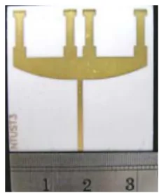
(b) Fig. 8 Photograph of the proposed ultrawideband pulse shaper. (a) Top view. (b) Bottom view.
Fig. 9 Simulated and measured output waveforms of the pulse shaper.
Fig. 10 Comparison of the measured power density spectra at the outputs of the three-derivative Gaussian pulse generator and the pulse shaper.
1 2 2
tan (L )
α= − W . (1)
In designing the antenna, the lowest operating frequency fl can be empirically approximated by
( ) L 4
l
l e ff l
e ff
c c
f ≈ ε λ ≈ ε
⋅ ⋅
(2)
2 2
2 2 1 s
Ll= L +W +(L −W ) (3)
1 2
r eff
ε =ε + , (4)
where Ll is the estimated longest current path along the outer edges of the radiating strips, and c and εeff
are the speed of light and the approximated effective dielectric constant, respectively. The highest antenna operating frequency, on the other hand, is principally determined by the distortion of radiation patterns. It is also worthwhile mentioning that according to the simulated current distributions, the current on the metal plate of a square monopole is in essence concentrated along the outer edges of the radiating plate. As a result, the interior metal has minor effects on the antenna performance and can be removed for design purpose.
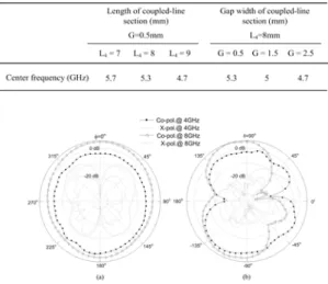
To achieve the required band-notched filtering property, the forked-shape strips are folded back to form a pair of coupled lines. By simply adjusting the length L4 and gap width G of the coupled-line sections, an additional resonance with desired band-rejected properties can be introduced to the antenna response. It should be emphasized that here the coupled lines neither support TEM mode nor form coupled microstrip lines since the lines are operated in inhomogeneous media without back ground plane. It complicates the analysis and the simplified equivalent circuit model will be discussed in Section III. The final design parameters are W1= 4.5 mm, W2= 5.8 mm, W3= 11 mm, Wm= 3.4 mm, Ws= 2 mm, L1= 12.5 mm, L2= 2 mm, L3= 11.5 mm, L4= 8 mm, L5= 2 mm, and G= 0.5 mm. The proposed antenna has an overall size of 30 by 30 mm2.
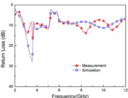
The simulated and measured return losses are shown in Fig. 12. The simulation was performed using Ansoft HFSS 9.2 while the measurement was taken by an Agilent E8362B performance network analyzer. The agreement between the simulation and measurement is fairly good except near the lower band edge. This discrepancy is believed to be caused by the interference of the connector and feeding cable in the measurement. The simulation result of the antenna without the folded strips, i.e. L4 = G = 0, is also shown in Fig. 12. From the figure it is evident that the desired filtering property is introduced by the folded strips as expected. Table I summarizes the simulation results regarding the center frequencies of the rejection band for several values of L4 and G. It is noted from the table that the notched frequencies move downward to the lower frequency range as L4
lengthens or G widens. The in-band impedance
matching, although not shown here for simplicity, remains roughly the same for both cases. In addition, it is also noted that the lowest antenna operating frequency decreases slightly as L4 increases. It can be readily accounted for by equations (2)-(4). The bandwidth controllability of the proposed band-rejected UWB antenna is another issue of interest. As shown in Fig. 12, the return loss of the antenna with folded strips reveals somewhat degradation in the frequency range of 4 to 5 GHz. It is likely a result of the slow roll-off rate (or poor frequency selectivity) of the band-notched resonator loaded to the antenna. To the best of author's knowledge, the bandwidth controllability of most recently proposed band-notched UWB antennas is relatively limited. It is owing to the fact that in such design only a single pair of resonators is loaded to the antenna structure. Accordingly, the notched bandwidth of a UWB antenna is simply inversely proportional to the quality factor of the resonator,
Fig. 11 The proposed antenna configuration.
Fig. 12 Simulated and measured return losses.
Fig. 13 Measured radiation patterns at 4 and 8 GHz. (a) xy-plane.
(b) xz-plane.
Fig. 14 (a) Schematic diagram of the coupled lines. (b) Circuit layout for extracting the lumped equivalent circuit model in (c). (c) Lumped equivalent circuit model of the coupled-line section. (d) Equivalent circuit model of the proposed antenna.
(a) (b)
Fig. 15 Comparisons of the input impedance of the one-port network in Fig. 4(b) to that of the lumped equivalent circuit model in Fig.
4(c). (a) Resistance and (b) Reactance
(a) (b)
Fig. 16 Comparisons between the simulated input admittance of the proposed antenna by HFSS and by the equivalent circuit model in Fig. 4(d). (a) Conductance. (b) Susceptance.
and has limited tunability if one also wants to keep the center frequency of rejection band unchanged. It is, in essence, similar to the case of a first-order microwave bandstop filter.
The antenna radiation patterns were measured in a 7×3.2×3 m3 anechoic chamber in NTUST. The measurement was performed by an Agilent E8362B network analyzer along with NSI 2000 far-field measurement software. In the measurement the connecting cables were carefully shielded by absorbers to reduce the multiple-reflection interference. Figure 13(a) and (b) illustrates the measured radiation patterns in the xy- and xz- planes at the center frequencies, 4 and 8 GHz, of the UWB low and high bands. Here the UWB low band is referred to as the mandatory band from 3.1 to 5.1 GHz whereas the UWB high band stands for the optional band from 5.85 to 10.6 GHz. The frequency band from 5.1 to 5.85 GHz, on the other hand, is not used in modern UWB systems due to the potential interference problem. The patterns in the xy-plane are quite omnidirectional as expected whereas in the xz-plane the radiation patterns remain roughly a dumbbell shape over the frequency band of interest.
The cross-polarization levels are generally much lower than the co-polarization ones. The effect of antenna ground plane is also studied since its size is comparable to the radiator and contributes to the radiation. The ground plane size in the original design, i.e. L3 by W, is 11.5 by 30 mm2. It is observed through HFSS simulation that as L3 varies from 11.5 mm to 26.5 mm, the antenna input matching at the UWB mandatory band experiences somewhat degradations whereas the return loss at the optional band remains better than 10 dB. The ground plane width W, on the other hand, is found to have limited effects on the antenna matching when varying from 30 mm to 45 mm. The shapes of radiation patterns remain principally unchanged despite the variations in the antenna ground plane.
Nevertheless, it is indeed noted that the dumbbell-shaped pattern in the xz-plane tilts gradually as L3 lengthens. Further discussion on the frequency dependence of the antenna radiation characteristics will be addressed in Section IV with the help of normalized antenna transfer functions.
A lumped equivalent circuit model is discussed for the proposed antenna. Conceptually, the coupled-line section in the forked-shape radiator can be represented by the schematic diagram in Fig. 14(a).
In the figure Zoe and γe are the even-mode characteristic impedance and complex propagation constant, respectively, of the coupled lines and Zoo
and γo are the corresponding odd-mode parameters.
For correct modeling of the folded strip, the coupled lines in Fig. 14(a) are connected at one end and open-circuited in one of the two lines at the other end.
The input impedance of the resultant one-port network can be readily expressed by [8]
,
1( tanh - coth )
in CL 2 oo o oe e
Z = Z γ l Z γ l . (5)
It is evident from (5) that as the length of the coupled lines approximating one-quarter wavelength long, it behaves like a parallel resonator which gives rise to the band-notched filtering property at the targeted rejection band.
However, the antenna modeling using the schematic diagram in Fig. 14(a) is not as straightforward as expected owing to the difficulties in accurately estimating the radiation loss of the coupled lines in the forked-shape radiator. To tackle this problem, in this paper we attempt to first deal
(a) (b)
Fig. 17 A modification of the antenna in [10]. (a) Antenna configuration. (b) Equivalent circuit model.
(a) (b)
Fig. 18 Proposed antenna configuration. (a) Oblique view.
(b) Top view.
Fig. 19 Equivalent circuit model of the proposed antenna.
Fig. 20 Photograph of the proposed antenna with the one-port network in Fig. 14(b) which
consists of a coupled-line section and a finite-size ground plane. Here the dimensions of the coupled lines and ground plane are the same as those of the proposed antenna, and a delta source is served as the excitation. By means of full-wave simulation, the network parameters of this one-port network can be easily achieved and transformed into the lumped equivalent parallel resonant circuit in Fig. 14(c) with
2 1 1
o
f f
FBW f Q
= − =
, (6)
eq eq
o
L R ωQ
= , (7)
2
1
eq
o eq
C =ω L
. (8) Here FBW represents the fractional bandwidth with
the magnitude of the input impedance dropping to 0.707 of its peak value, Q is the quality factor, and ω0 is the center angular frequency. The calculated element values of the lumped circuit model using (6)-(8) are summarized in Table II. Noted that Req
corresponds to the real part of the input impedance at the center frequency ω0. Figure 15 compares the input impedance of the one-port network in Fig. 14(b) to that of the equivalent circuit in Fig. 14(c). Fairly good agreement can be observed over the frequency band of interest.
With the lumped equivalent model in Fig 14(c), we further note that the proposed antenna can be modeled by an equivalent circuit in Fig. 14(d). Here the two lossy parallel resonators represent the pair of folded strips in the fork-shaped radiator. The flared metal plate between the folded strips and the feeding microstrip line behaves quite similar to a quarter-wavelength transformer, and can be therefore modeled as a pair of J-inverters. The J-inverter is cascaded with the parallel resonator and transforms it into a series one at the antenna feeding point. The value of the J-inverter is determined by equaling the admittance levels of the antenna and the equivalent circuit model, and is given by 0.0154 mho (i.e. 65 ohm). The conductance Grad represents the antenna radiation conductance, and is selected to be 0.02mho (i.e. 50 ohm) to account for the wideband nature of the antenna. The input admittance of the antenna equivalent circuit is hence given by
2 ,
, in ant rad 2
in eq
Y G J
= + Y , (9)
2 0
, (1 2)
in eq eq eq
Y G j Cω ω
= + −ω . (10)
Figure 16 compares the antenna input admittance simulated by HFSS to that calculated using (9). In the full-wave simulation the antenna response has been de-embedded to the feeding point in advance.
Referring to the figure, the trends of curves agree reasonably well over the operating frequencies, and both responses behave like series resonators at the targeted notched frequency band. The discrepancy
between the curves can be mostly attributed to the inaccurate modeling of the coupled-line sections on the radiator. That is, the one-port network in Fig.
14(b) is still too lossy to accurately model the coupled lines in the fork-shaped radiator. It in turn results in an equivalent circuit with lower-Q and wider rejection bandwidth than the actual one.
Despite the error in the equivalent circuit model, the results still provide valuable information of the antenna behavior and sustain the correctness of the proposed equivalent circuit model.
D. Multi-resonator loaded band-notched UWB antenna [9]
The design initially begins with the antenna shown in Fig. 17(a), which is a minor modification of the antenna discussed in [10]. The behavior of the antenna in Fig. 17(a) is quite similar to that of the
Fig. 21 Simulated and measured return losses of the proposed antenna.
(a) (b)
Fig. 22 Measured radiation patterns in the yz-plane at (a) 4 GHz and (b) 8 GHz.
(a) (b)
Fig. 23 Measured radiation patterns in the yz-plane at (a) 4 GHz and (b) 8 GHz.
(a) (b)
Fig.24 Measured gain responses of the proposed antenna at (a)θ=0 , 90 , 180 , -90o o o o (b)θ=45 , 135 , -135 , -45o o o o.
antenna proposed in [7], and can be represented by the same equivalent circuit model in Fig. 17(b). In the circuit model the pair of folded strips in the fork-shaped radiator can be represented by two lumped parallel lossy RLC resonators. The flared metal plate between the folded strips and the microstrip feed line behaves similar to a quarter-wavelength transformer, and can be modeled as a pair of J-inverters. The wideband nature of the antenna, on the other hand, can be readily accounted for by a constant radiation conductance Grad in the model with Grad = 0.02 mho. If necessary, the procedure discussed in [7] can be used to extract the element values of the lumped circuit model in Fig. 17 (b) as well.
To explore the concept of multi-resonator loaded band-notched ultrawideband antenna, in this paper we discuss a new antenna design by introducing an extra pair of folded strips to the antenna in Fig. 17 (a).
The antenna configuration is illustrated in Fig. 18. As shown in the figure, the new design lies in the xy-plane with its normal direction parallel to the z axis. The antenna is symmetric about its centerline, and consists of a microstrip feed line, a truncated ground plane, a flared metal plate, and two pairs of the folded strips. It can be shown that the folded strip behaves like a parallel LC tank [7], and can be physically realized by connecting the top and bottom metal foils by rows of via holes. The radius of the via hole is 0.2 mm. The coupling between the metal foils provides the necessary capacitive loading whereas the strip itself contributes to the inductance value of the resonator. For the sake of simplicity, in the following discussions the two pairs of resonators are referred to as the exterior and the interior resonators, and the subscripts “e” and “i” are used to distinguish the parameters associated with the exterior and interior resonators, respectively.
To explain the complex behavior of the antenna, here an equivalent circuit model is illustrated in Fig.
19. In the discussion in this paragraph the subscripts are neglected for the sake of brevity. Referring to the circuit model, each folded strip can be represented by a lumped parallel lossy RLC resonator. The resonance frequency of the resonator can be readily controlled by adjusting the equivalent inductance and capacitance values, i.e. Leq and Ceq, of the resonator, which are in turn determined by the geometric parameters of the folded strip. As shown in Fig. 18, the area of the metal plate on the bottom layer, i.e.
Lcap × Wcap, preliminary determines the value of the capacitive loading. On the other hand, the insets on the radiating strip on the top layer principally act as the inductive loading, and have the ability to fine-tune the inductance value of the resonator. It should be aware that as the areas of the insets (Lind by Wind) become larger, the capacitive loading of the
resonator will decrease accordingly. It implies that there exists a nonlinear dependence between the areas of the inductive insets and the resonance frequency of the resonator. The equivalent resistance Req, meanwhile, accounts for the conduction loss, the dielectric loss, as well as the parasitic radiation loss of the folded strip, and can be used to determine the quality factor of the resonator.
In the meantime, as shown in Fig. 18, the tapered profile of the flared metal plate between the interior and exterior folded strips is described by an equation
of an arc. Similar to the antenna in [7], it behaves like a quarter-wavelength impedance transformer. In the equivalent circuit model, a pair of J-inverters, J1,2
and J3,4, are adapted to characterize the transformer behavior of the flared metal plate. The parasitic coupling between the interior and exterior resonators also contributes to the inverters as well. On the other hand, the cross coupling between the pair of interior resonators, which are in close proximity to each other, can be modeled by an additional J-inverter J2,3, and the coupling coefficient can be calculated using the standard coupled resonator circuit theory in [6].
Finally, the radiation conductance Grad is again used to account for the wideband nature of the proposed design, and the microstrip feed line can be represented by a transmission line with a characteristic impedance Z0 and propagation constant β.
Following the discussions, the antenna was first optimized by the full wave simulation solver HFSS version 9.2, and then fabricated on a 20-mil Rogers 4003 substrate with a dielectric constant of 3.38 and loss tangent of 0.0027. A photograph of the fabricated antenna is shown in Fig. 20. The overall dimension of the antenna is 34 by 34 mm2. The truncated ground plane occupies an area of 16.5 by 34 mm2. It is noted that the truncated ground plane, whose size is comparable to the radiator, has significant effects on the antenna performance and also contributes to the radiation.
First of all, the antenna performances in terms of the return loss, radiation patterns, and gain responses versus frequencies are investigated in this subsection.
The simulated and measured antenna return losses are illustrated in Fig. 21. Owing to the strong reactive near field of the proposed multi-resonator loaded antenna, it is observed through measurement that the antenna return loss is very sensitive to the SMA connecter attached as well as to the truncated ground plane used. To tackle this problem and to improve the measuring accuracy, in this work the antenna return losses were measured with the help of a Cascade Microtech MTF26 microstrip test fixture along with an Agilent PNA-L 5230A at National Taiwan University. Several absorbers were placed around the test fixture to minimize the undesired coupling. Referring to Fig. 21, reasonable agreement between the simulated and measured return losses can be readily observed in the frequency band of concern, and the discrepancy is likely a result of the parasitic coupling between the antenna and the near-by metallic objects. In addition, the rejection band at the 5-GHz WLAN radios demonstrates two resonance peaks, which are at 5.35 and 5.75 GHz, respectively. The maximum signal rejection levels from the measured results are 3.61 and 3.97 dB. The simulated signal rejection levels, on the other hand, are slightly higher than the measured ones, which can be accounted for by the parasitic coupling that does
not take into account in the simulation. It is also worthwhile to mention that the roll-off rate of the antenna return loss at the notched frequencies is significantly faster than that of a conventional single resonator loaded ultrawideband antenna. As a result, the measured return loss preliminarily sustains the design concept discussed in the previous section.
The antenna radiation patterns were measured in a 7×3.2×3 m3 anechoic chamber at National Taiwan University of Science and Technology. The measurement was performed by an Agilent E8362B network analyzer along with NSI 2000 far-field measurement software. In the measurement the connecting cable was carefully shielded by absorbers to reduce the multiple-reflection interference. In addition, to minimize the parasitic coupling the antenna was fed directly from the connecting cable without a SMA adapter. The simulated and measured radiation patterns in the yz- (H-) and xz- (E-) planes at the center frequencies, 4 and 8 GHz, of the UWB low and high bands are illustrated in Figs. 22 and 23, respectively. Here the UWB low band is referred to as the mandatory band from 3.1 to 5.1 GHz whereas the UWB high band stands for the optional band from 5.85 to 10.6 GHz. The agreement between the simulated and measured radiation patterns is very excellent in the yz-plane and remains acceptable in the xz-plane. The discrepancy in the xz-plane can be mostly attributed to the interference of the bended coaxial cable used for feeding purpose in the measuring arrangement, as illustrated in the inset of Fig. 23. Referring to the figures, the radiation pattern in the yz-plane is nearly omnidirectional at the UWB low band, and becomes similar to the shape of a four-leaved clover as the operating frequency increases. On the contrary, the radiation patterns in the xz-plane remain roughly a dumbbell-like shape over the frequency band of interest. The cross-polarization level is generally much lower than the co-polarization one in the low frequency range, and rises considerably with the increase of the operating frequency. It, nevertheless, remains acceptable except at the upper edge of the UWB high band.
The antenna was further examined by means of the gain responses versus frequencies from 3 to 11 GHz.
Figure 24(a) illustrates the measured gain responses in the yz-plane at θ=0 , 90 , 180 , and -90o o o o , whereas the gain responses in the same plane as
o o
45 , 135 ,
θ= -135 , and -45 are unveiled in o o Fig. 24(b). The required masked spectrum at the WLAN radios is also depicted in the figures for comparison purpose. As shown in the figures, the gain responses fluctuate back and forth between 0 to 2 dBi at the UWB low band, and may climb up to 5 dBi at the UWB high band in the azimuth plane, i.e. θ= ± 90o. In addition, a rejection band with good frequency selectivity can be readily observed at the 5-GHz WLAN band with two notch peaks. At
Fig. 10 The simulated and measure return losses of the antenna design for compensating the effects of the ground plane with WGND = 44 mm.
90θ= o the gain suppression at the center frequency of the rejection band can be more than 20 dB. Moreover, owing to the slight shifts in the center frequencies of the notch peaks with respect to the reception angle, the rejection band may split into two individual ones at certain directions, e.g. 135θ= o. Nevertheless, the band-notched phenomenon still remains acceptable in most of the reception directions. Further investigation with the help of the multilayered printed circuit broad fabrication process is currently under investigation to mitigate the spatial dependence of the gain responses at the notched frequencies. The result will be discussed in a future publication. Despite the spatial dependence of the rejection band, the experimental results manifest that the proposed design demonstrates bandstop-filter-like response with good frequency selectivity at the targeted rejection band.
Finally, I t has been mentioned that the proposed antenna is very sensitive to the truncated ground plane used in the design. Accordingly, it is necessary to discuss the effects of the ground plane in greater detail. With the help of the full-wave simulation solver HFSS, we observe that the behavior of the rejection band can be dramatically affected by the variations of the truncated ground plane. For demonstration purpose here an example is illustrated in this subsection with the width of the ground plane WGND being widened by 10 mm. It is observed through simulation that as the ground plane size becomes larger the notch peaks may be further apart and tend to split into two individual rejection bands.
To tackle this problem, the antenna parameters for bandwidth controllability in Section III.B can be applied to fine-tune the antenna response. By relocating the exterior pair of folded strips with a distance of Wg,e = 12.8 mm, well-behaved band-notched response with good frequency selectivity at the WLAN band can be readily restored.
The simulated and measure return losses of the re-tuned antenna design are depicted in Fig. 25.
Fairly good agreement between the results can be again observed. Meanwhile, it is also noted from the
figure that the impedance matching at the UWB high band can be substantially improved as the size of the ground plane becomes larger. With this illustration, we can therefore conclude that the nonideal effects of the antenna ground plane on the desired rejection characteristics can be simply compensated by applying the tuning parameters discussed in previous subsection.
III. 總結
本計畫於執行期間內,成功完成新型脈衝產生器、
缺陷接地結構、帶拒濾波器、超寬頻塑波器、折疊 型超寬頻天線、多重共振器負載超寬頻天線等等設 計,目前獲得刊登之SCI論文共兩篇,另有兩篇SCI 期刊論文在審查中。此外,本計畫亦完成了新型微 波取樣器的設計與驗證,但因為申請專利之議題,
目前暫無法公開說明。總體論述,本計畫之研究成 果頗為豐富,對於第一次執行國科會研究計畫的申 請人,無異是一大鼓舞,億期待未來繼續努力精 進!
參考文獻
[1] J. Han and C. Nguyen, A new ultra-wideband, ultra-short monocycle pulse generator with reduced ringing, IEEE Microwave and Wireless Component Letter 12 (2002), 206-208.
[2] T. G. Ma*, C. J. Wu, P. K. Cheng, and C. F. Chou, “An ultrawideband monocycle pulse generator with dual resistive loaded stunt stubs,” Microw. Optical Technology. Lett., vol.
49, no.2, pp. 459-462, Fed. 2007.
[3] C. F. Chou and T. G. Ma*, “A meandered V-sickle slotted ground structure and its applications to ultrawideband pulse shaper,” IEEE Microv. wireless Compon. Lett., submitted for publication.
[4] D. J. Woo, T. K. Lee, J. W. Lee, C. S. Pyo, W. K. Choi,
“Novel U-slot and V-slot DGSs for bandstop filter with improved Q factor,” IEEE Trans. Microw. Theory Tech., vol.
54, pp. 2840-2847, June 2006.
[5] D.J. Woo, T.K. Lee, “Suppression of harmonics in Wilkinson power divider using dual-band rejection by asymmetric DGS,” IEEE Trans. Microw. Theory Tech., vol. 53 , pp.
2139-2144, June 2005.
[6] J. S. Hong, M. J. Lancaster, Microstrip Filters for RF/Microwave Application, John Wiley & Sons, Inc., 2001.
[7] T. G. Ma* and S. J. Wu, “Ultrawideband band-notched folded strip monopole antenna,” IEEE Trans. Antennas Propagat., vol. 55, pp. 2473-2479, Sep. 2007.
[8] G. L. Matthaei, L. Young, E. M. T. Jones, Microwave Filters, Impedance-matching networks, and Coupling Structure, Artech House, 1980.
[9] T. G. Ma*, R. C. Hua and C. F. Chou, "Design of a multi-resonator loaded band-rejected ultrawideband planar monopole antenna with controllable notched bandwidth,"
IEEE trans. Antennas Propagat., submitted for publication.
[10] T. G. Ma* and S. J. Wu, “A new band-notched U-shape folded monopole for UWB applications,” in 2006 IEEE AP-S Int.
Symp. Dig., Albuquerque, NM, July 2006, pp. 1643-1646.
行政院國家科學委員會補助國內專家學者出席國際學術 會議報告
96 年 6 月 30 日 計畫編號 NSC 95-2221-E-011-021
計畫名稱 應用超寬頻技術之無線感測網路射頻前端元件之研究 – 使用缺陷接地結 構
出國人員姓名 服務機關及職稱
馬自莊
國立台灣科技大學 電機工程系 助理教授 會議時間地點 1) 2007.06.03~2007.06.08 (IMS)
2) 2007.06.10~2007.06.15 (APS)
會議名稱
國際電機電子工程師學會(IEEE)所舉辦之
1) 2007 國際微波年會(International Microwave Symposium, 6/3~6/8) 2) 2007 天線與電波傳播國際研討會(2007 International Symposium on Antennas and Propagation, 6/10~6/15)
發表論文題目
1) IMS:
C. W. Wang, T.-G. Ma* and C. F. Yang, “Miniaturized branch-line coupler with harmonic suppression for RFID applications using artificial transmission lines.”
2) APS:
W.-H. Wang, K.-C. Liao, H.-W. Liu, S.-F. Yang, C.-F. Yang*, T.-G. Ma, N.
Tai, “A metal mounting tag for passive UHF RFID applications.”
R. C. Hua*, C. W. Wang, and T.-G. Ma, “A planar quasi-Yagi antenna with a new microstrip-to-CPS balun by artificial transmission lines.”
一、參加會議經過
首先感謝 貴會的出國差旅費補助,俾使敝人在經濟壓力負擔較輕的前提下,連續 參與本年度由 IEEE Microwave Theory and Techniques 學會所主辦、每年度國際上最大型 微波研討會 - 2007 國際微波年會(International Microwave Symposium, IMS),以及由 IEEE Antennas and Propagation 學會所主辦,每年度國際上最大型天線與傳播研討會 (2007 International Symposium on Antennas and Propagation, APS)。本年度最令人津津樂道 的莫過於這是電磁波領域兩大會議首度假同一地點舉辦(夏威夷),且 AP-S 還特地將會 議時間由以往的七月中上旬,提前至六月中旬,俾使與會者可以同時參與兩項盛會,聆 聽整個電波領域最新的發展趨勢及技術成就,實屬百年難得一見之機會。
因此機緣難得,敝人自去(95)年暑假開始即著手與研究所同學兢兢業業,積極進行 研究工作,終於順利將論文即時完成,並分別投稿之 IMS 及 APS 會議,獲得接受。其中 IMS 會議之接受率僅 45~50%左右,扣除海報張貼及十分鐘口頭報告的短論文,能夠獲得 二十分鐘口頭報告時間的論文僅 25%左右。此次敝人與楊成發教授所共同指導之碩士班 學生王釗偉所投稿的論文:『Miniaturized branch-line coupler with harmonic suppression for RFID applications using artificial transmission lines』,因具有獨特之創見,獲得 IMS 會議之 20 分鐘口頭報告之機會,實屬不易。至於 APS 會議方面,敝人今年亦有兩篇論文發表,
並獲邀擔任壁報議程 Session IF 208 之主席。
懷著能夠連續聆聽國際最頂尖之微波及天線傳播會議的興奮心情,以及對夏威夷熱 帶島國的美好憧憬,敝人與王釗偉同學於 6/3 下午搭乘華航班機飛往檀香山,歷時十個 小時抵達,同班機遇到許多微波領域的前輩老師如陳俊雄老師、王暉老師、呂學士老師、
孟慶宗老師、黃天偉老師等等,難得微波領域的研究學者共聚一堂。夏威夷當地時間與 台灣之時差為 18 小時,因此抵達時間為清晨 6:00 左右。由於無法立即進入下榻旅社,
華航與旅行社貼心的為我們設計了半日的 city tour,先後參觀珍珠港及檀香山市區,為此 趟夏威夷學習之旅拉開序幕,直到下午三點方住進旅社。
次日為夏威夷時間六月四日,當日為 IMS 會議所安排之子會議 RFIC 會議的全日議 程,RFIC 目前雖不尚是敝人的研究領域,但一直是自我期許邁向的研究方向,也是時代 之潮流所趨,因此能夠參與此一會議,對自我的成長有相當的意義。敝人與隨行之王釗 偉 同 學 共 參 加 RM01B: Pulsed UWB transceiver, RM03D transmitter linearization techniques 以及 RM04A: RFID 等議程,並抽空前往展覽會場參觀。由於商業展覽傳統上 一直是 IMS 會議中相當重要的一環,透過與展覽廠商的交流,除了可以瞭解目前市場上 產品研發、儀器設備、元件更迭的最新狀況,亦可獲得許多寶貴的資訊。此次我們除對 於量測設備的廠商如 Agilent, Tektronix, Anritsu 以及模擬軟體如 Ansoft, IE3D 等持續關注 外,另外也肩負著尋找與永奕科技所合作之 RFID 建教計畫所需的電路元件的任務。透 過不斷的詢問與交流,我們獲得了許多寶貴的資訊。當日晚間雖有 Microwave Journal 所 舉辦之 reception 活動,但身體卻已經敵不過時差的呼喚,早早回到旅館休息,並準備 次日下午的論文發表。
次日(週二)上午首先參加 IMS 的 plenary speech,該演講係介紹寬頻通訊的未來 趨勢,演講者皆為 Qualcomm 的副總裁,對於瞭解目前工業界最新的演進脈動有著相當 大的幫助。我們的演講安排在下午的議程:Session TU3B: Hybrids and Coupler I,由於這 次是王釗偉同學第一次出國報告論文,因此他格外緊張也格外慎重。此篇論文主要是講 述利用一種新型人造傳輸線進行微波電路縮小化實現的方式,該形式傳輸線的面積縮小