國立臺灣大學電機資訊學院電子工程學研究所 碩士論文
Graduate Institute of Electronics Engineering
College of Electrical Engineering and Computer Science National Taiwan University
Master Thesis
考慮電源供應雜訊之動態時序分析器
Power-Supply-Noise-Aware Dynamic Timing Analyzer
謝弘毅 Hung-Yi Hsieh
指導教授:李建模 博士 Advisor: Dr. Li, Chien-Mo
中華民國 103 年 9 月
September, 2014
i
ii
iii
致謝
經過這兩年多的研究生活,首先要謝謝我的父母,有時候很晚回家,他們犧牲 睡眠的等著我回家;有時候研究上不順利,他們也都承受著我的負面情緒,所以現 在終於畢業了,最感謝的就是他們,讓我能無後顧之憂的努力學業。接著要謝謝我 的指導教授,李建模教授,在研究上,老師扮演一個監督者,督促著進度並且讓我 很耐心地跟我們討論;在職前訓練上,老師扮演一個很好的教練,不辭辛勞地一遍 一遍糾正我的不足;在平時,老師十分關心大家的生活,體貼著大家的不方便。
接著要謝謝實驗室的博士班學長,首先是炳川學長,雖然跟學長只有幾面之緣,
但碩二時,包含商業軟體使用的問題以及計畫報告書的撰寫上,幫忙很多也很大。
再來是柏瑞學長,許多關於會議和計畫的問題還要是麻煩學長解答,而學長也總是 不厭其煩得回答我們,此外,也要謝謝學長花時間替我解決許多投影片與口試上的 問題。最後要謝謝官榆學長,許多程式與演算法上的問題,學長都能很細心的回答 並給我們很好的意見。對於我們上一屆的學長,也非常的感謝。謝謝瑋陞學長,畢 業前很熱心的跟我討論研究方向,畢業後還回來幫我修改口試頭影片。謝謝啟仁學 長,在國科會計畫上留給我很多資源可以參考,在電子電路上也像活字典般有問必 答。謝謝泓頤學長,在畢業前常推薦我很多很棒的電影,在畢業後也總是能在數學 推導上跟我討論。謝謝介智學長,在我考研究所時給我很多參考資料,也不厭其煩 的幫我解答許多疑問。謝謝聖章學長,在我當會計時幫忙很多,有任何問題都能告 訴我該怎麼做或是可以提供我查詢的管道。
iv
最要感謝的還是同一屆的各位同學。謝謝詩安,因為是同個大學的緣故,所以 一開始有問題總是會找你幫忙,做研究時也常找你討論,修課時也真的多虧了你,
我的研究生涯才能較為順利的過關。謝謝介甫,總是可以分擔我的怪,讓我不是實 驗室最怪的人,也謝謝你常用美聲療癒大家的心靈。謝謝士閔,總是很細心的跟我 們討論很多事情,並能提出很多不同的見解。謝謝昂鋒,總是寄信給大家提醒開會 的時間。
最後要謝謝下一屆的學弟們,他們不僅要幫學長做一些事情,還要準備眾多的 考試以及作業。其中最謝謝承佑學弟,在研究上幫助很多,幾乎可以說,沒有你就 沒有這個成果,希望你之後研究順順利利,祝你早點畢業。至於其他學弟,謝謝大 家的陪伴,帶給我許多歡笑。希望大家未來都能順順利利的完成學業,並進入理想 的公司。
v
摘要
當測試超大型積體電路晶片時,由於電壓降和電感電壓的影響,電源供應雜訊 會導致良率損失。在這篇論文中,我們提出一個考慮電源供應雜訊之動態時序分析 器。我們提出的分析器提供合理的準確度和比現存工具還快的速度。因為我們提出 的方法是基於線性函數而不是解非線性函數,所以是非常可調整的。實驗結果顯示:
在小電路中,與 HSPICE 相比的誤差小於 90%,而速度快約 288,000 倍;在大電路 中,我們達到比 NANOSIM 快八倍的速度,而誤差小於 50%。我們使用此分析器 在一個有一百萬個邏輯閘的測試電路上,並且從三萬一千個測試向量中辨別出 12366 個時序違規的測試向量,這是傳統方法很難找得到的。
關鍵字:電源供應雜訊、電壓降、電感電壓、電荷、動態時序分析器。
vi
Abstract
Due to the effect of IR-drop and Ldi/dt, power supply noise can cause yield loss when testing VLSI chips. In this thesis, we propose a power-supply-noise-aware dynamic timing analyzer, IDEA (IR-Drop-aware Efficient timing Analyzer). The proposed analyzer provides reasonable accuracy at much faster speed than existing tools.
This technique is very scalable because it is based on linear functions, instead of solving nonlinear functions. The experimental results show, for small circuits, the error is less than 90% and the runtime is about 288,000 times shorter compared with HSPICE. For large circuits, we achieved eight times speed up compared with NANOSIM with error less than 50%. IDEA identifies 12366 timing-violation test patterns (out of 31K test patterns) for a 1M gate benchmark circuit which are difficult to detect by traditional techniques.
Key Words: power supply noise, IR-drop, Ldi/dt, charge, dynamic timing analyzer.
vii
Table of Contents
1Chapter 1 Introduction ... 1
1.1 Motivation ... 1
1.2 Proposed Technique ... 3
1.3 Contributions ... 6
1.4 Organization ... 7
2Chapter 2 Background ... 8
2.1 PSN Estimation ... 8
2.2 Extra Gate Delay Calculation ... 12
2.3 PSN-Aware Timing Analysis ... 14
3Chapter 3 Proposed Techniques... 17
3.1 Overall Flow ... 17
3.2 Charge Model ... 19
3.3 Extra Gate Delay (Δd) Estimation ... 22
3.4 Window Partition ... 31
4Chapter 4 Experimental Results ... 33
4.1 Experimental Setup ... 33
4.2 IR-drop Only Experiments ... 34
4.3 IR-drop and Ldi/dt Experiments ... 40
4.4 Comparison of Dynamic and Static Window Partition ... 42
5Chapter 5 Discussion ... 44
5.1 False Hazard ... 44
5.2 Limitation of Multiple Clock Cycles ... 45
5.3 Interaction between Extra Gate Delay and Event Position ... 48
5.4 Impact of Different Current Model ... 52
6Chapter 6 Conclusion and Future Work ... 57
7References ... 59
viii
List of Figures
Figure 1.1 Comparison of extra delay ratio between 180nm and 45nm [Okumura 2010]
... 1
Figure 1.2 IR-drop maps (a) without package effects and (b) with package effects [Cadence 2009] ... 2
Figure 1.3 Concept of our approach ... 4
Figure 1.4 Overall flow of our proposed technique... 5
Figure 1.5 Histogram of path delay without PSN and with PSN (leon3mp) ... 6
Figure 2.1 Concept of multigrid ... 11
Figure 3.1 IDEA flow (for a single test pattern) ... 18
Figure 3.2 Example of power nodes and ground nodes ... 20
Figure 3.3 Average current for (a) output rising and (b) output falling ... 21
Figure 3.4 Example of rising gate delay estimation of gate 2 ... 22
Figure 3.5 Example of I/O waveform considering PSN ... 26
Figure 3.6 Current waveform transformation ... 29
Figure 3.7 Switching gate delay crosses a window boundary ... 31
Figure 4.1 VDD/GND power grid ... 33
Figure 4.2 Difference between drain current and peak current ... 38
Figure 4.3 Histogram of path delay (leon3mp) ... 40
Figure 4.4 Simple package model ... 40
Figure 4.5 Extra delay ratio falls with multiple clock cycles (leon3mp) ... 42
Figure 4.6 Extra path delay error of static window partition (b17) ... 43
Figure 5.1 Example of false hazard ... 44
Figure 5.2 Impact of LTE on V(th) (leon3mp) ... 47
Figure 5.3 IDEA flow with iteration ... 49
Figure 5.4 Change of extra path delay during twenty iterations (b17) ... 51
Figure 5.5 Rising gate delay estimation for an inverter ... 53
Figure 6.1 Neighboring logic gates near critical path [Enokimoto 2009] ... 58
ix
List of Tables
TABLE 2.1 Comparison of previous translation from PSN to extra gate delay... 14
TABLE 2.2 Comparison of previous PSN-aware timing analysis ... 16
TABLE 3.1 Average current cases ... 21
TABLE 4.1 Benchmark circuits ... 34
TABLE 4.2 Experimental results of path delay ... 36
TABLE 4.3 Experimental results of total path delay ... 37
TABLE 4.4 Experimental results of total path delay with package ... 41
TABLE 5.1 Runtime of iterations ... 51
1
1
Chapter 1 Introduction
1.1 Motivation
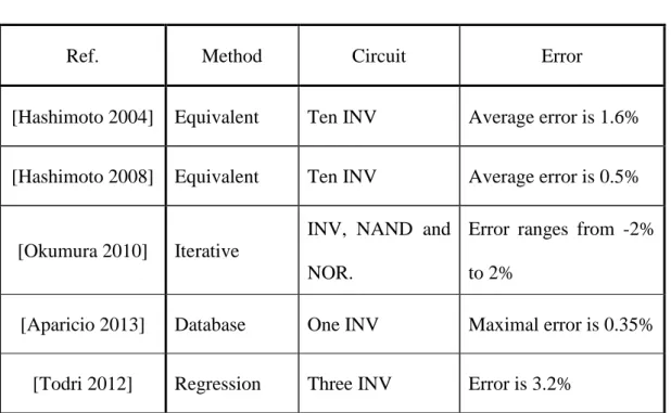
Power supply noise (PSN) becomes an important concern for VLSI system design and test [Shepard 1996][Saxena 2003][Wang 2005][Tehranipoor 2010]. PSN reduces the actual voltages supplied to logic gates, which also reduces signal integrity [Ma 2009].
Excessive PSN can degrade circuit performance by inducing extra gate delay, or even lead to timing failure of logic gates [Chen 1997][Jiang 1999]. It is also a well-known problem that excessive PSN during test can induce significant yield loss [Wang 2006][Li 2013]. Moreover, with technology scaling and power supply voltage lowering, path
delay becomes more sensitive to power supply voltage, as shown in Figure 1.1 [Okumura 2010]. X axis is PSN (ΔV) and Y axis is extra delay ratio, which is the ratio of extra path delay to path delay (ΔDpath/Dpath). Figure 1.1 shows extra delay ratio at 45nm is about five times bigger than at 180nm when ΔV=0.2V.
Figure 1.1 Comparison of extra delay ratio between 180nm and 45nm [Okumura 2010]
2
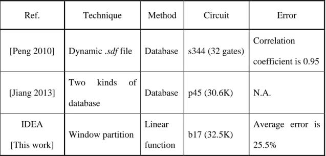
PSN can be classified into (1) IR-drop due to the parasitic resistances of on-chip interconnects, and (2) Ldi/dt due to package inductance. The first component (IR-drop) is a high-frequency noise, which is generated by switching gates. Traditional IR-drop analyzer shows the IR drop waveform or hot spot maps, but it is not clear how to translate IR-drop waveform to timing. The second component (Ldi/dt) is a mid-frequency noise, which is generated by off-chip inductance or package inductance [Ma 2011][Aparicio 2012]. Figure 1.2 compares IR-drop maps without package effects and with package effects. In Figure 1.2(a), the worst-case IR-drop without package effects is 147.5mV.
In Figure 1.2(b), the worst-case IR-drop with package effects is 179.3mV. It can be seen that the effects of package need to be considered since we may overestimate circuit performance by ignoring package effects.
(a) (b)
Figure 1.2 IR-drop maps (a) without package effects and (b) with package effects [Cadence 2009]
3
PSN-aware timing analysis can be classified into two classes. Static timing analysis does not require input patterns whereas dynamic timing analysis does. Static timing analysis is computationally efficient but it has problems to determine the value of PSN [Enami 2008]. Existing dynamic timing analysis tool is accurate but slow. For example, a commercial tool takes about twenty days to simulate all 31K test patterns for a million-gate benchmark circuit. Therefore, fast dynamic timing analysis for all test patterns is much needed to ensure both good test quality and low yield loss.
1.2 Proposed Technique
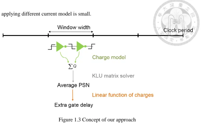
Figure 1.3 shows the concept of our approach to implement PSN-aware timing analysis. Since a single clock period is long, average PSN estimation for a whole clock period is not accurate enough. Therefore, we divide a clock period into non-overlapping equal-length windows. We sum up charges for every switching gate in this window, which divided by window width equals average current. We solve G V + C V = I matrix to obtain average PSN in this window by KLU matrix solver [Davis 2010], where the I vector is obtained from average current. Finally, we use function of charges to translate average PSN to extra gate delay.
We model extra gate delay as a function of charges, which is stored in the output capacitor. Since the voltages supplied to logic gates determine the charges stored in the capacitor, the charges are the linear function of average PSN. Therefore, the impact of
4
applying different current model is small.
Figure 1.3 Concept of our approach
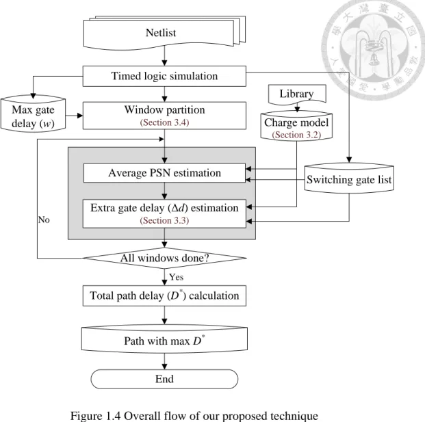
In this thesis, we propose a PSN-aware dynamic timing analyzer, IDEA (IR-Drop- aware Efficient timing Analyzer). Figure 1.4 shows the overall flow of IDEA. After performing timed logic simulation, the information of every switching gate is obtained.
In window partition, IDEA partitions a clock period into non-overlapping windows. In every window, charge model for a switching gate is obtained from Synopsys library (.lib) file and is used in average PSN estimation. IDEA performs extra gate delay estimation for every switching gate in this window. If there is no more windows to process, IDEA produces PSN-aware path delay by total path delay calculation, which is the summation of all nominal gate delay and extra gate delay on the path. Finally, IDEA reports path with maximum total path delay for every test pattern.
5 Timed logic simulation
Window partition (Section 3.4)
All windows done?
End Yes
Extra gate delay (Δd) estimation (Section 3.3)
Average PSN estimation
No
Path with max D* Max gate
delay (w)
Total path delay (D*) calculation Netlist
Charge model (Section 3.2)
Library
Switching gate list
Figure 1.4 Overall flow of our proposed technique
In our experiments, IDEA has been applied to two cases. One case only considers the impact of IR-drop on path delay and the other considers both Ldi/dt and IR-drop.
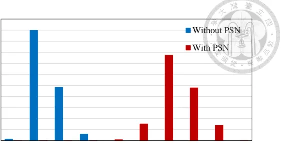
The results indicate the need for considering both Ldi/dt and IR-drop during dynamic timing analysis. Figure 1.5 shows path delay without PSN and with PSN (X axis) for the benchmark circuit leon3mp (1M gates). Y axis shows the number of test patterns in every interval. The histogram shows the importance of PSN since path delay increases significantly due to PSN.
6
Figure 1.5 Histogram of path delay without PSN and with PSN (leon3mp)
Our tool has three advantages over traditional techniques. 1) IDEA models gate delay as linear equations, instead of nonlinear equations, so the runtime is very short. 2) IDEA models gate delay as a function of charges, instead of voltage, so that gate delay can be modeled accurately without database characterization. 3) IDEA considers both Ldi/dt and IR-drop altogether. In spite of the above, our tool has a limitation: the number of continuous clock cycles is limited by accumulated PSN error. The reason is that we use window width (about ninety times larger than a time step) as a time unit of simulation.
1.3 Contributions
This thesis has the following contributions to the research of PSN-aware dynamic timing analyzer.
0K 2K 4K 6K 8K 10K 12K 14K 16K 18K 20K 22K
0.5~1.0 1.0~1.5 1.5~2.0 2.0~2.5 2.5~3.0 3.0~3.5 3.5~4.0 4.0~4.5 4.5~5.0 5.0~5.5
Number of patterns
Path delay (ns)
Without PSN With PSN
7
IDEA accurately estimates extra path delay, whose error is less than 1% compared
with a commercial circuit simulator, HSPICE.
IDEA achieves eight times speed up compared with a commercial tool, NANOSIM.
IDEA models extra gate delay as functions of charge, so there is no characterization
cost.
IDEA dynamically analyzes PSN-induced extra delay by solving both Ldi/dt and IR-
drop altogether.
1.4 Organization
The rest of the thesis is organized as follows. Chapter 2 reviews previous work about PSN estimation, extra gate delay calculation and PSN-aware timing analysis.
Chapter 3 describes the details of IDEA. Chapter 4 shows experimental results on benchmark circuits. Chapter 5 is the discussion. Chapter 6 concludes this thesis.
8
2
Chapter 2 Background
It has been shown that PSN cannot be ignored during timing analysis [Liou 2003].
PSN-aware timing analysis consists of two steps: PSN estimation and extra gate delay calculation [Wang 2006]. Section 2.1 summarizes past researches about PSN estimation.
Section 2.2 summarizes past researches about translation from PSN to extra gate delay.
Section 2.3 summarizes past researches about PSN-aware timing analysis.
2.1 PSN Estimation
PSN is the noise on the power grid and ground grid, which is modeled as an RC or RLC network. However, for VLSI system design, circuit simulation of such a complicated network is infeasible, due to long runtime and memory limitation [Nassif 2000][Pant 2003][Wang 2006]. We summarize two solutions to estimate PSN without intensive computation. One solution is PSN model; the other is fast power grid analysis.
We review three simple PSN models, which are often used in past researches. In [Wen 2005][Wen 2007], flip-flop toggle count (FFTC) is defined as
1 NF
i i
FFTC S
(2.1), where Si is the number of switches of flip-flop i and NF is the total number of flip-flops.
In [Ahmed 2007], switching cycle average power (SCAP), which is the average power consumed by a test pattern during the critical path delay (D), is defined a s
9
2
1 NG
j j
C VDD
SCAP D
(2.2), where Cj is the output capacitance of logic gate j, VDD is the nominal power supply voltage and NG is the total number of logic gates. In [Girard 2002][Remersaro 2006], weighted switching activity (WSA) is defined as
1 NG
j j j
WSA S F
(2.3), where Sj is the number of switches of logic gate j, Fj is the number of fan-out logic gates.
These three metrics have no consideration on resistance and capacitance of the power grid, location of switching gates and power pads. Hence, it has been shown that these metrics do not correlate well with PSN [Varma 2012][Ding 2013].
The above simple PSN models are computationally efficient but inaccurate.
Therefore, we introduce three power grid analyses for RC or RLC network with much shorter runtime than SPICE [Nassif 2000][Zhu 2003][Davis 2010].
In these three metrics, the analysis of RC or RLC network can be expressed as the
following differential equation, which uses MNA formulation:
G V C V I (2.4)
G is called conductance matrix. C includes the matrix of capacitance and inductance.
V is the solution vector composed of node voltages and inductor currents. V is the first derivative of V with respect to time. To obtain the solution, backward Euler method
10
(BE) is used to approximate V . Equations (2.5) to (2.7) show the derivation of applying BE method to equation (2.4). h is the time step size.
(th) ( )t h (th)
V V V (2.5)
( ) ( )
( ) t h t ( )
t h t h
h
V V
G V C I (2.6)
1
(t h) (t h) ( )t
h h
C C
V G I V (2.7)
In equation (2.7), if h holds constant, only one initial matrix inversion is required. For large circuits, since the matrix inversion typically dominates the runtime of power grid analysis, the use of a constant h results in large savings.
A power grid reduction has been proposed in [Nassif 2000]. In all power grid nodes, only nodes at extremities of rows/columns and at intersection of a row and a column are kept, kept nodes; other nodes are removed, removed nodes. The nodes in reduced power grid are first solved. The voltage of a removed node is calculated by a linear function, which includes voltages of neighboring kept nodes and conductance between the removed node and neighboring kept nodes. Since the size of reduced power grid is much smaller than original power grid, runtime and memory needed are significantly reduced.
Due to the timing of switching gates, PSN exhibits spatial variation, which means some power grid nodes have more rapid voltage variations than other power grid nodes.
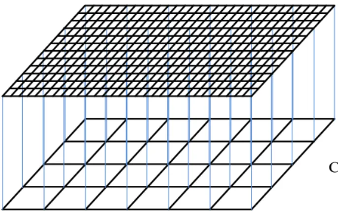
An adaptive algebraic multigrid method has been proposed in [Zhu 2003]. The basic
11
concept of multigrid is defining a hierarchy of a power grid, as shown in Figure 2.1.
Every node at coarse grid level represents a set of nodes at fine grid level. In adaptive algebraic multigrid method, active regions with more PSN have relatively finer grid at coarse grid level since active regions need more computation to model their behavior accurately. The technique is used to speed up power grid analysis, taking advantage of the spatial variation of PSN.
Fine grid level
Coarse grid level
Figure 2.1 Concept of multigrid
These two techniques mentioned above are too expensive for practical use in estimating PSN [Wang 2006]. KLU is a sparse LU factorization algorithm, which can deal with sparse asymmetric matrices [Davis 2010]. KLU performs three steps. (1) The matrix is permuted into Block Triangular Form (BTF), a symmetric permutation that makes the matrix block upper triangular. (2) The Approximate Minimum Degree (AMD)
ordering is used to fill-reducing order every block prior to LU factorization. (3) Gilbert/Peierls’ left-looking LU factorization algorithm with partial pivoting is used to
factorize every block. The total runtime is reduced since every block size is small.
12
2.2 Extra Gate Delay Calculation
PSN can induce extra gate delay and degrade circuit performance [Tehranipoor 2010]. We summarize four important techniques in recent research papers to calculate extra gate delay induced by PSN.
Extra gate delay is required to compute PSN, which is in turn required to compute extra gate delay. The first method proposed a procedure with iterative computation [Okumura 2010]. The procedure calculates average PSN during one time step at first, and then iteratively increases the number of time steps. Extra gate delay is calculated by a voltage-delay characteristic function, which is the function used to translate PSN to extra gate delay. After n iterations, if the difference between n×h and extra gate delay is smaller than h, the procedure finishes. h is the time step size. Since the time step is small, the method is accurate but slow.
For every gate in the library, SPICE simulation is performed under different conditions, such as transition type, power supply voltage of driver gate and receiver gate, input transition time, and output capacitance. The voltage-delay characteristic function can be stored in a database [Wang 2007][Aparicio 2013]. Translation from PSN to extra gate delay is done by table look-up, so runtime is short and the error is small. Since the database is obtained by intensive circuit simulation, the characterization cost is high.
The third method models the voltage-delay characteristic function as a regression
13
polynomial function [Wang 2006][Todri 2012]. For every gate in the library, SPICE simulation is performed under different conditions, which is the same as the second method, in order to compute extra gate delay variations. Then coefficients for regression polynomials are calculated. Since intensive circuit simulation is needed, the advantage and the disadvantage is the same as the second method.
In the second method, SPICE simulation is performed under a lot of different conditions to build the database, so the characterization cost is extremely high. To avoid such intensive circuit simulation, the third method proposed the voltage-delay characteristic function using equivalent output capacitor [Hashimoto 2004] or equivalent power supply voltage [Hashimoto 2008], which is compatible with static timing analysis.
Equivalent output capacitor and equivalent power supply voltage are used to reduce the number of parameters in the voltage-delay characteristic function. The goal of equivalent output capacitor is equalizing power supply voltages of driver gate and receiver gate, which causes charging/discharging current variation [Hashimoto 2004].
Equivalent output capacitor, which means increasing/decreasing the output capacitance in the same ratio as current variation, is used to keep the extra gate delay unchanged.
Average power supply voltage is used as equivalent power supply voltage [Hashimoto 2008].
TABLE 2.1 shows the comparison of techniques among recent research papers.
14
The third column ‘Circuit’ shows circuits used in experimental results. The fourth column ‘Error’ shows the error compared with SPICE. These techniques were applied
to small sample circuits only (such as NAND, INV and NOR).
TABLE 2.1 Comparison of previous translation from PSN to extra gate delay
2.3 PSN-Aware Timing Analysis
There are existing researches about PSN-aware timing analysis, which perform on circuits to ensure both good test quality and low yield loss. We summarize three important techniques in recent research papers for PSN-aware timing analysis.
Extra gate delay, which is obtained by the database, is used to update static standard delay format (.sdf) by considering PSN effect and generate pattern-dependent dynamic .sdf file for PSN-aware timing analysis [Peng 2010]. The database stores the
Ref. Method Circuit Error
[Hashimoto 2004] Equivalent Ten INV Average error is 1.6%
[Hashimoto 2008] Equivalent Ten INV Average error is 0.5%
[Okumura 2010] Iterative
INV, NAND and NOR.
Error ranges from -2%
to 2%
[Aparicio 2013] Database One INV Maximal error is 0.35%
[Todri 2012] Regression Three INV Error is 3.2%
15
voltage-delay characteristic function. Since the database is used to translate PSN to extra gate delay, characterization cost is high.
A gate-level event-driven simulator with two kinds of pre-characterized database is used for PSN-aware timing analysis [Jiang 2013]. PM is the first database, which is used to store PSN characteristic function, and TM is the second database, which is used to store the voltage-delay characteristic function. For every set of simultaneous events, PSN is calculated by PM and then extra gate delay is obtained by TM. The start time of the following events is updated by extra gate delay. There are two kinds of database that need to build, so characterization cost is much higher.
With performance and memory limitations of SPICE simulation, it is impossible for an entire VLSI system design. SPICE simulation is performed on critical paths, which is extracted by static timing analyzer, under transient PSN waveform [Apache 2011].
Both SPICE and transient PSN waveform simulation are accurate but slow when applied on big circuits. Besides, critical paths can change owing to extra gate delay induced by PSN, so the critical path delay obtained by this method may not be the worst case.
TABLE 2.2 shows the comparison of techniques among recent research papers.
The second column ‘Technique’ shows the main concept of PSN-aware timing analysis.
The third column ‘Method’ shows the main concept of translation from PSN to extra gate
delay used in the technique. The fourth column ‘Circuit’ shows circuits used for timing
16
analysis. The fifth column ‘Error’ shows PSN-aware path delay error compared with
SPICE. Technique ‘Dynamic .sdf file’ showed only correlation but not accuracy [Peng 2010]. Technique ‘Two kinds of database’ used a benchmark circuit of 30K gates [Jiang 2013]. Their runtime for p45 was 13 seconds per test pattern, which is still too slow for practical use. Therefore, there is still no general and efficient method to perform PSN- aware timing analysis so far.
TABLE 2.2 Comparison of previous PSN-aware timing analysis
Ref. Technique Method Circuit Error
[Peng 2010] Dynamic .sdf file Database s344 (32 gates)
Correlation coefficient is 0.95
[Jiang 2013]
Two kinds of database
Database p45 (30.6K) N.A.
IDEA [This work]
Window partition
Linear function
b17 (32.5K)
Average error is 25.5%
17
3
Chapter 3 Proposed Techniques
We propose a new timing analyzer, IDEA, based on observations in Chapter 2. The advantages of IDEA are as follows. (1) We use windows, which is much larger than a time step but smaller than a clock period, to find good balance between accuracy and runtime. We do not need to calculate transient PSN for every time step. Instead, we only need to calculate average PSN in a window. Silicon data have been shown that average PSN correlates well with extra gate delay [Saint-Laurent 2004][Ogasahara 2007].
(2) IDEA models gate delay as a function of charges so that we do not need the voltage- delay characteristic function. There is no need for SPICE simulation and characterization. (3) IDEA is a dynamic timing analyzer, so the timing of every test pattern is considered accurately. In spite of the above, our tool has a limitation. The number of continuous clock cycles is limited by accumulated PSN error. As the number of clock cycles increases, the error of Ldi/dt increases. For more details, please see the Discussion Chapter.
3.1 Overall Flow
Figure 3.1 shows the overall flow of IDEA for a single test pattern.
18 Timed logic simulation
Window partition (Section 3.4)
All windows done?
End Yes (1)
(2)
(7)
Extra gate delay (Δd) estimation (Section 3.3)
(4)
Average IR-drop estimation (3)
No
(5)
Path with max D* Max gate
delay (w)
Total path delay (D*) calculation (6)
Netlist
Charge model (Section 3.2)
Library
Switching gate list
Figure 3.1 IDEA flow (for a single test pattern)
1) Perform timed logic simulation on the test pattern to obtain the information of every switching gate. Charge model for every switching gate, which will be detailed in Section 3.2, is obtained from the Synopsys library (.lib) file.
2) Use maximum gate delay as window width, w, which is used to set the boundary for every window. Window partition will be detailed in Section 3.4.
3) Select the first un-simulated window and then perform average PSN estimation for this window.
19
4) Perform extra gate delay (Δd) estimation to calculate PSN-induced extra gate delay for every switching gate in this window. Extra gate delay estimation will be detailed in Section 3.3.
5) If there is no more windows to process, move on to step 6; otherwise, continue the next un-simulated window and then repeat steps 3 and 4.
6) Calculate total path delay (D*), which is obtained by
D* D D (3.1)
, where D is the path delay without PSN and ΔD is the PSN-induced extra path delay.
ΔD is calculated by summing up Δd for every path.
7) Report path with maximum D* for the test pattern. If D* is larger than the clock period, this circuit may fail this test pattern owing to excessive PSN.
3.2 Charge Model
We use charge model to describe the relationship between PSN and extra gate delay.
Charge model for every switching gate is used to calculate average current, average PSN and Δd for every window. The total energy consumed by a switching gate can be divided
into internal energy and switching energy [Synopsys 2008]. Therefore, we separate Q into internal charge (QIN) and switching charge (QSW). The internal energy, which is consumed by short circuit current, is equal to p×τI. p is the internal power and τI is the input transition time of the switching gate, which can be looked up in the Synopsys library
20
(.lib) file. We use equation (3.2) to calculate QIN, where VDD is the nominal power supply voltage. The switching energy is consumed by charging or discharging the capacitor. We use equation (3.3) to calculate maximum charge stored in the capacitor (QSW), where C is the capacitance.
I IN
Q p
VDD
(3.2)
QSW C VDD (3.3)
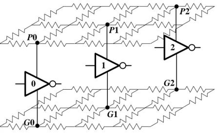
TABLE 3.1 shows average current in different conditions. Let P and G denote a power node and a ground node, respectively. Let R and F denote the output rising condition and the output falling condition, respectively. Every gate connects to P and G, as shown in Figure 3.2. P0, P1 and P2 are power nodes. G0, G1 and G2 are ground nodes.
P1
G1 P0
P2
G0 0 G2
1
2
Figure 3.2 Example of power nodes and ground nodes
I̅PR and I̅GR are average rising current flowing out of P and average rising current
21
flowing into G, respectively. I̅PF and I̅GF are average falling current flowing out of P and average falling current flowing into G, respectively. Figure 3.3 shows average current for output rising condition and output falling condition. In Figure 3.3(a), switching current for the output rising condition is flowing out of P to the capacitor, so QSW/w is only added to I̅PR, not to I̅GR. Similarly, in Figure 3.3(b), switching current for the output falling condition is flowing into G from the capacitor, so QSW/w is only added to I̅GF, not to I̅PF.
VDD
τI
GND
C Q
INw Q
SWw
VDD
GND
τI
C Q
INw
Q
SWw
(a) (b)
Figure 3.3 Average current for (a) output rising and (b) output falling TABLE 3.1 Average current cases
Output rising Output falling Power node
(current flows out of P)
IN SW
PR
Q Q
I w
PF IN
I Q
w
Ground node (current flows into G)
GR IN
I Q
w GF QIN QSW
I w
22
3.3 Extra Gate Delay (Δd) Estimation
Gate delay is the time between gate input transition and gate output transition, when they reach 50% VDD. Nominal gate delay (d) is the gate delay without PSN, which is
obtained from the standard delay format (.sdf) file. Δd is the PSN-induced extra gate delay. We need to estimate Δd for every switching gate so that we can calculate the gate
delay (d*) under PSN effect.
d* d d (3.4)
Figure 3.4 shows an inverter with rising output. We use gate 1 and gate 2 to represent a driver gate and a receiver gate, respectively. In this thesis, we use this figure as an illustration example to estimate gate delay. vI1 and vI2 are input voltage of gate 1 and gate 2, respectively. vO1 and vO2 are output voltage of gate 1 and gate 2, respectively.
They are functions of time, so they are denoted in small letters.
C
vO2
vI2
iD
VDD
GND
GND
(a)
GND VDD
VR2
VDD
GND
vI2
vO2
(b)
R2 δR2
(3.10)
(3.12) (3.7)
1
1 2F
2VDD
1 2 1
2VDD 1
Figure 3.4 Example of rising gate delay estimation of gate 2
23
To estimate ΔdR2, which is the rising extra gate delay of gate 2, we use
*
2 2
2 R R
dR d d
(3.5)
, where R2 is the estimated rising gate delay of inverter 2 without PSN and * R2 is the estimated rising gate delay of inverter 2 with PSN. In this thesis, the hat symbol means the value is estimated and the asterisk symbol means the value is PSN-aware.
Figure 3.4(b) shows how to estimate R2. Equation (3.6) is used in the estimation.
( )2
D 2 GS TH
i v V
(3.6) , where iD is the drain current through MOS, β is the transconductance coefficient of MOS, vGS is the voltage between transistor gate and source and VTH is the threshold voltage of MOS. Although we use level-1 quadratic model in this derivation, the conclusion of our work can be applied to other more accurate models. We will show that the conclusion is insensitive to the model in the Discussion Chapter. β and VTH can be accessed in the
MOS model, not in gate-level simulation. Therefore, two approximations are used to obtain ΔdR2, which will be detailed below.
iD represents the current flowing out of P. One part of iD is the short circuit current, which flows into G. The other part of iD is switching current, which flows into the capacitor. The former is about a hundred times smaller than the latter. Therefore, we assume that switching current is equal to iD.
In Figure 3.4, since vGS changes during input transition, R2 estimation is divided into
24
two parts. One is the delay before vI2 reaches its GND; the other is the delay after vI2
reaches GND. The former is equal to half of input transition time of gate 2, which is equal to half of output transition time of gate 1. τF1 is the falling output transition time of gate 1. The latter is defined as δR2.
2 1 2
1
R 2 F R
d (3.7)
τF1 can be looked up from the .lib file, so we only needto calculate δR2. We use equations
(3.8) to (3.10) to calculate VR2, which is the output voltage vO2, when vI2 reaches GND.
VR2 is a DC value, so it is denoted in capital letters.
2 O
D
Cdv i
dt (3.8)
2 1 2
2 0 2
1 ( )
2
R F
V
O I TH
C
GNDdv
S t V dt (3.9)3 2
2
( )
R 6 TH
I
V VDD V
C S
(3.10)
2
1 I
F
VDD GND
S
(3.11)
SI2 is the input slope of gate 2, which can be derived from τF1.
Equation (3.12) calculates δR2 which is based on C×ΔvO2/iD = ΔQ/iD. We can obtain the delay after vI2 reaches GND, as shown in equation (3.13), by substituting equation
(3.10) into equation (3.12). δR2 is measured as the delay from vO2=VR2 to vO2=0.5VDD.
2 2
O R
D
C v
i
2
2
1 2 1 2
R
TH
C VDD V
VDD V
(3.12)
25
2 2
2
1 2 1
1 3
2
R TH
TH I
C VDD
VDD V VDD V S
(3.13)
Second, we use similar way to calculate * R2, the estimated gate delay with PSN.
* *
2 1 1 2
1( )
R 2 F F R
d (3.14)
In equation (3.14), δ* R2 is the delay after vI2 reaches GND under PSN effect. S* I2 is the input slope of gate 2 with PSN effect.
* 2 2 1
2 *
2 2
2 1
(1 )
( )
2
1 3
( )
2
L H L TH
R
H L TH I
C VDD V
V V V
V V V S
(3.15)
* 1 1
2
1 1
H L
I
F F
V V
S
(3.16)
ΔτF1 is the PSN-induced extra falling output transition time of gate 1. The estimation of ΔτF1 will be detailed below.
In Figure 3.5, the waveform shows the output transition considering PSN. VH0 and VL0 are the power voltage of gate 0 and ground voltage of gate 0. VH1 and VL1 are the power voltage of gate 1 and ground voltage of gate 1. VH2 and VL2 are the power voltage of gate 2 and ground voltage of gate 2.
26
1 2
VH1
VL1
VH2
VL2
τF1+ΔτF1 VL0
VH0
0
Figure 3.5 Example of I/O waveform considering PSN
To obtain the values of power voltage and ground voltage for every gate, we solve
G V + C V = I matrix to calculate average PSN and average ground bounce. The I
vector is obtained from TABLE 3.1. Silicon data have been shown that average PSN correlates well with extra gate delay [Saint-Laurent 2004][Ogasahara 2007][Hashimoto 2008]. Values of VH0, VH1 and VH2 can be substituted by VDD minus average PSN of the window. Values of VL0, VL1 and VL2 can be substituted by average ground bounce of
the window.
Finally, we calculate ΔdR2 by substituting equation (3.7) and (3.14) into equation
(3.5).
2 2
2 2
2 1
1 1
( )
2 2
1 1
( ) ( )
2 2
L R
H L TH TH
C VDD V C VDD
d
V V V VDD V
(3.17)
2 *1 1
2 2
( ) ( )
3 3 2
TH H L TH F
I I
VDD V V V V
S S
VTH cannot be accessed in gate-level simulation, so we need to remove it from equation (3.17). Since SI2 and S* I2 are very large, we can make this approximation:
27
*
2 2
3 3 0
TH TH
I I
V V
S S (3.18)
2
2 1 1
2 *
2 2 2 2
2 1
1 1
( )
( )
2 2
1 ( ) 1 ( ) 3 3 2
2 2
L
H L F
R
I I
H L TH TH
C VDD V C VDD
V V d VDD
S S
V V V VDD V
(3.19)
Output transition time is the time between GND and VDD of gate output transition.
Nominal output transition time (τ) is the output transition time without PSN, which can be obtained from the .lib file. Δτ is the PSN-induced extra output transition time, which is needed for estimating output transition time (τ*) under PSN effect.
We use a model to calculate output transition time, which is proposed in [Maurine 2001]. In equation (3.20), τ F1 and τ * F1 are the estimated falling output transition time of
inverter 1 without PSN and with PSN, respectively.
*
1 1
1= F F
τF τ τ
1 1
2 2
0 1
( ) ( )
1 1
( ) ( )
2 2
H L
H L TH TH
C V V C VDD GND
V V V VDD V
(3.20)
In equation (3.19) and (3.20), the values of β and VTH are not determined yet. Thus we use peak current to replace the current in these equations, like equations (3.21) and (3.22).
2
1 2 1
2 * *
2 2 2
2
1 1
( )
2 2
2 3 3
L
F H L
R
PR I I
PR
C VDD V C VDD
V V d VDD
S S
I I
(3.21)
28
1 1
1 *
1 1
H L
F
GF GF
V V VDD GND
τ C
I I
(3.22)
ĨPR2 and Ĩ * PR2 are peak current for output rising of gate 2 without PSN and with PSN,
respectively. ĨGF1 and Ĩ * GF1 are peak current for output falling of gate 1 without PSN and with PSN, respectively.
To calculate the value of peak current, we use the equalization of charge to explain the derivation. Equation (3.23) shows the integral of iD and we assume dR2≫0.5τF1. One part of iD is the short circuit current. Since the duration of dR2 only include half of input transition time, the charge is equal to 0.5×QIN. The other part of iD flows through the capacitor for charging. Since the range of vO2 variation during dR2 is 0.5×VDD, the charge is equal to 0.5×QSW. Therefore, QD is equal to 0.5×(QIN+QSW). I̅PR2 is I̅PR of gate 2.
2 2
0 2
dR
D GS TH
Q
v V dt(3.23)
1 2
1
1
2 2
2 1
0 2 2 2
F R
F
d
GS TH TH
v V dt VDD V dt
22 2
R TH D
d VDD V Q
2
1
2 2
SW IN
D D
PR
Q Q
Q Q
w w w I
(3.24)
We substitute equation (3.23) into equation (3.24) and obtain
22 1 2
2 2
R TH PR
d VDD V I
w
(3.25)
29
Therefore, ĨPR2 in equation (3.21) is obtained.
2 2
2 2
PR PR
R
I I w
d (3.26)
Figure 3.6 shows the current waveform of I̅PR2 and ĨPR2. The area of these two rectangles presents charges. QSW and QIN can be calculated from the .lib file. Since QD is equal to 0.5×(QIN+QSW), the two rectangles are the same in area. They are different by the width.
One is window width w, the other is gate delay dR2.
t i
d
R2w
2
I
PR1 2
2
I
PRQ
D
1
2
Q
SW Q
INFigure 3.6 Current waveform transformation
Similarly, Ĩ * PR2, ĨGF1 and Ĩ * GF1 in equations (3.21) and (3.22) are calculated by:
* 1 2 2
2
1 1 2 2
2 2
H L
PR F
H L R R
C V V I p
V V d d
(3.27)
1 0
1 1
2 2
GF R
F F
p C VDD
I VDD d d
(3.28)
* 0 1 1
1
0 0 1 1
2 2
H L
GF R
H L F F
C V V I p
V V d d
(3.29)
We substitute equations (3.37) to (3.39) into equations (3.21) and (3.22) and obtain equations (3.30) and (3.31).
30
2
1 2 1
2 *
2 2 1 2 2
1
2 2
1 1 2 2
1 1
( )
2 2
2 3 3
2 2
2 2
L
F H L
R
H L F I I
F
R R
H L R R
C VDD V C VDD
V V d VDD
p C VDD
C V V S S
p
VDD d d
V V d d
(3.30)
1 1
1
1 1 0
0
1 1
0 0 1 1 2 2
2 2
H L
F
H L R R
F F
H L F F
V V VDD GND
τ C
p C VDD
C V V
p
VDD d d
V V d d
(3.31)
In these two equations, we model extra gate delay and extra output transition time as function of charges, but not current model. Therefore, the impact of applying
different drain current model is small.
We use similar way to estimate ΔdF2 and ΔτR1, as shown in equations (3.32) and
(3.33).
2
1 1 2
2 * *
2 2 2
2
1 1
( )
2 2
2 3 3
H
R H L
F
GF I I
GF
C V VDD C VDD
V V d VDD
S S
I I
(3.32)
1 1
1 *
1 1
H L
R
PR PR
V V VDD GND
C I I
(3.33)
,where ĨGF2 and Ĩ * GF2 are peak current for output falling of gate 2 without PSN and with PSN, respectively. ĨPR1 and Ĩ * PR1 are peak current for output rising of gate 1 without PSN and with PSN, respectively.
2 1
2 2
2 2
GF R
F F
p C VDD
I VDD d d
(3.34)
* 1 2 2
2
1 1 2 2
2 2
H L
GF R
H L F F
C V V I p
V V d d
(3.35)
31
1 0
1 1
2 2
PR F
R R
p C VDD
I VDD d d
(3.36)
* 0 1 1
1
0 0 1 1
2 2
H L
PR F
H L R R
C V V I p
V V d d
(3.37)
3.4 Window Partition
Since a single clock period is long, average PSN estimation for a whole clock period is not accurate enough. According to [Devanathan 2007][Wen 2008][Wu 2010], the window partition improves the average PSN estimation quality because the temporal requirement of switching gates is taken into consideration. Therefore, we divide a whole clock period into several non-overlapping equal-length time slices, called windows.
We need to decide the window width, w. If w is too large, average PSN is very low so Δd can be underestimated. On the contrary, if w is too small, we see a scenario where
d of a switching gate crosses window boundaries. Figure 3.7 illustrates such a scenario.
d1 is the partial gate delay in window 1 and d2 is the partial gate delay in window 2. For such a scenario, it is not clear that the charge of this switching gate contributes to which window.
d1 d2
Window 1 Window 2
d
Figure 3.7 Switching gate delay crosses a window boundary
![Figure 1.1 Comparison of extra delay ratio between 180nm and 45nm [Okumura 2010]](https://thumb-ap.123doks.com/thumbv2/9libinfo/9606763.632707/11.892.286.606.850.1097/figure-comparison-extra-delay-ratio-nm-nm-okumura.webp)
![Figure 1.2 IR-drop maps (a) without package effects and (b) with package effects [Cadence 2009]](https://thumb-ap.123doks.com/thumbv2/9libinfo/9606763.632707/12.892.136.762.724.1013/figure-drop-maps-package-effects-package-effects-cadence.webp)