Design and Implementation of Boost-type Flyback PV Inverter
S. J. Chiang, T. T. Ma, and M. J. Lee
Department of Electrical Engineering, National United University, Miao-Li 360, Taiwan, ROC [email protected]
Abstract- This paper presents a PV inverter system formed by a DC-DC converter and a full-bridge DC-AC converter.
The DC-DC converter combines the boost and flyback topologies to produce a semi-sinusoidal output current and to achieve the high step-up objective. A full-bridge DC-AC converter controlled with low-frequency switching techniques is then used to convert the current into sinusoidal form and to feed power to the grid with unit power factor.
The overall efficiency of the designed system is high due to the losses of both stages are reduced. The circuit operating theory of the proposed PV inverter is firstly addressed then an 80W prototype system is designed and built. The feasibility and effectiveness of the proposed circuit are confirmed with some simulation and experimental results.
Index Terms-boost converter, flyback converter, grid connected PV inverter
I. INTRODUCTION
With the ever growing concern about global warming, environmental pollution, and the rising cost of fossil fuels like oil and coal, there is a greater interest in developing distributed generations (DG) with renewable energy sources (RES) to meet the growing energy demand. Of these renewable energy sources, photovoltaic (PV) technologies are becoming cost-effective today in an increasing number of markets, and are making important steps to broader commercialization.
In addition to central PV inverter systems which are normally designed with relatively high power ratings, the application of small dispersed PV complementary energy systems is another rapidly growing area [1, 2] and is developed toward architectures consisting of a number of PV inverters with relatively small power ratings and which can be incorporated into roofing materials or dispersedly installed at any location in the building near an outlet. The number of PV module in the applications of this kind is around 1---5 per inverter, and there will be as many inverters as the application needs. However, the key to the success of applying small dispersed PV energy systems is a simple, low cost and high performance inverter.
This paper starts with an overview of some existing staged power inverter topologies for interfacing PV modules to the grid. Other reported approaches are further discussed and evaluated in order to recognize the advantages of the proposed PV inverter system. Next, followed the design concept and the circuit operating theory of the proposed PV inverter an 80W prototype system is designed and built. The feasibility and effectiveness of the proposed circuit are confirmed with some simulation and experimental results.
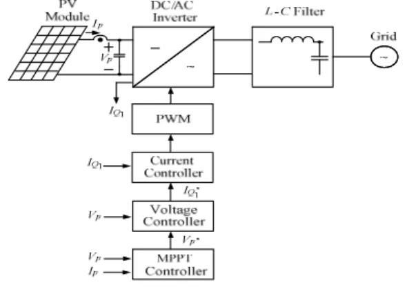
II. PV INVERTER TOPOLOGY OVERVIEW The PV inverter topologies can be categorized on the basis of number of power processing stages [3]. Fig. 1 is a single-stage inverter which handles all tasks by itself, i.e., MPPT controller to generate optimal operating voltage
commands Vp*, grid current controller to obtain a low distorted sinusoidal waveform and to achieve the objective of feeding high power factor power to the grid. Simple circuit and controller design are its advantages; however, a huge number of PV modules connected in series will be required to come up with an adequate voltage level for the dc linked interface. Fig. 2 depicts a dual-stage inverter.
The dc---dc converter is now working between the PV module and the dc linked capacitor and performing the MPPT and voltage amplification functions. The voltage source inverter is then used to control the power injected into the grid by means of high frequency pulse width modulation (PWM) technologies. The main drawbacks of this topology is overall efficiency being relatively low due to the two-stage energy conversion and the performance of the voltage sourced DC-AC converter being sensitive to the dynamics of the dc linked interface, the grid voltage variations and the transients of load switching. To improve some of the above mentioned disadvantages, this paper proposes an integrated version of two-stage PV inverter topology as shown in Fig. 3. In this design, a high efficiency DC-DC converter with current source output cascaded with a line-frequency switched DC-AC converter is utilized to achieve a high performance and cost effective PV inverter system.
Fig. 1. Single-stage inverter topology
Fig. 2 Dual-stage inverter topology
Fig. 3 An integrated version of dual-stage PV inverter scheme
III. OPERATING PRINCIPLES OF THE PROPOSED PV INVERTER
A. Circuitry and control arrangements
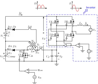
Fig. 4 shows the detail of the proposed inverter. A boost type flyback converter is employed to boost the voltage and generate the semi sinusoidal current waveform. A full-bridge inverter with line switching frequency is utilized to reduce the switching loss and unfold the output current of the DC-DC converter into a full sinusoidal waveform. The boost plus flyback converter is designed to increase output voltage gain with a flyback coupled inductor and recycle the leakage inductance energy with the boost output capacitor.
Fig. 4 The proposed boost type flyback PV inverter system
A low pass filter is constituted by a clamping capacitor Cclamp, connecting in series with C and the output inductor Ls. By cascading the output voltage VCc of the boost converter and the output voltage Vc of the flyback converter, a high output voltage, Vd, is easily obtained [4-7]. In addition, there is a low voltage stress imposed on the power switch and diode as well as on the output capacitors compared to that of conventional boost converters. The low side capacitor Cclamp functions as an output capacitor and a snubber capacitor to suppress the voltage spike on Q1, during the turn-off transient period, which also recycles the leakage energy in the coupled inductor. In this design, a power switch Q1, with low
voltage rating is used to reduce conduction loss, and as a result the overall efficiency is significantly improved.
For the switching control of the proposed PV inverter system, a semi sinusoidal pulse width modulation (PWM) method is utilized. The duty cycle of the switching device Q1 is obtained from comparing a sawtooth voltage waveform, Vtri, and a half-cycle sinusoidal voltage waveform. By setting the peak value of the current flowing through Q1 to be proportional to the grid voltage and controlling the converter under discontinue current mode (DCM), a half-cycle sinusoidal current waveform can be produced for the output current of the flyback converter, Id , which is also proportional to its primary current, i.e., the peak current of Q1, IQ1. In order to convert the half-cycle sinusoidal current waveform into an alternative current waveform, the switching signal for the full-bridge DC-AC converter is made synchronous to the grid voltage ,Vs. The switching devices, (TA+、TB-), of the inverter are turned on during the positive half cycle and the other pair of switches, (TA+、TB-), are turned on during the followed negative half cycle. The output of the full-bridge DC-AC converter is then connected to the grid (Vs) via a low pass filter formed by VCc and Cc and Ls to achieve feeding unit power factor power to the grid. It should be noted that overall efficiency can be further increased due to the discharging path of the clamping capacitor Cclamp does not include the diode.
B. Operating principles
To analyze the circuit of the proposed PV inverter shown in Fig. 4, the transformer T1 is modeled as a magnetizing inductance Lm and two leakage inductances Lk1 and Lk2, and an ideal transformer which consists of a turns ratio of Np/Ns. The typical current waveforms of the converter operated in DCM are illustrated in Fig. 5.
Figs. 6-13 illustrates all possible equivalent circuits operating within one switching cycle of the converter.
According to Figs. 6-13 the seven operational modes are described as follows:
Fig. 5 Typical current waveforms of the converter operated in DCM Mode I [t0–t1]: The equivalent circuit of this mode is shown in Fig. 6. When the switch Q1 starts to turn on at t0, The input voltage Vp is directly connected to the inductor and the current of the magnetizing inductance ILm is linearly increased. The peak value ILm,pk, is reached at the time instance t1 on which the switch Q1 is cut off and ILm,pk
can be expressed as follows:
, 1
p
Lm pk s
k m
I V DT
L L
= ⋅
+ (1) During this time interval, diodes D1 and D2 are reverse-biased. The output capacitors Cclamp and C supply energy to the grid via the output current of the flyback converter, Id and the switching devices, (TA+、TB-), of the inverter are turned on. The current injecting into the grid is positive within a positive half-cycle of the grid voltage.
Mode II [t1–t2]: The equivalent circuit of this mode is shown in Fig. 7. At the time instance, t1, the main switch, Q1 is cut off and the current of the magnetizing inductance ILm starts to charge the stray capacitor Cds. Before the voltage on Cds reaches the voltage of VCc, the output capacitors Cclamp and C continue to supply energy to the grid.
Mode III [t2–t3]: The equivalent circuit of this mode is shown in Fig. 8. At the time instance t2, the two diodes D1
and D2 are turned on due to forward biased. The voltage on the magnetizing inductance VLm is given by:
Lm Cc p
V =V −V (2) The voltage on the filtering capacitor Vc can be expressed as follows:
( )
c s Cc p
p
V N V V
= N ⋅ − (3) The currents flowing through the two diodes, ID1andID2, are
1 2 1'
Cc p s
D on D D
p
V V N
I t I I
Lm N
= − − ⋅ − ⋅ +
(4)
2 2'
2
( )
s
Cc p
p
D on D
k
N V V
I N t I
L
−
= ⋅ + (5)
In the above equations, ton=t3 - t2, and
2 1'
1 2
k
D Lm
k k
I L I
L L
= ⋅
+ (6)
2 ' 1
1 2
k p
D Lm
k k s
L N
I I
L L N
= ⋅
+ (7) The current ID1 is charging the clamping capacitor, Cclamp, to store energy from the leakage inductance. When the current of ICc is increased, the current of ID2 can not fully
support the output current, Id . The flyback capacitor C continues to contributes its energy to the grid via its discharging current.
Fig. 6. The equivalent circuit of Mode I [t0–t1]
Fig. 7. The equivalent circuit of Mode II [t1–t2]
Fig. 8. The equivalent circuit of Mode III [t2–t3]
Mode IV [t3–t4]: The equivalent circuit of this mode is shown in Fig. 9. At the time instance t3, the current of ID1
starts to decrease from its peak value and the current of ICc
is decreasing at the same time. In this time interval, the current ID1, is charging the clamping capacitor Cclamp, and providing current to the grid. The current of ID2 is linearly increased due to the discharging of the flyback capacitor C.
Mode V [t4–t5]: The equivalent circuit of this mode is
shown in Fig. 10. During this time interval, the current of ID2 is charging the flyback capacitor C and providing the output current Id. The current ICc flowing into the output capacitor becomes negative and transfers its energy to the flyback capacitor C to support the output current Id.
Mode VI [t5–t6]: The equivalent circuit of this mode is shown in Fig. 11. At the time instance t5 the current ID1
reaches zero and the current of ID2 is linearly decreased due to the voltage on the secondary winding is reversed.
This leads to the current of Ic stars to decrease and the current of ID2 reaches zero at the time instance of t6.
Mode VII [t6–t7]: The equivalent circuit of this mode is shown in Fig. 12. During this time interval, the two diodes D1 and D2, are reverse biased. The output current Id is provided by ICc and Ic.
Fig. 9. The equivalent circuit of Mode IV [t3–t4]
Fig. 10. The equivalent circuit of Mode V [t4–t5]
IV. DESIGN OF DEVICES
Referred to the equivalent circuit of Mode III as shown in Fig. 8, at the time instance t2 when the two diodes D1
and D2 are turned on due to forward biased the voltage imposed on the main switch, VDSS, equals to the voltage on the output capacitor. As depicted in Fig. 11, when the diode D1 is off and D2 is on the voltage imposed on the main switch VDSS is given by:
Fig. 11. The equivalent circuit of Mode VI [t5–t6]
Fig. 12. The equivalent circuit of Mode VII [t6–t7]
p
DSS p c
s
V V V N N
⎛ ⎞
= + ⋅⎜ ⎟
⎝ ⎠
(8)
From (3) and (8), VDSS =VCc. When the converter is operated in Mode VII, the two diodes D1 and D2 are off and the voltage imposed on the main switch VDSS equals to Vp. The value of VCc can be calculated by using Eq.(3) as:
( )
s
Cc c Cc Cc p d
p
V V V N V V V
+ = +N ⋅ − = (9) In Eq. (9), the voltage Vd is equivalent to the peak valued of the grid voltage. Rearranging Eq. (9), The voltage on the output capacitor can be mathematically expressed as follows:
p d s p
Cc
p s
N V N V
V N N
⋅ + ⋅
= +
(10)
V. SIMULATION AND EXPERIMENTAL RESULTS In this paper an experimental 80W PV system is constructed for test purposes. The details of the
experimental system are below:
Input voltage : 10-40 VDC
Grid voltage/frequency: 110V/60Hz Switching frequency: 20kHz PV module: 80W (VMPPT=15V)
Fig. 13 shows the details of the proposed 80W PV inverter system. The outer control loop is a maximum power point tracking (MPPT) controller which is in charge of calculating the operating voltage command Vp* for achieving the maximum power operation of the PV module. The inner loop is a voltage regulation loop designed for regulating the voltage of PV module Vp to approach the voltage command Vp*. To construct the control voltage vcon for the converter the output of the voltage controller is multiplied by a half cycle sinusoidal signal. The trigging signal for the main switching device of the flyback converter is obtained with the PWM.
sin tω
Fig. 13. The overall hardware configuration and controllers of the proposed PV inverter
A. Simulation results
Prior to hardware implementation the proposed PV inverter system is simulated in the PSIM software environment to confirm the performance of the designed controllers. Fig. 14 shows the simulation results. The proposed MPPT controller is able to find the voltage of 15V for the used PV module on the setting of maximum power point (VMPPT = 15V) and the voltage controller is also able to properly regulate the voltage of the PV module at 15V. Fig. 14 also shows that the simulated current injected into the grid is low distorted and almost in phase with the grid voltage. This ensures that a very high power factor can be obtained.
B. Experimental results
Based on the design concepts presented in the previous sections, an 80W grid connected PV inverter system is constructed and implemented with the DSP-based (dsPIC30F4011) controller. The measured results shown in Fig. 15 verify the simulation results presented above.
Fig. 14. The simulation results of the proposed PV inverter
Fig. 15. The measured results of the proposed PV inverter
References
[1] F. Giraud and Z. M. Salameh, “Steady-State Performance of a Grid-Connected Rooftop Hybrid Wind-Photovoltaic Power System with Battery Storage,” IEEE Transactions on Energy Conversion, Vol. 16, pp. 1-7, 2001.
[2] N. Kasa and T. Iida, “Flyback type Inverter for Small Scale Photovoltaic Power System,” IEEE IECON'02, Vol. 2, pp.
1089-1094, 2002.
[3] S. B. Kjaer, J. K. Pedersen and F. Blaabjerg, “A review of single-phase grid-connected inverters for photovoltaic modules,”
IEEE Transactions on Industry Applications, Vol. 41, No. 5, pp.
1292-1306, 2005.
[4] Copple, E. J. and Heights, A, “High Efficiency DC Step-up Voltage Converter ,” US Patent’, 1999.
[5] Q. Zhao, “Performance Improvement of Power Conversion by Utilizing Coupled Inductors,” Virginia Polytechnic Institute and State University of Doctor of Philosophy in Electrical Engineering, February 03, 2003.
[6] Q. Zhao and F. C. Lee, “High-efficiency, High Step-up DC-DC Converters,” IEEE Transactions on Power Electronics, Vol. 18, pp. 65-73, 2003.
[7] N. Kasa, T. Iida and Liang Chen, “Flyback Inverter Controlled by Sensorless Current MPPT for Photovoltaic Power System,” IEEE Transactions on Industrial Electronics, Vol. 52, pp. 1145-1152, 2005.
![Fig. 5 Typical current waveforms of the converter operated in DCM Mode I [t0–t1]: The equivalent circuit of this mode is shown in Fig](https://thumb-ap.123doks.com/thumbv2/9libinfo/9124095.408607/3.892.462.800.175.380/typical-current-waveforms-converter-operated-mode-equivalent-circuit.webp)
![Fig. 9. The equivalent circuit of Mode IV [t3–t4]](https://thumb-ap.123doks.com/thumbv2/9libinfo/9124095.408607/4.892.464.806.109.339/fig-equivalent-circuit-mode-iv-t-t.webp)

