sensors
ISSN 1424-8220 © 2007 by MDPI www.mdpi.org/sensors Full Research Paper
Fabrication and Characterization of PZT Thick Films for
Sensing and Actuation
Ling-Sheng Jang 12* and Kuo-Ching Kuo 2
1
Department of Electrical Engineering and Center for Micro/Nano Science and Technology, National Cheng Kung University, Tainan 710, Taiwan
2
Institute of Nanotechnology and Microsystem Engineering, National Cheng Kung University, Tainan 710, Taiwan; E-mail: [email protected]
* Author to whom correspondence should be addressed; E-mail: [email protected] Received: 16 February 2007 / Accepted: 4 April 2007 / Published: 18 April 2007
Abstract: Lead Zirconate Titanate oxide (PZT) thick films with thicknesses of up to 10 µm were developed using a modified sol-gel technique. Usually, the film thickness is less than 1 µm by conventional sol-gel processing, while the electrical charge accumulation which reveals the direct effect of piezoelectricity is proportional to the film thickness and therefore restricted. Two approaches were adopted to conventional sol-gel processing – precursor concentration modulation and rapid thermal annealing. A 10 µm thick film was successfully fabricated by coating 16 times via this technique. The thickness of each coating layer was about 0.6 µm and the morphology of the film was dense with a crack-free area as large as 16 mm2. In addition, the structure, surface morphology and physical properties were characterized by X-ray diffraction (XRD), scanning electron microscopy (SEM) and atomic force microscopy (AFM) and electrical performance. The dielectric constant and hysteresis loops were measured as electric characteristics. This study investigates the actuation and sensing performance of the vibrating structures with the piezoelectric thick film. The actuation tests demonstrated that a 4 mm x 4 mm x 6.5 µm PZT film drove a 40 mm x 7 mm x 0.5 mm silicon beam as an actuator. Additionally, it generated an electrical signal of 60 mVpp as a sensor, while vibration was input by a shaker. The frequencies of the first two
modes of the beam were compared with the theoretical values obtained by Euler-Bernoulli beam theory. The linearity of the actuation and sensing tests were also examined.
1. Introduction
Piezoelectric materials are extensively adopted owing to their many desirable characteristics. First, they can transform electrical signals into mechanical deformation. Hence, they can serve as actuators. They can also transform mechanical deformation into electrical signals, and so can serve as sensors. Additionally, some piezoelectric materials can be miniaturized to produce films or nano-wires for further applications. These films are important components of both actuators and sensors in MEMS and micro-optical devices such as micropumps, atomic force microscopes (AFM), ultrasonic micromotors [1], infrared (IR) detector arrays [2], micromixers [3], micromirrors, microrelaies [4], pressure microsensors [5, 6] and stress microsensors [7]. The applications of piezoelectric films are myriad. Recently, piezoelectric materials with high remnant polarization have attracted much interest as they have great potential in the preparation of memory devices [8]. High-quality actuation and sensing materials are required for well-performing MEMS devices.
PZT can generate a ten times larger force and 100 times larger acoustic power density than non-ferroelectric materials such as ZnO (zinc oxide) [9], SiO2 (quartz) and AlN (aluminum nitride) [10].
Three popular methods exist for fabricating PZT films - thick-film printing [11-13], sputtering [14, 15] and sol-gel processing [16-19]. The process of thick-film printing can easily form thick PZT films with thicknesses of between 10 and 100 µm. Sintering temperatures of over 850oC are required to yield adequate PZT particles. Sputtering is another familiar approach for synthesizing PZT films, which are typically less than 1 micron thick. Post-deposition annealing of sputtered films is required to crystallize the ferroelectric structure of the material. Sol-gel processing is a wet chemical method for synthesizing and processing inorganic hybrid materials. This work is based on sol-gel processing because it has three advantages. Firstly, it allows the convenient control of the stoichiometric chemical composition of lead zirconate titanate. Secondly, sol-gel processing is inexpensive, because it uses 100% of the precursors without expensive equipment. Finally, it can be used for mass production.
The sol-gel process is one of the most versatile and extensively employed techniques. Nevertheless, the piezoelectric characteristics of sol-gel-derived PZT films tend to be inferior to those of bulk PZT, mainly because of the small grain size of the derived PZT films, which, in turn, results from the homogeneous nucleation of many crystalline PZT nuclei during crystallization. The piezoelectric effects of the crystalline particles drop as the grain size declines. Therefore, homogeneous nucleation must be prevented to ensure favorable ferroelectric properties. The second reason for the inferior film properties is the limited film thickness. The thickness of a film formed by conventional sol-gel processing typically does not reach 1 micron, while the charge accumulation associated with the material electric dipole is proportional to the film thickness. Restated, the finite thickness of the film restricts actuation strength and sensing performance.
Two techniques were applied to increase the thickness of PZT films and reduce the duration of the fabrication process - precursor concentration modulation [20-21] and rapid thermal treatment [22]. The precursor concentration was modulated by applying particles to the PZT sol. Modulating the concentration of the sol increased the thickness of the film at each coating process. Homogeneous nucleation was thus prevented, and the sizes of the PZT grains increased. Rapid thermal treatment reduced the duration of heating and cooling, and thus reduced the overall duration of the fabrication process, increasing the convenience of batch processing for various applications. In this work, a
modified sol-gel approach based on rapid thermal annealing and a high concentration of PZT sol is utilized to yield a film of thickness 10 µm with a crack-free area as large as 16 mm2
. The films were characterized. Furthermore, the sensing and actuation capacities of the films were successfully demonstrated.
2. Fabrication
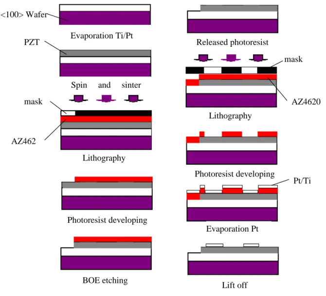
A 500 nm-thick silicon dioxide layer was first wet-thermally grown on a <100> silicon wafer that was 500 µm thick. Then, a 200 nm-thick layer of silicon nitride was deposited on the top of the silicon dioxide film by LPCVD (low-pressure chemical vapor deposition). An E-beam evaporator was then employed to grow the bottom electrode, with a 50 nm-thick layer of titanium and a 100 nm-thick layer of platinum. The PZT sol was next spun on a Pt(111)/Ti/SiN4/SiO2/Si substrate and patterned by
conventional photolithography, with BOE (buffered oxide etchant, HF (49%): NH4F (10%) = 6:1) and
an AZ4620 mask [19]. A 50 nm-thick layer of titanium and a 100 nm-thick layer of platinum was deposited and patterned on the PZT film as the top electrode. A lift-off process was applied to the top electrode to expose the PZT films and the bottom electrode for future measurements of electrical and mechanical characteristics. Figure 1 schematically summarizes the overall preparation procedure. Finally, a poling process was performed by applying 28 V/µm to the PZT films at 100 o
C for one hour. PZT sol was prepared using three precursors, Pb(CH3COO)2, Zr(C3H7O)4 and Ti((CH3)2CHO)4.
0.01 wt% PZT powder was added to increase the viscosity and concentration of the PZT sol. The sol was passed through a 0.22 µm in-line syringe filter directly before the film was prepared. The supplementary particles acted as seeds during the PZT annealing process and homogeneous nucleation was prevented to promote the growth of the PZT grains of the films. The sol was subsequently spin-coated on the substrate at 1500 rpm for 32 s. Each wet layer was initially dried at room temperature for 15 minutes to evaporate the solvent. It was then rapidly heated to 650 ℃ for 15 minutes to remove organics. The layer was crystallized in this step. Finally, PZT films of the desired thickness were formed by repeating the coating and heating procedures. Appendix A presents a detailed recipe of PZT sol.
Figure 1. Preparation of substrate.
3. Characterization of PZT Thick Films 3.1 Physical Characterization
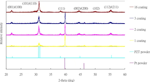
An XRD (X-ray diffraction, Rigaku D/MAX2500, Cu 40 kV 100 mA) study was performed on the PZT films with one, two, three and 16 coating layers, to prove that the sintered film had the correct chemical composition and was crystallized. Based on the profile of the XRD spectra presented in Fig. 2, the phase intensity of platinum was high when the number of PZT coating layers was under three. However, the effect of platinum on the phase becomes weaker as the number of PZT coating layers increases, probably because the effect of platinum is harder to be detected in thicker films. Therefore, the platinum phase is absent when the film has up to 16 coats. Additionally, the X-ray diffraction pattern reveals that the fabricated PZT film is perovskite phase with no pyrochlore phase. The XRD graph shows that the texture of the film exhibited a (110) orientation preference. The preparation of the sol solution, the spin-coating process and the heat treatment are effective for the phase development of PZT films.
Evaporation Ti/Pt
Spin and sinter
Lithography PZT Pt/Ti Photoresist developing mask AZ462 Released photoresist BOE etching Lithography Photoresist developing Evaporation Pt Lift off mask AZ4620 <100> Wafer
20 25 30 35 40 45 50 55 60 2-theta (deg) R el at iv e in te ns it y 16 coating 3 coating 2 coating 1 coating PZT powder Pt powder (001)/(100) (101)/(110) (111) (002)/(200) (102) (112)/(211)
Figure 2. XRD spectra of PZT powder, Pt and PZT films with one, two, three and 16 coating layers. 3.2 Observation of Morphology
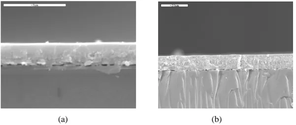
Figures 3 and 4 present the surface and cross-sectional images of 2 µm and 10 µm-thick films fabricated by modified sol-gel processing with precursor concentration modulation and rapid thermal annealing. The 2 µm and 10 µm-thick films were fabricated with three and 16 coating layers. These micrographs were obtained using FE-SEM (Field Emission Scanning Electron Microscope, PHILIPS, XL-40FEG) and MSEM (Multipurpose Scanning Electron Microscopy, JEOL JXA-840). According to the SEM images, the structure of the films is dense and crack-free. The thickness of each coating is about 0.6 µm, which is much thicker than the PZT films fabricated by conventional sol-gel processing [23]. Therefore, the supplementary PZT powders did not exhibit homogeneous nucleation; the growth of the PZT grains in the films was promoted and the film thickness increased. The surface roughness of the films was measured by AFM (Atomic Force Microscope, Veeco, CP П). Over a surface area of 5 µm x 5 µm, the average roughness was 2.2 nm.
(a) (b)
(a) (b)
Figure 4. Cross-sectional SEM image: (a) 2 µm-thick PZT film (scale bar represents 5 µm); (b) 10
µm-thick PZT film (scale bar represents 20µm). 3.3 Electrical Characterizations
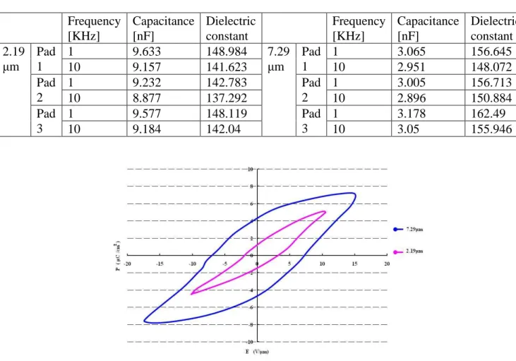
Table 1 presents the electric characteristics of the films which were evaluated by determining dielectric constants. The dielectric constants were measured at 1 and 10 kHz for two kinds of thickness: 2.19 and 7.29 µm. The measuring area of three different electrode pads (pad #1, 2 and 3 in Table 1) was 4 mm x 4 mm. The dielectric constants were from 142 to 148 for a thickness of 2.19 µm and from 156 to 162 for a thickness of 7.29 µm, respectively. The table reveals that thicker films had higher dielectric constants, and that the dielectric constants decreased as the frequency increased.
Figure 5 displays the hysteresis loops of the 2.19 and 7.29 µm-thick PZT films. A Sawyer-Tower electric circuit was assembled with an electric source from a function generator (Agilent 33220A) and a signal receiver (Tectronix TDX2014). The loops were measured with a fixed ac electric field of 20 V/µm and a reference capacitor with a capacitance of 1 µF. The coercive field (Ec) and remnant polarization (Pr) obtained from the P-E hysteresis loop are 3.05 V/µm and 1.72 µC/cm2
for the 2.19 µm-thick film, and 6.46 V/µm and 4.22 µC/cm2, for the 7.29 µm-thick film. Figure 5 also shows two
facts. In the first place, the loop of the 7.29 µm-thick film is more symmetric about the origin while that of the 2.19 µm-thick film is shifted to the right. This phenomenon is called “Imprinting”. The shift results from a bias field inside the materials [16, 17] or the point defects in the crystal because of a loss of oxygen ions, which causes an imbalance in the crystal electricity, generating electric dipoles [18]. The bias field is proportional to the poling effects of the ferroelectrics, indicating that the PZT film exhibits a piezoelectric effect before poling. Second, the thicker film has higher Pr and Ec values. These experimental measurements reveal that a thicker film has better ferroelectric characteristics.
Table 1. Capacitance and dielectric constant of PZT films with an area of 4 mm x 4 mm. Frequency [KHz] Capacitance [nF] Dielectric constant Frequency [KHz] Capacitance [nF] Dielectric constant 1 9.633 148.984 1 3.065 156.645 Pad 1 10 9.157 141.623 Pad 1 10 2.951 148.072 1 9.232 142.783 1 3.005 156.713 Pad 2 10 8.877 137.292 Pad 2 10 2.896 150.884 1 9.577 148.119 1 3.178 162.49 2.19 µm Pad 3 10 9.184 142.04 7.29 µm Pad 3 10 3.05 155.946
Figure 5. Hysteresis loops of PZT films with thicknesses of 2.19 µm and 7.29 µm in applied electric fields of 20 V/µm.
3.4 Dynamic Characterization
Dynamics is concerned with bodies having accelerated motion. Following physical characterization, morphological observation and electrical property measurement, the dynamic microstructure tests of the fabricated films was studied. The tests comprise two parts: actuation and sensing tests. The actuation tests demonstrate the dynamic performance of the structure when the piezoelectric film was applied by an electrical field. Additionally, the sensing tests show the response of the piezoelectric film when the structure was excited by a shaker.
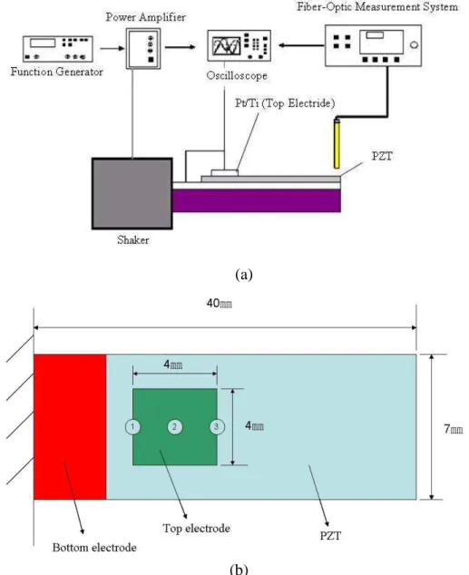
The first step is to demonstrate that the PZT film has sufficient actuation strength to excite the silicon-based structure. The specimen was cut into a beam with the dimensions 40 mm x 7 mm. The top electrode was patterned with dimensions 4 mm x 4 mm. One end of the beam was clamped and the other end was kept free as a cantilever beam. Figure 6(b) presents the top view of the geometry of film and actuated/sensed beam while Fig. 6(a) is the schematic diagram of the experimental setup. The setup consists of a function generator (Motech, FG 503), a power amplifier (Piezotronics, PCB790), a digital oscilloscope (Tektronix, TDS2014) and a fiber-optical measurement system (MTI Instruments, MTI 2000). First, the function generator drove the PZT film with the help of the power amplifier.
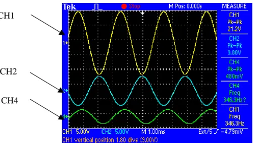
Also, the photonic sensor monitored the vibration of the cantilever. Meanwhile, all of the signals were recorded on a digital oscilloscope, as show in Fig. 7. Figure 7 displays the vibration signals of the beam that was driven by a 6.5µm-thick PZT film with an actuation area of 4 mm by 4 mm. The first trace is the voltage from the function generator which can provide ac voltage between 0 and 10 volts. This electrical signal was amplified 30 times by the power amplifier. The driving signal was divided by 20 before sending to the oscilloscope in order to prevent the damage resulting from the high voltage. The second trace is 1/20th of the driving voltage. The final trace is the signal from the photonic sensor. The system was driven at 346 Hz which was the frequency of the first bending mode.
The vibration amplitude at the tip of the specimen was 2.4 µm at a driving voltage of 196 Vpp.
Furthermore, the frequencies of the vibration and the driving signals were identical to that of the source from the function generator, presented as the first trace. The results displayed in Fig. 7 show that the 4 mm x 4 mm x 6.5 µm PZT film is sufficiently effective as an actuator to drive a 40 mm x 7 mm x 0.5 mm silicon beam with a vibration amplitude of as large as 2.4 µm.
(a)
(b)
Figure 6. (a) Schematic diagram of experimental setup for tests of PZT films and (b) top view of the clamped structure.
Figure 7. Actuation tests of the 6.5 µm-thick PZT film in the first bending mode, using the oscilloscope (CH1: excitation from the function generator; CH2: driving voltage divided by 20; CH4:
vibration signal detected by the photonic sensor).
An actuation linearity test was conducted to determine whether the reverse piezoelectric effect of the film can serve as an actuator. The experimental setup is the same as that in Fig. 6(a), and the recording program LabView was used. The vibration frequency controlled by the function generator was fixed in the first mode of the specimen with an electric field sweeping rate of 1.27 V/µm/s. The applied electric field was from 0 to 12.7 V/µm. The vibration amplitudes at the tip of the specimen were detected by the fiber-optic measure system. Figure 8 presents the experimental results between the amplitude and the applied electric field to the piezoelectric film. Figure 8 reveals that the vibration amplitude is proportional to the applied electric field. Therefore, the film can serve as an actuation source for driving meso- or micro-structures.
y = 0.153x + 0.018 0 0.5 1 1.5 2 2.5 0 2 4 6 8 10 12 14
Electric field (V/um)
A m pl it ud e (u m ) First mode (350.26 Hz) Trend Curve
Figure 8. Actuation linearity testing of PZT films. CH1
CH2
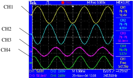
The 6.5-µm thick PZT film adopted in the actuation tests was also used in the sensing tests. The sensing tests were carried out by the function generator, the power amplifier, a shaker (PCB Piezotronics, Inc., AVC-712A01) and the photonic sensor. The shaker served as a vibration source to excite the specimen with the help of the function generator and the power amplifier. The photonic sensor measured the vibration of the specimen at the corner of the free end. The digital oscilloscope recorded the electric signal generated by the PZT film in response to the vibration of the shaker. Figure 9 displays one of the testing results recorded by the oscilloscope. The first trace is the driving voltage from the function generator, which is 10.4 Vpp at 347.7 Hz. The second trace is the driving voltage
from the amplifier into the shaker, divided by a factor of 20. The third trace is the voltage generated by the PZT film in response to the vibration of the specimen. The amplitude is 60 mVpp. The response is
sinusoidal and its frequency is identical to the driving frequency, indicating that the system is in the linear range, and that the PZT film can serve as an effective sensor for small structures. Finally, the final trace is the vibration signal of the cantilever specimen measured by the photonic sensor for reference. It reveals that the photonic signal is 3.12 Vpp, which refers to a vibration amplitude of 7.8
µm. According to the experiments, the frequency of the PZT sensing signal equaled the driving frequency, and the amplitude was proportional to the excitation voltage.
Figure 9. Sensing tests of 6.5 µm-thick PZT film at 347 Hz recorded by the oscilloscope (CH1: excitation from the function generator; CH2: amplified driving signal; CH3: signal of the PZT film;
CH4: reference signal from the photonic sensor).
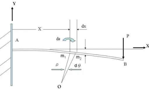
A sensing linearity test was performed to understand whether the piezoelectric effect of the film enables it reliably to serve as a sensor. When a force P is applied, a curvature κ is formed as shown in Fig. 10. Theoretically, the curvature of the cantilever κ is defined as
κ = dθ/ ds (1)
Experimentally, we first denoted three positions along the top electrode as 1, 2 and 3 shown in Fig. 6(b). These points are evenly spaced with distance △x = 2 mm. Then the photonic sensor measured the deflection (w1, w2 and w3) of the cantilever at position 1, 2 and 3. According to Euler-Bernoulli
beam theory, the curvature of the cantilever κ is approximated as κ2 ≈ (w1 -2 w2 + w3) / (△x)
2
(2)
Moreover, the normal strain of the PZT film is ε = κ h/2, where h is the thickness of the cantilever. CH1
CH2 CH3 CH4
Figure 10. Curvature of a bending beam.
Next, the electric voltage applied to the shaker was between 5 and 50 Vpp. The electric signals
generated by the film were measured. The mean and standard deviation of the electric signals were also calculated. Figure 11 shows the relationship between the electric response and the normal strain of the PZT film. The sensing response is proportional to the mechanical deformation of the beam. However, the standard deviation increases with the normal strain.
y = 10.307x - 0.0002 0.00E+00 5.00E-03 1.00E-02 1.50E-02 2.00E-02 2.50E-02 3.00E-02 3.50E-02 4.00E-02 0 0.0005 0.001 0.0015 0.002 0.0025 0.003 0.0035
Normal strain of PZT film
V
ol
t (
V
)
Figure 11. Sensing linearity testing of PZT films.
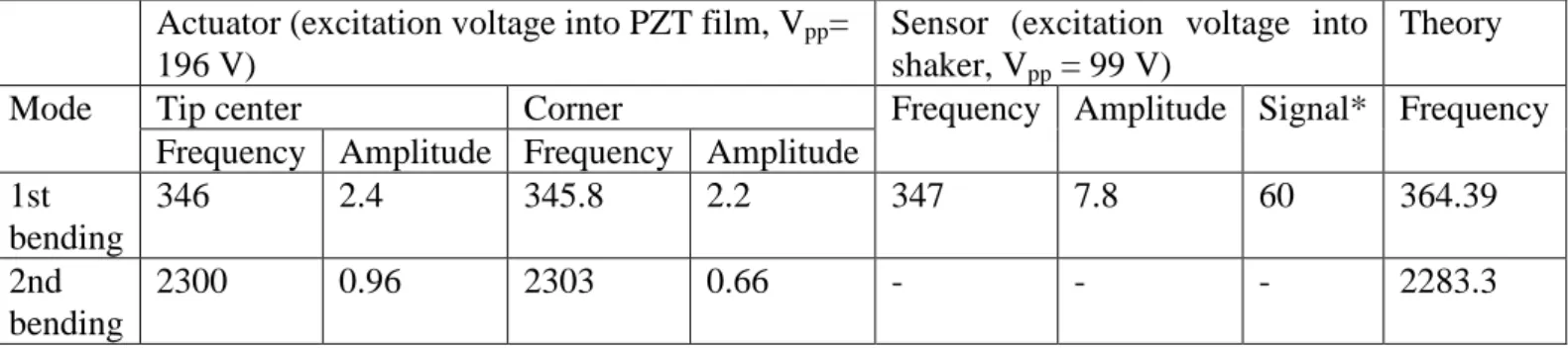
Table 2 summarizes the dynamic tests and theory results of the cantilever specimen. In the actuation tests, the resonance frequencies were measured at the center of the tip and the corner of the beam to identify either a bending mode shown in Fig. 12(a), or torsional vibration mode shown in Fig. 12(b). The frequencies of the first two modes are compared with the theoretical results obtained by Euler-Bernoulli beam theory, suggesting that the experimental results are close to the theoretical values with an error of 5.19 % at the first resonance.
Table 2. Experimental and theoretical results of the vibration of the cantilever specimen. Actuator (excitation voltage into PZT film, Vpp=
196 V)
Sensor (excitation voltage into shaker, Vpp = 99 V)
Theory
Tip center Corner
Mode
Frequency Amplitude Frequency Amplitude
Frequency Amplitude Signal* Frequency 1st bending 346 2.4 345.8 2.2 347 7.8 60 364.39 2nd bending 2300 0.96 2303 0.66 - - - 2283.3
Units: Frequency [Hz], Amplitude [µm]
* The sensing response of the PZT film is in unit of mV.
(a)
(b)
4. Conclusions
PZT films with thicknesses of between 1 and 10 µm were successfully fabricated by the modified sol-gel method using two techniques - precursor concentration modulation and rapid thermal annealing. The thickness of each coating layer was about 0.6 µm, and a 10 µm-thick film was formed by a 16-coating process. The morphology of the films was dense over a crack-free area of as large as 16 mm2. The electrical characteristics were evaluated in terms of dielectric constants and hysteresis curves. The experimental results indicated that the dielectric constant was around 160 at 1 kHz. The remnant polarization and the coercive field of the PZT ferroelectric capacitors are 4.22 µC/cm2 and 6.46 kV/cm, respectively. The dynamic microstructure tests of the PZT films were characterized. The actuation tests demonstrated that a 4 mm x 4 mm x 6.5 µm PZT film drove a 40 mm x 7 mm x 0.5 mm silicon beam as an actuator. Furthermore, the film could generate an electric signal of 60 mVpp as a
sensor while a vibration was input to a shaker. The frequencies of the first two modes of the beam were compared with the theoretical values obtained by Euler-Bernoulli beam theory. This comparison shows that the experimental results are similar to the theoretical results with an error of 5.19 % at the first resonance. The results demonstrated the feasibility of using PZT films fabricated by the modified sol-gel method as actuators and sensors. The next step will be to improve the quality of the films and then investigate the repeatability and reliability of this approach.
Acknowledgements
We gratefully acknowledge the support of this research by the National Science Council grant NSC 92-2218-E-006-103. We thank National Nano Device Laboratories and Center for Micro/Nano Science and Technology, National Cheng Kung University, Tainan, Taiwan for equipment access. Additionally, this work made use of Shared Facilities supported by the Program of Top 100 Universities Advancement, Ministry of Education, Taiwan.
Appendix A. Recipe of PZT sol
1. Dissolve 61.2 g Pb acetate in 38 ml acetic acid.
2. Heat to 110 ◦C (5 min) and then cool to room temperature. 3. Mix 36.9 g Zr n-propoxide with 20.9 ml Ti-isopropoxide. 4. Add to Pb solution the Zr + Ti mixture.
5. Add 40 ml of deionized water. 6. Add 8 ml lactic acid.
7. Add 9 ml glycerol.
8. Add 12 ml ethylene glycol. References
1. Muralt, P.; Kohli, M.; Maeder, T.; Kholkin, A.; Brooks, K.G.; Setter, N.; Luthier, R. Fabrication andcharacterization of PZT thin-film vibrators for micromotors. Sensors and Actuators A 1995, 48, 157-65.
2. Willing, B.; Kohli, M.; Muralt, P.; Setter, N.; Oehler, O. Gas Spectrometry Based on Pyroelectric Thin Film Arrays Integrated on Silicon. Sensors and Actuators A 1998, 66, 109-113.
3. Yang, Z.; Goto, H.; Matsumoto, M.; Maeda, R. Active micromixer for microfluidic systems using PZT-generated ultrasonic vibration. Electrophoresis 2000, 21, 116-119.
4. Kueppers, H.; Leuerer, T.; Schnakenberg, U.; Mokwa, W.; Hoffmann, M.; Schneller, T.; Boettger, U.; Waser, R. PZT thin films for piezoelectric microactuator, applications. Sensors and Actuators A 2002, 97-98, 680-684.
5. Defay, E.; Millon, C.; Malhaire, C.; Barbier, D. PZT thin films integration for the realisation of a high sensitivity pressure microsensor based on a vibrating membrane. Sensors and Actuators A 2002, 99, 64-67.
6. Kanda, T.; Morita, T.; Kurosawa, M.; Higuchi, T. A Rod-shaped vibro touch sensor using PZT thin film. Proceedings of the IEEE Micro Electro Mechanical Systems (MEMS) 1998, 378-383.
7. Hunt, S.; Rudge, A.; Carey, M.; Parfitt, M.; Geoffrey, J.; Huntsman, I. Micro-electro-mechanical-systems direct fluid shear stress sensor arrays for flow control. Smart Materials and Structures 2002, 11, n 4, 617-621.
8. Inoue, N.; Takeuchi, T.; Hayashi, Y. Compositional design of Pb(Zr,Ti)O3 for highly reliable ferroelectric memories. IEEE Transactions on Electron Devices 2002, 49 (9), 1572-1579.
9. Chang, R.-C.; Chu, S.-Y.; Chung, Y.-T. A study of Love wave devices in ZnO/Quartz and ZnO/LiTaO3 structures. Thin Solid Films 2006, 498, 146 -151.
10. Trolier-McKinstry, S.; Muralt, P. Piezoelectric Thin Films for MEMS. Integrated Ferroelectrics, Vol. 17, p 297-307, 1997.
11. Yao, K.; He, X.; Xu, Y.; Chen, M. Screen-printed piezoelectric ceramic thick films with sintering additives introduced through a liquid-phase approach. Sensors and Actuators A 2005, 118 (2), 342-348.
12. Yao, K.; He, X.; Xu, Y.; Chen, M. Piezoelectric ceramic thick films deposited on silicon substrates by screen-printing. Proceedings of SPIE - The International Society for Optical Engineering, Smart Structures and Materials - Smart Electronics, MEMS, BioMEMS, and Nanotechnology 2004, 5389, 108-113.
13. Walter, V. ; Delobelle, P.; Le Moal, P. ; Joseph, E.; Collet, M. A piezo-mechanical characterization of PZT thick films screen-printed on alumina substrate. Sensors and Actuators, A 2002, 96 (2-3), 157-166.
14. Krupanidhi, S.B.; Maffei, N.; Sayer, M.; El-Assal, K.R.F. Magnetron sputtering of ferroelectric PZT films. Ferroelectrics 1983, 51 (1-2), 93-98.
15. Chang, W.L. Comparison of the microstructures and ferroelectric characteristics of sputter deposited PZT films with and without lead or lead oxide for compensation. Ceramics International 2005, 31 (3), 461-468.
16. Cheng, J.; Li, N.; Cross, L.E.; Meng, Z. Self-poling effects in sol-gel derived Pb(Zr1-xTix)O3 thin films. Materials Research Society Symposium – Proceedings 2003, 748, 179-185.
17. Cheng, J.; Meng, Z. Thickness-dependent microstructures and electrical properties of PZT films derived from sol-gel process. Thin Solid Films 2001, 385 (1-2), 5-10.
18. Gerlach, G.; Suchaneck, G.; Koehler, R.; Sandner, T.; Padmini, P.; Krawietz, R.; Pompe, W.; Frey, J.; Jost, O.S. Properties of sputter and sol-gel deposited PZT thin films for sensor and actuator applications: preparation, stress and space charge distribution, self poling. Ferroelectrics 1999, 230, n 1-4, pt 2, 411/109 - 416/114.
19. Hsu, Y.-C.; Wu, C.-C.; Lee, C.-C.; Caoc, G.Z.; Shen, I.Y. Demonstration and characterization of PZT thin-film sensors and actuators for meso- and micro-structures. Sensors and Actuators A 2004, 116, 369-377.
20. Kwon, Y.T.; Lee, W.I.; Kim, C.J.; Yoo, I.K. Novel silicon carbide/polypyrrole composites; preparation and physicochemical properties. Mater. Res. Bull. 1999, 34 (5), 749.
21. Chen, Z.; Yang, C.; Wang, S.; Yang, B. The effects of the PbO content and seeding layers upon the microstructure and orientation of sol-gel derived PZT films. J. Mater. Sci.: Mater. Electron. 2006, 17 (1), 51.
22. Li, J.; Zhang, L.; Yao, X.; Wang, J. A new and rapid heat-treatment process for fabricating lead zirconate titanate thin film. Ceram. Int. 2004, 30 (7), 509.
23. Xie, J.; Hub, M.; Ling, S.-F.; Du, H. Fabrication and characterization of piezoelectric cantilever for micro transducers. Sensors and Actuators A 2006, 126, 182-186.