Design and Implementation of Grid Connection
Photovoltaic Micro Inverter
Wei-Fu Lai, Shih-Ming Chen, Tsorng-Juu Liang,
Kuan-Wen Lee
Green Energy Electronics Research Center (GREERC) Department of Electrical Engineering,
National Cheng-Kung University, Tainan, Taiwan Email: [email protected]
Adrian Ioinovici,
Sun Yat-sen University,Guangzhou, China Email: [email protected]
Abstract—A 200 W photovoltaic (PV) micro inverter is
designed and implemented in this paper. The proposed inverter includes a high step-up DC-DC converter and a SPWM H-bridge inverter. It transfers solar energy into sinusoidal voltage waveform. The operating principles and the steady-state analysis of continuous conduction modes of the high step-up converter are discussed. The DSP controller TMS320LF2407A is used to achieve the system starting check, abnormal state detection, and maximum power point tracking as well as islanding detection. Finally, a prototype circuit with input range from 20 V to 40 V and 220 Vrms / 200 W output is implemented.
I. INTRODUCTION
Conventional photovoltaic (PV) generation system is sourced from several serially connected PV module strings, which provides a sufficiently high voltage which can be converted to electricity through the PV inverter. If there is one or more solar panels in series is/are shaded, changes in output characteristics called 「 shading effect」 will occur [1][2]. Any type of shade such as dust, bird droppings, leaves shade, and building shadows will make the output power of solar power system declined dramatically when shade appears, or even caused the system shut down. The V-I characteristic of the serially connected PV module is shown in Fig.1(a). When one of the PV modules is affected by shade seriously, the output current will decrease immediately and cause the change in output power. It will generate multiple maximum power points and will cause error detection problems. However, when parallel connected PV modules encounter shade, only one maximum power point exists. The MPP detection problem will not happen under the above-mentioned condition, but the output voltage of the module will be too low to transfer energy to grid through the conventional PV inverter, and the large output current will increase the difficulty of system wiring. The V-I characteristic of parallel-connected PV modules are shown in Fig. 1(b). The micro inverter is used for a single PV module [3]. Because low voltage output is inherent in PV module, a
high step-up DC-DC converter is required in the stage before micro inverter. Finally, the solar energy is connected to main grid or electricity through DC-AC inverter. The control circuit not only provides PWM signals to switches of two power stages, but also traces maximum PV module energy as well as real-time grid detection and protection. Fig.2 shows the two-stage micro inverter. The efficiency of conventional boost converter is restricted by duty ratio for higher output voltage. Theoretically, when duty ratio is closed to unity, the voltage gain will be infinity. However, the reverse-recovery loss of the output diode and switching losses are large; the equivalent series resistance (ESR) of capacitors and parasitic resistances of inductor also constrained the voltage gain and efficiency [3]-[6].
(a) (b)
Fig. 1(a). The output characteristics of PV modules connected in series. (b). The output characteristics of PV modules connected in parallel.
Main Grid
High Step-up DC-DC Converter
PV Module
Micro Inverter
Control circuit
DC-AC Inverter
This paper proposes the design and implementation approach of a PV module micro inverter. The module inverter structure is a two-stage system. The first stage is a high step-up high-efficiency DC-DC converter with maximum power point tracking control. The DC-DC converter raises the input low voltage to a high voltage level, and the maximum power point tracking as well as system starting check control are also achieved in this stage. The second stage is a full-bridge inverter. The DC-AC inverter transforms DC voltage from the first stage into sinusoidal voltage waveform for grid connection, and the abnormal state detection and islanding detection control are also achieved in this stage. The DSP controller TMS320LF2407A is used to achieve 1) the system starting check for the initial settings of the inverter; 2) abnormal state detection on various grid conditions; 3) maximum power point tracking algorithm which uses incremental conductance method; the method senses the output voltage and current of the solar panel to determine the duty cycle of the DC converter to be increased or decreased; 4) frequency shift method is chosen for islanding detection; frequency shift method induces some distortion to the output current of the inverter for controller to detect. Finally, a prototype circuit with input range from 20 V to 40 V and 220 VAC / 60 Hz, 200 W output is
implemented to verify the feasibility of this system. The PV module micro inverter structure in this paper is shown in Fig.3. Islanding Detection vpv + -DSP TMS320LF2407A vpv ADC1 ig Vg
ADC3 ADC4 ADC5
ipv Sm Vbus ADC2 Vg S1 S3 S2 S4 ig Lf Cf + -+ -+ -+ -N1 Sm D4 C4 C1 C3 D3 D2 N2 C2 D1 ipv DC-AC inverter S1 S2 S3 S4 Vbus SPWM Signal PWM Signal MPPT PV Module
High Step-up DC-DC Converter Stage
a b
Fig. 3. The PV micro inverter system structure in this paper.
II. DESIGN AND ANALYSIS OF MICRO INVERTER
HARDWARE
A. High step-up DC-DC converter stage
The high step-up DC-DC converter stage using a switched-capacitor DC-DC converter [4] is shown in Fig. 3. It is a DC-DC converter structure with coupled inductor and two pairs of switched capacitor circuits. The converter includes an active switch Sm, diodes D1-D4, capacitors C1
-C4, and a coupled inductor. It uses coupled inductor and
switched capacitor to achieve high step-up voltage ratio. To simplify the analysis, following assumptions are made: 1) all circuit components are ideal except coupled inductor. 2) the value of capacitors C1, C2,C3 , and C4 are large
enough, so the voltage VC1, VC2, VC3 and VC4 can be
considered as constant value. 3) the turn ratio n of dual winding coupled inductor is equal to N2/N1. 4)
the magnetizing inductance Lm is large enough, so the
circuit is operated in continuous condition mode. Fig.4 shows three operating modes in one switching period. The operating modes are described as follows:
Mode I: In this mode, switch Sm is turned on, only diode D3
is conducted. Magnetizing inductor Lm is storing energy
from Vin, and switched capacitors changes their condition
from charging to discharging energy to output. The magnetizing inductance Lm and primary leakage inductance
Lk1 are storing energy from Vin; meanwhile Vin is also
transferred through coupled inductor to secondary winding
N2 and be in series with switched capacitor C1 and C2, and
then their energy is discharged to capacitor C3 and load R.
This mode ends when switch Sm is turned off.
N1 R Vin D2 D3 + _ C3 S1 C4 VO C1 D1 N2 D4 C2 +vLm_Lm LLK1 N1 R Vin + _ C3 S1 C4 VO D4 + + +v Lm Lm_ N1 D2 D3 C1 D1 N2 + + C2 LLK1 + + + + N1 R Vin + _ C3 S1 C4 VO D4 + + +v Lm Lm_ N1 D2 D3 C1 D1 N2 + + C2 LLK1 (a) (b) (c)
Fig. 4 Two operating modes during one switching period at CCM operation. (a) mode I, (b) mode II, (c) mode III.
Mode II: During this transition interval, the Lm is changed
from storing to releasing energy; switched capacitors are also changed from discharging to charging status. Switch Sm,
diodes D1, D2 and D4 are conducted. The leakage energy
charge capacitor C4through diode D4; the Lm is delivering its
energy through coupled inductor to charge capacitor C1 and C2. The mode ends when currents iLK1 decreased to zero.
Mode III: During the interval, The Lm is constantly releasing
its energy to switched capacitors. The Sm, D3, and D4 are off;
diodes D1 and D2 are conducted. The iLm is decreasing
because the magnetizing inductance energy charges capacitor C1 and C2 continuously through the coupled
inductor. The energy stored in capacitor C3 and C4 are
constantly discharged to the load R. This mode ends when switch Sm is turned on at the beginning of the next switching
period.
To simplify the steady state analysis, the leakage inductances at secondary and primary sides are neglected. Using the voltage-second balance principle, the voltage across magnetizing inductor Lm can be written as following:
(
)
∫
DTs +∫
− = 0 Ts DTs in C4 indt V V dt 0 V (1)(
)
∫
DTs + − +∫
= 0 Ts DTs C1 3 C 2 C 1 C V V dt V dt 0 V (2)Arranging equation (1) and (2), the voltage across capacitor C3 and C4 can be shown as:
in 4 C V D 1 1 V − = (3)
(
)
in 2 C 1 C 3 C V D 1 D 1 n D DV V V − + = + = (4)The output voltage VO is the sum of VC3 and VC4. The
voltage gain ratio MCCM can be written as:
(
)
D 1 n D 1 1 V V M in o CCM − + + = = (5)The boundary normalized magnetizing inductor time constant τLmB can be derived as:
. ) Dn n 1 )( n 2 1 ( 2 D) -D(1 τLmB= + + 2+ (6)
Fig.5 shows the voltage gain curve and the boundary normalized magnetizing inductor time constant curve, which are the function of duty ratio at CCM condition when the turns ratio is 5.
Fig. 5. The voltage gain MCCM and boundary normalized magnetizing
inductor time constant τLm versus duty ratio of the proposed converter, n =
5. B. DC-AC Inverter Stage
As shown in Fig. 3,The DC-AC inverter consists of a full bridge inverter comprises of four switches and with a low-pass filter. The hybrid pulse width modulation (HPWM) is used for switch driven [7]. The HPWM method uses two different switching frequency signals to drive switches respectively. There are only two of four switches commuted at lower frequency which is equal to grid frequency. Other two switches are driven by the pulse width modulation signals came from the compared result of sinusoid amplitude signal and triangle carrier. Fig.6(a) shows the HPWM switch driving signals of the full bridge inverter. The operating modes are described as follows:
Mode I: During positive half cycle, switches S1 and S4 are
active; other switches including S2 and S3 are turned off. The
switch S4 is subject to duty cycle modulation control. The
average voltage vab among the points a and b can be derived
as:
bus
ab DV
v = (7)
The D is duty ratio determined by the compared results of the sinusoid amplitude control signal VControl and the
triangle carrier signal VTri. When VTri > VControl, S4 is turned
on, and vice versa. Fig.6(b) shows the HPWM duty cycle modulation control scheme.
Mode II: During negative half cycle, switches S2 and S3 are
active; other switches including S1 and S4 are turned off. The
switches S3 is subject to duty cycle modulation control.
When VTri > VControl, S3 is turned on, the average voltage vab
among the points a and b can be derived as:
bus
ab DV
v =− (8)
The amplitude modulation index ma and frequency
modulation index mf can be written as (9) and (10). The fS is
switching frequency and the fg is the modulation frequency.
Tri ^ Control ^ a V V m = (9) g S f f f m = (10)
Because of upper switches, S1 and S2, are at commuted at
low frequency, the switching losses are significantly reduced than others and the inverter efficiency is then improved [8].
(a)
(b)
Fig. 6 (a) The HPWM signals on the switches of the full-bridge inverter. (b) The HPWM duty cycle modulation control scheme.
III. DESIGN AND SETTING OF MICRO INVERTER
FIRMWARE
There are three major control programs including starting check, system abnormal detection, maximum power point
tracking, and islanding detection in the micro inverter. In the following section, the settings and function will be discussed.
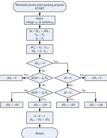
A. Maximum Power Point Tracking Program:
The maximum power point tracking algorithm used in this paper is incremental conductance method [9]-[12]. It senses the PV module output voltage vpv and current ipv to
determine the duty cycle of the DC-DC step-up converter to be increased or decreased. When the sensed voltage is equal to the voltage from the last cycle and the current increment is positive; then the duty cycle will be increased, and vice versa. If the sensed voltage is unequal to the voltage from the last cycle, then the change of duty cycle is based on (11). Fig.7 shows the program flow chart of the maximum power point tracking. dV dI V I − = (11)
B. System Abnormal Protection Program:
Referring to the specification of IEEE Std. 929, the grid voltage range is 88% - 100% of 220 Vrms (194 Vrms – 242
Vrms) and the grid frequency range is 59.3 Hz – 60.5 Hz.
When the system abnormal program detects the voltage vg
constantly out of setting range for more than 330ms, or the frequency fg constantly out of setting range for more than
100ms, the system will be shut down. Fig.8 is the program flow chart of system abnormal detection.
Maximum power point tracking program START
Sense voltage vpv & current ipv
Dk = Dk-1 + ΔDk-1 Vpv = Vk Ipv = Ik dVpv = Vk - Vk-1 dIpv = Ik - Ik-1 dVpv = 0 dI/dV = -Ik/Vk dI/dV > -Ik/Vk dI = 0 dI > 0 ΔDk = +ΔD ΔDk = +ΔD ΔDk = -ΔD ΔDk = 0 k = k + 1 Dk+1 = Dk + ΔDk Return ΔDk = +ΔD Yes Yes Yes Yes Yes No No No No No ΔDk = 0
Fig. 7. Maximum power point tracking program flow chart
< > rms rms g V 196 V 242 v < > Hz 3 . 59 Hz 5 . 60 fg Continue 110ms Continue 330ms Feedback vg, fg System abnormal detection program START Yes Yes Yes Yes No No No No flag_system_start = 0 System shutdown
Fig. 8. Abnormal state detection program flow chart C. Islanding Detection Program:
The islanding detection is the combination of both active and passive methods. The passive method detects the voltage and frequency changing range as system abnormal detection is working. When the islanding occurs but the abnormal phenomena are still within the setting range, passive method cannot detect the abnormal condition; therefore the active method is necessary. The active method adopts frequency shift algorithm, which will deform output current waveform. When islanding is occurred, the output current frequency will be shifted, which can be regarded as grid islanding. The system will be shut down immediately. According to the specification of IEEE Std. 929, the total current distortion should be less than 5% and the period of islanding detection time should be within 2 seconds. When the frequency shift is higher than 10° at positive half cycle and negative half cycle, the islanding is triggered. The system will be shut down by the islanding detection program within 250 ms. Fig.9 is the program flow chart of islanding detection.
IV. EXPERIMENTAL RESULTS
The typical power rating of a crystalline silicon PV module is 180 W–300 W. A 200 W micro inverter prototype with protection and detection functions is presented to verify the practicability of the proposed micro inverter. Circuit specifications are described as follows: Output power PO is
200 W; output voltage VO is 220 VAC; Output frequency fO
is 60 Hz; DC-DC converter output voltage VBUS is 400 V;
Input voltage Vpv is from 20 to 40 V; Switching frequency fm
of Sm is 50 kHz; Switching frequency fs1 of S1 and S2 is 120
Hz and Switching frequency fs2 of S3 and S4 is 18 kHz. With
reference to (5), the turns ratio is given as n = 5 and the duty ratio D is about 0.56 for DC-DC step-up converter. When it operates in CCM at half load, the load resistance R = 1600 Ω substitute into (6), and then the boundary magnetizing inductance of coupled inductor LmB is obtained.
. H 92 . 17 L 00056 . 0 R f L m S mB⋅ > ⇒ > µ (12)
The actual inductance of magnetizing inductor Lm of
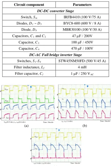
coupled inductor is measured as 18.41 μH and the primary leakage inductance is 0.62 μH. The rest of component parameters are described as follows: For the DC-DC converter stage, Switch Sm is chosen to be IRFB4410 (110
V/ 75A); Diodes D1 ~ D3 is chosen to be BYC8-600 (600V /
8A); Diode D4 is chosen to be MBR30100 (100V / 30A);
Capacitors C1 and C2 are chosen to be 47 µF / 200V;
Capacitor C3 is chosen to be 100 µF / 450V; Capacitor C4 is
chosen to be 470 µF / 100V. For the DC-AC Full-bridge inverter stage, Switches S1 ~ S4 are chosen to be
STW45NM50FD (500V / 45A); Value of filter inductance Lf
is 4 mH and the value of filter capacitor Cf is equal to 1 µF /
250 VAC. The switching signals and program execution are all are provided by TMS320LF2407A, which is a well-known 16 bits digital signal processor.
TABLEI.CIRCUIT SPECIFICATIONS
Item Specification
Output power, Po 200 W
Output voltage, Vo 220 VAC
Output frequency, fo 60 Hz
DC-DC converter output voltage, VBus 400 V
Input voltage, Vpv 20 ~ 40 V
Switching frequency fm of Sm 50 kHz
Switching frequency fs1 of S1 and S2 120 Hz
Switching frequency fs2 of S3 and S4 18 kHz
Fig. 10 shows the major waveforms of the high step-up DC-DC converter at full load output of 200 W. The peak voltage across switch Sm has been constrained under 100V,
which is shown in Fig.10(a). The diode D1 and D2 are
parallel when capacitors are under charging period. Fig. 10(b) shows the capacitors C1 and C2 charging current, and its
inrush current has been constrained. Fig.10(c) reveals the leakage inductance energy can be recycled through D4 to C4.
Fig. 11(a) is the four switch driving signals of DC-AC full-
bridge inverter. Fig. 11(b) is the output voltage and current waveform when the inverter is connected to grid. These waveforms are agreed with the simulation results and design parameters.
TABLEII. PART NUMBER OF MAJOR COMPONENTS
Circuit component Parameters DC-DC converter Stage Switch, Sm IRFB4410 (100 V/75 A) Diodes, D1 ~ D3 BYC8-600 (600 V / 8 A) Diode, D4 MBR30100 (100 V/30 A) Capacitors, C1 and C2 47 µF / 200V Capacitor, C3 100 μF / 450V Capacitor, C4 470 μF / 100V
DC-AC Full bridge inverter Stage
Switches, S1-S4 STW45NM50FD (500 V/45 A)
Filter inductance, Lf 4 mH
Filter capacitor, Cf 1 µF / 250 VAC
Time: 10us/div VDS(50 V/div), iin, iDS(20 A/div) vGS vDS iin iDS Time: 10us/div iD1, iD2 (1 A/div) vGS iD1 iD2 (a) (b) Time: 10us/div iD3(1 A/div), iD4(10 A/div) iD3 iD4 vGS (c)
Fig. 10. Major waveforms of the high step-up DC-DC converter stage at
full load 200 W output. (a) vDS, iin, iDS. (b) iD1, iD2. (c) iD3, iD4.
Time: 5 ms/div vgs1, vgs2, vgs3, vgs4 (20 V/div) S2 S3 S4 S1 Time: 5 ms/div vg(100 V/div), ig(1 A/div) vg ig (a) (b)
Fig. 11. (a) Four driving signals of switches of the DC-AC inverter. (b) Output voltage and current waveforms as the inverter is connected to grid.
The Fig.12-14 shows the measured results of proposed detection and protection programs. Fig. 12 is the tracking waveforms of the maximum power point tracking. The PV power simulation facility is Agilent E4360A solar power simulator. The simulator setting parameters are 1) open circuit voltage 33.2 V, 2) short circuit current 8.58 A, 3)
maximum power point voltage 26.6 V, and 4) maximum output current 7.9 A, which are cited from a real PV module. Fig. 12(a) is the tracking record waveforms when the simulator output power is 200 W at the startup of the proposed inverter. Fig. 12(b) is the tracking curves depicts the maximum power point changing from 200 W down to 100 W. The program tracing time is about 400 ms. The MPPT accuracy is defined as:
% 100 P P MPPT Set Trace % = ⋅ (13)
The PTrace means the power which has been traced by
inverter when MPPT function is active. Pset is the
maximum power point. The MPPT accuracy is above 95 %.
Time: 200 ms/div
ppv(100 W/div), vpv(10 V/div), ipv(4 A/div)
ppv
vpv
ipv
Time: 200 ms/div ppv(100 W/div), vpv(10 V/div), ipv(4 A/div)
ppv
vpv
ipv
(a) (b)
Fig. 12.Themeasurement waveforms of the maximum power point
tracking. (a) Maximum power point is 200 W under system start up condition. (b) Maximum power point changing from 200 W to 100 W.
The system abnormal protection verification results are depicted in Fig.13 when grid voltage is out of the rated range,which is 194 VAC – 242 VAC, or the grid frequency is
out of rated range, which is 59.3 Hz – 60.5 Hz. Fig. 13(a) illustrates that the system is shut down when the grid voltage is over 242 VAC after 728 ms processing time. Fig.
13(b) shows the system output voltage and current waveforms when the grid voltage is under 196 VAC, and the
system is shut down after 696 ms. Fig. 13(c) shows the measured waveforms when the grid frequency is over 60.5 Hz, and the system will be shut down after 150 ms. Fig. 13(d) shows the measured waveforms when the grid frequency is lower than 59.3 Hz, and the system will be shut down after 186 ms. These results show that the abnormal conditions are detected successfully and the system can be shut down within 1 s.
When islanding is occurred or the power grid is disconnected, the islanding protection program will be activated. Fig. 14(a) shows the phase shift scheme when the islanding detection program is activated, and the current waveform will be shifted 556 μs. Fig. 14(b) shows the system is shut down after islanding occurred, and the detecting duration is about 308 ms. Finally, the highest efficiency of the high step-up DC-DC converter stage is about 96 %, and the measured system efficiency of the proposed micro inverter at full load operation is about 86 %.
Time: 200 ms/div vg(200 V/div), ig(1 A/div)
728 ms
vg
ig
vtrigger System shutdown
Time: 200 ms/div vg(200 V/div), ig(1 A/div) 696 ms vg ig vtrigger System shutdown (a) (b) Time: 20 ms/div vg(200 V/div), ig(1 A/div) 150 ms vg ig vtrigger System Shutdown Time: 20 ms/div vg(200 V/div), ig(1 A/div) 186 ms vg ig vtrigger System Shutdown (c) (d)
Fig. 13. Measured results of the system when abnormal detection program is activated. (a) The grid voltage is over 242 V. (b) The grid voltage is
under 196 V. (c) The grid frequency is over 60.5 Hz. (d) The grid frequency is under 59.3 Hz.
vg(100 V/div), ig(1 A/div) Time: 2 ms/div 556 us
vg
ig
The signal of power grid disconnecting 308 ms
vg(100 V/div), ig(1 A/div) Time: 50 ms/div
vg ig
(a) (b)
Fig. 14.Measured waveforms of islanding detection. (a) Phase shift
diagram when islanding detection program is activated. (b) System output voltage and current waveforms when the simulated power grid is cut off.
V. CONCLUSION
A PV micro inverter has been designed, implemented and verified in this paper. The major difference between conventional PV inverter and the proposed micro inverter is the ability to raise the input voltage. The proposed micro inverter can efficiently raises the input voltage to the level that can be transformed to electricity. It also embedded with MPPT, system abnormal protection, and anti-islanding features; they are designed for harvesting maximum solar power from the PV module and preventing any abnormal situations occurred. Finally, a prototype micro inverter with input range from 20 V to 40 V and 220 VAC / 200 W output
is implemented. The DSP controller is TMS320LF2407A. The MPPT accuracy is higher than 95 %. The system abnormal protection and islanding detection are successfully activated and the system can be shut down within 1 second. The highest efficiency of the high step-up converter is 96 % at 100 W output. The highest efficiency of the overall system is 86 %.
ACKNOWLEDGMENT
The authors gratefully acknowledge financial support from the Bureau of Energy, Ministry of Economic Affairs, Taiwan, project No. 101-D0204-2, and National Science Council of Taiwan under project No. NSC 100-2218-E-006-002.
REFERENCES
[1] R. Ramaprabha, B. Mathur, M. Murthy, and S. Madhumitha, “New Configuration of Solar Photo Voltaic Array to Address Partial Shaded Conditions,” International Conference on Emerging Trends in
Engineering and Technology, pp. 328 - 333, 2010.
[2] Q. Zhang, X. Sun, Y. Zhong, and M. Matsui, “A Novel Topology for Solving the Partial Shading Problem in Photovoltaic Power Generation System,” Power Electronics and Motion Control
Conference, pp. 2130 - 2135, 2009.
[3] S. M. Chen, T. J. Liang, L. S. Yang, and J. F. Chen, “A Cascaded High Step-up DC-DC Converter with Single Switch for Microsource Applications,” IEEE Trans. Power Electron., vol. 26, no. 4, pp. 1146-1153, Apr. 2011.
[4] T. J. Liang; S. M. Chen; L. S. Yang; J. F. Chen; Adrian Ioinovici, , “Ultra Large Gain Step-up Switched-Capacitor DC-DC Converter with Coupled Inductor for Alternative Sources of Energy,” IEEE
Trans. Circuits Syst. I, Reg. Papers, to be published.
[5] T. J. Liang, S. M. Chen, L. S. Yang, J. F. Chen, A. Ioinovici, “A single switch boost-flyback DC-DC converter integrated with switched-capacitor cell,” in Proc. IEEE. ICPE & ECCE, 2011, pp. 2782-2787.
[6] W. Li and X. He, “Review of Non-isolated High-Step-Up DC/DC Converters in Photovoltaic Grid-Connected Applications” IEEE
Trans. Ind. Electron., vol. 58, no. 4, pp. 1239–1250, Mar. 2011.
[7] T. H. Ai, J. F. Chen, and T. J. Liang, "A random switching method for HPWM full-bridge inverter," IEEE Trans. on Ind. Electron., vol. 49, no. 3, pp. 595-597, Jun. 2002.
[8] R. S. Lai and K.D.T. Ngo, "A PWM method for reduction of switching loss in a full-bridge inverter," IEEE Trans. on Power
Electron., vol. 10, no. 3, pp. 326-332, May 1995.
[9] P. Midya, P. T. Krein, R. J. Turnbull, R. Reppa, and J. Kimball, "Dynamic maximum power point tracker for photovoltaic applications," in Proc. IEEE PESC, vol. 2, pp. 1710-1716, Jun. 1996. [10] J. H. R. Enslin, "Maximum power point tracking: a cost saving
necessity in solar energy systems," in Proc. IEEE IECON, pp. 1073-1077, Nov. 1990.
[11] K. Harada and G. Zhao, "Controlled power interface between solar cells and AC source," IEEE Trans. on Power Electron., vol. 8, no. 4, pp. 654-662, Oct. 1993.
[12] R. Panda and R. K. Tripathi, "A novel sine wave inverter with PWM DC link," in Proc. IEEE. ICIINFS, pp. 1-5, Dec. 2008.