碩士論文
Graduate Institute of Electronics Engineering College of Electrical Engineering and Computer Science
National Taiwan University Master Thesis
整合扇出型晶圓尺寸封裝設計之繞線系統
A Redistribution Layer Routing System for Integrated Fan-Out Wafer-Level Chip-Scale Packages
林柏僑 Bo-Qiao Lin
指導教授:張耀文 博士 Advisor: Yao-Wen Chang, Ph.D.
中華民國 105 年 6 月
I would like to express my gratitude to my advisor, Professor Yao-Wen Chang, for his tremendous advice, instruction, and guidance throughout my pursuit of the Master’s degree. I learned many important things from him, including research methodologies, presentation skills, technical writing, and the right attitudes toward things, especially for the importance of integrity, commitment, and priority setting.
Besides, I greatly appreciate the committee members of my oral defense, Professor Hung-Ming Chen, Professor Shao-Yun Fang, and Professor Ting-Chi Wang for their valuable comments and suggestions.
I am grateful to every member of the Electronic Design Automation Lab- oratory in National Taiwan University for many inspiring discussions and useful comments on my research. Especially, I would like to thank I-Peng Wu for his friendship and assistance with my research.
My deepest appreciation goes to my dear parents. Without their constant support and endless love, the completion of this thesis would not have been possible.
Bo-Qiao Lin
National Taiwan University June 2016
研究生:林柏僑 指導教授:張耀文 博士
國立臺灣大學電子工程學研究所 摘要
整合扇出型晶圓尺寸封裝 (integrated fan-out wafer-level chip-scale package) 是一個新興的封裝技術,此封裝技術通常會藉由多層重分佈 層 (redistribution layer) 來進行多個晶片間的訊號傳輸。目前尚未有發 表的論文是針對整合扇出型晶圓尺寸封裝的重分佈層繞線做探討,大 部分相關的發表論文著重於考慮覆晶 (flip-chip) 封裝上的重分佈層繞 線問題,傳統的覆晶封裝中通常只有單一個晶片,而覆晶封裝上的重 分佈層繞線問題可以分為三類,分別是自由配對繞線問題、非自由配 對繞線問題與混合型配對繞線問題。由於整合扇出型晶圓尺寸封裝整 合了多個晶片,相關的繞線器無法有效地處理此技術的重分佈層繞線 問題。為了彌補相關論文缺乏對於多個晶片及多層重分佈層的考慮,
我們提出了一個新的整合扇出型晶圓尺寸封裝中的重分佈層繞線問題,
此問題考慮到了訊號的完整性、訊號線的分層、重分佈層數量的最小
法。我們提出了一個同心圓模型 (concentric-circle model) 來模擬一個 晶片跟其他所有晶片之間的連線,基於此模型,我們將晶片之間的連 線分配到適當的重分佈層來避免訊號線過長。除此之外,此模型將晶 片間非自由配對連線的幾合資訊整合到了一個網路流模型,此網路流 模型可以產生在扇出區域中的繞線雛型。實驗結果顯示我們的演算法 的高品質與高效率。
關鍵詞:實體設計、整合扇出型晶圓尺寸封裝、重分佈層、重分佈層
繞線
PACKAGES
Student: Bo-Qiao Lin Advisor: Dr. Yao-Wen Chang
Graduate Institute of Electronics Engineering National Taiwan University
Abstract
The integrated fan-out (InFO) wafer-level chip-scale package (WLCSP) is an emerging packaging technology, which typically consists of multiple redistribu- tion layers (RDLs) for signal redistributions among multiple chips. There is still no published work specifically on the RDL routing for the InFO WLCSP. Published RDL routing works consider different types of RDL routing for flip-chip packages, namely free-assignment, pre-assignment, and unified-assignment routing, for a sin- gle chip. With the integration of multiple chips under the InFO WLCSP, however, previous works cannot achieve high efficiency and effectiveness with simple exten- sions. To remedy the deficiencies of poor interactions between chips and multiple RDLs, we formulate a new RDL routing problem for the InFO WLCSP and present the first work in the literature to handle the unified-assignment, multi-layer multi- chip RDL routing problem (without RDL vias), considering signal integrity, layer assignment, layer number minimization, and total wirelength minimization. We propose a concentric-circle model which models all the connections among one chip
and appropriate layers to avoid long detours. In addition, this model transforms the geometrical information of the pre-assignment connections among chips into a network-flow model to generate a routing prototype in a fan-out region not covered by any chip efficiently and effectively. Experimental results demonstrate the high quality and efficiency of our algorithm.
Keywords: Physical Design, Integrated Fan-Out Wafer-Level Chip-Scale Package, Redistribution Layer, RDL Routing
Acknowledgements iii
Abstract (Chinese) iv
Abstract vi
List of Tables x
List of Figures xi
Chapter 1. Introduction 1
1.1 Integrated Fan-Out Wafer-Level Chip-Scale Packages . . . 1
1.2 Classification of RDL Routing Problems for Traditional Flip-Chip Pack- ages . . . 4
1.3 Related Works . . . 7
1.3.1 RDL Routing for the Free-Assignment Routing Problem . . . 7
1.3.1.1 Network-Flow-Based Methods . . . 7
1.3.1.2 Non-Network-Flow-Based Methods . . . 10
1.3.2 RDL Routing for the Pre-Assignment Routing Problem . . . 10
1.3.2.1 ILP-Based Methods . . . 10
1.3.2.2 Non-ILP-Based Methods . . . 11
1.3.3 RDL Routing for the Unified-Assignment Routing Problem . . . . 11
1.4 Motivation . . . 12
1.5 Our Contributions . . . 13
1.6 Thesis Organization . . . 15
2.2 Layout Constraints of Our Problem . . . 19
Chapter 3. An RDL Routing Algorithm 22 3.1 Algorithm Overview . . . 22
3.2 Layer Assignment for Pre-Assignment Nets . . . 23
3.2.1 Concentric-Circle Model . . . 24
3.2.2 Construction of the Model for Layer Assignment for Pre-Assignment Nets . . . 26
3.2.3 Algorithm Based on the Model . . . 27
3.3 Congestion-Aware Escape Routing for All Chips . . . 31
3.4 Pad/Layer Assignment for Free-Assignment Nets . . . 35
3.5 Outward Ring-by-Ring Routing . . . 39
Chapter 4. Experimental Results 43 4.1 Experimental Setup . . . 43
4.2 Experimental Results and Comparisons . . . 44
Chapter 5. Conclusions and Future Work 49
Bibliography 53
Publication List 58
4.1 Benchmark circuit statistics. “#Chips”, “#I/O Pads”, “#Bump Pads”, and “#Pre-Assignment Nets” denote the numbers of chips, I/O pads, bump pads, and pre-assignment nets, respectively. . . 43 4.2 Comparisons of RDL routing results (“N/A”: incomplete routing re-
sults). . . 45 4.3 Runtime analysis. This table shows the runtime of the four stages in
our global routing algorithm. The second and third stages take up the majority portion of the runtime. . . 48
1.1 (a) The cross view of a traditional flip-chip package [15]. (b) The cross view of a multi-chip InFO WLCSP. . . 3 1.2 RDL structure comparisons of traditional flip-chip packages and an
InFO WLCSP. (a) The RDL structure of a peripheral-I/O flip-chip package without a fan-out region. (b) The RDL structure of an area- I/O flip-chip package without a fan-out region. (c) The RDL struc- ture of a multi-chip InFO WLCSP with two RDLs. . . 5 1.3 Classification of RDL routing problems for traditional flip-chip pack-
ages according to the RDL structures and assignment types between I/O pads and bump pads [15]. . . 6 1.4 An example flow network construction [8, 9]. (a) Construction of tile
and intermediate nodes. (b) The flow network of an RDL. Nodes s and t are the source and sink, respectively. Note that the sink is connected from all bump pads; only three edges from bump pads to the sink are shown here for brevity. . . 8 1.5 Comparisons of the previous work [10] with extensions and our al-
gorithm. (a)–(b) A two-layer routing result with detours, generated from the previous work [10] with the extension that modifies a flow network in [10] for multiple layers by duplicating the vertices and edges of the original network for each layer. The detours are caused by two reasons: (1) its congestion estimation does not consider pre- assignment nets, and (2) there exist net ordering problems for pre- assignment nets. (c)–(d) A better two-layer routing solution from our algorithm. . . 14 2.1 (a) The structure of the addressed RDL routing plane. Multiple chips
are integrated into a single layout, and some pre-assignment nets need to be electrically connected in the final layout. Besides, each free-assignment I/O pad should be connected to a bump pad. (b) A single-layer routing result satisfying all the design rules corresponding to (a). . . 18
net segments in both the fan-in region (the region occupied by I/O pads is excluded) and the fan-out region. (b) Violation of the non- detour-around-boundary constraint: the routed net detouring around a large portion of the chip boundaries is not allowed. (c) Violation of the routing-angle constraint: the angle between two routing segments should be 90◦ or 135◦. . . 20 3.1 Overview of our proposed routing algorithm. . . 23 3.2 (a) An RDL layout with three chips and multiple pre-assignment nets.
The blue arcs indicate the orders of corresponding nodes of I/O pads that appear on our concentric-circle model. (b) The corresponding concentric-circle model of (a). The inner circle represents the leftmost chip in (a), and the outer circle represents the neighboring geometry of the leftmost chip. The red arcs correspond to the pre-assignment nets connecting the nodes which represent the pre-assignment I/O pads. (c) A sample solution of the layer-assignment problem. The nets of the same color are assigned to the same layer. . . 25 3.3 An example of our concentric-circle model in layer assignment for pre-
assignment nets. (a) The same concentric-circle model as Figure 3.2 with a cutting bond. (b) The LCS problem converted from (a). The upper (lower) line corresponds to the inner (outer) circle in (a), and the nodes on the upper (lower) line follow the same order as on the inner (outer) circle, starting from the cutting bond counter-clockwise.
(c) Candidate locations for a cutting bond on an inner (outer) circle denoted in solid black arcs. If any two bonds intersect, some degree intervals on the two circles are excluded from consideration because no cutting bond will co-exist with an intersection. . . 28 3.4 The layer assignment algorithm for pre-assignment nets. . . 30 3.5 The network flow model inside a tile with four bump pads proposed
by [29]. . . 32 3.6 An example of the flow network of one chip. By adjusting the bound-
ary capacities of the flow network according to (1) the resulting cost of a bipartite matching and (2) the locations of pre-assignment I/O pads, we can achieve a good distribution of nets after escape routing considering the congestion of the whole layout. . . 33
pre-assignment nets. q11 is the I/O pad of consideration, and bo1, bo2, and bo3 are the candidate bump pads to be connected to. The to-be- checked regions are constructed from the perspective of the leftmost chip based on the pre-assignment nets connecting to it. (b) The cor- responding concentric-circle model of (a). The inner circle represents the leftmost chip in (a). The red and blue arcs are the degree inter- vals derived from the layout. Starting from q11, the red ones are the ones that need to be checked whether a potential detour may occur because they overlap with the bottom to-be-checked region, whereas the blue one needs not be checked. . . 37 3.8 Assume there is a crossing consisting of edges (the solid lines) at
the layer l1 in an MCMF result, and there are an edge between qaj and boe at the layer l2 and an edge between qjb and bof at the layer l3. This contradicts the fact that the total cost of the MCMF result is minimum. . . 38 3.9 An example for our outward ring-by-ring routing algorithm. (a) The
global routing result with two types of violations after finishing the first ring. All the I/O pads are assigned to correct ring passing points on the first ring. The ring passing points on the first ring are con- nected to the targets. (b) The global routing result after finishing the second ring. All the violations in (a) are corrected by reassigning some I/O pads to bump pads or detouring the pre-assignment net. . 41 3.10 The global routing algorithm. . . 42 4.1 The routing solution of info3 on the first layer. The red lines are the
pre-assignment nets, and the black lines are the free-assignment ones. 46 4.2 The routing solution of info3 on the second layer. The red lines are
the pre-assignment nets, and the black lines are the free-assignment ones. . . 47 5.1 Comparisons of the traditional package on package (PoP) technology
and the PoP with InFO WLCSPs [2]. The PoP with InFO WLCSPs does not need a substrate and can obtain a thinner package thickness.
Through mold vias (TMVs) are used to connect the packages. . . 51
decides the locations of the chips in a package. We might also need to handle I/O buffer placement. The overall target is connecting each I/O buffer in a package to the corresponding pin (the other components in this figure). . . 52
Introduction
In this thesis, we propose a redistribution layer (RDL) routing algorithm to min- imize the wirelength and the number of RDLs considering signal integrity. In the following sections, we first introduce the integrated fan-out (InFO) wafer-level chip- scale package (WLCSP) in Section 1.1. Then, we introduce traditional RDL routing problems in Section 1.2. Next, a survey of related works is given in Section 1.3. Af- ter that, we explain our motivation in Section 1.4 and summarize our contributions in Section 1.5. Finally, in Section 1.6, we show the organization of the rest of this thesis.
1.1 Integrated Fan-Out Wafer-Level Chip-Scale Packages
The traditional flip-chip package is a technology for connecting a chip to an external circuitry such as package carriers. A chip is flipped over and mounted on a package carrier, as shown in Figure 1.1(a). To ease design changes, an extra metal layer, called a redistribution layer (RDL), is added and used to redistribute nets between I/O pads in a chip and bump pads in a package carrier. The RDL routing problem is to redistribute and connect nets between I/O pads and bump pads.
However, with the increasing design complexity, many advanced packaging technologies have been proposed for system integration recently. Among these ad-
vanced packaging technologies, the integrated fan-out (InFO) wafer-level chip-scale package (WLCSP) [2, 19, 30] provides a promising alternative with a small form fac- tor, a better signal-to-noise ratio, and improved thermal characteristics. A multi- chip InFO WLCSP uses micro-bumps and redistribution layers (RDLs) to connect neighboring chips [2, 12]. As illustrated in Figure 1.1(b), RDLs are the top metal layers of a chip, and multiple chips share the same RDLs in a multi-chip InFO WLCSP.
In modern IC designs, I/O pads are usually placed along the boundaries of chips, called peripheral I/Os, and the RDLs are used to redistribute I/O pads to bump pads or connect I/O pads among different chips. Accordingly, an RDL router is needed to connect I/O pads to the I/O pads in other chips or the bump pads in the same chip or the fan-out region not covered by any chip. RDLs under a multi- chip InFO WLCSP are divided into two regions: (1) the fan-in region, which is the region directly underneath chips, and (2) the fan-out region, which is the region that does not belong to the fan-in region. Therefore, I/O pads can be redistributed to the fan-out region outside the chips to increase the pin count. Moreover, passive devices such as inductors and capacitors can be formed over molding compound for lower substrate loss and higher electrical performance [19]. Molding compound also provides physical protection for the chips.
Figures 1.2(a) and (b) show two typical RDL structures for traditional flip- chip packages. In a traditional flip-chip package, only a single chip is in the package, and there is usually only one RDL. Figure 1.2(c) shows the multi-layer RDL struc- ture of a multi-chip InFO WLCSP. Different from the RDL structures of previous works, there are multiple chips and multiple layers. Besides, the types of connec- tions are different. In addition to the original free-assignment connections, which connect I/O pads to bump pads to transmit signals into or out of a package, another
(a)
(b)
chip1 chip2
molding compound
RDLs micro-bump
top metal layer redistribution layer
package carrier metal 1 cells and I/O buffers
I/O pad
bump pad bump ball isolator chip
(flipped over)
Figure 1.1: (a) The cross view of a traditional flip-chip package [15]. (b) The cross view of a multi-chip InFO WLCSP.
type of connections under a multi-chip InFO WLCSP connects two I/O pads of dif- ferent chips to directly transmit signals. In this addressed problem, the connections between I/O pads are predefined because the functions of I/O pads are typically predefined by IC designers.
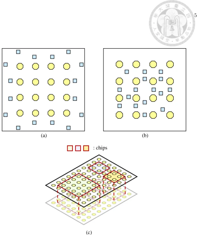
1.2 Classification of RDL Routing Problems for Traditional Flip-Chip Packages
In a traditional flip-chip package, only a single chip is in the package, and there is usually only one RDL. According to the RDL structures, the flip-chip pack- ages can be categorized into two types: (1) the peripheral-I/O flip-chip package and (2) the area-I/O flip-chip package, as shown in Figures 1.2(a) and (b). Gener- ally speaking, the routing for the area-I/O flip-chip package is harder than that for the peripheral-I/O one since the routing region among bump pads in an area-I/O flip-chip package is more congested. On the other hand, the area-I/O flip-chip pack- age exhibits significant advantages in shorter connection wirelength, higher design flexibility, etc.
Depending on the interactions among IC, packaging, and PCB designers, there are three types of RDL routing for traditional flip-chip packages: (1) the free-assignment (FA, for short) routing, (2) the pre-assignment (PA) routing, and (3) the unified-assignment (UA) routing [15]. For the free-assignment routing, the assignment between I/O pads and bump pads are not predefined by designers. For the pre-assignment, in contrast, connections between I/O pads and bump pads are predefined by designers. For the unified-assignment, some connections between I/O pads and bump pads are predefined while the others are not.
There is a series of related works on the RDL routing problems for traditional flip-chip designs. Figure 1.3 shows the classification of RDL routing problems for
(a) (b)
(c)
: chips
Figure 1.2: RDL structure comparisons of traditional flip-chip packages and an InFO WLCSP. (a) The RDL structure of a peripheral-I/O flip-chip package without a fan-out region. (b) The RDL structure of an area-I/O flip-chip package without a fan-out region. (c) The RDL structure of a multi-chip InFO WLCSP with two RDLs.
traditional flip-chip packages according to the RDL structures and assignment types between I/O pads and bump pads. In the next section, we detail the related works shown in Figure 1.3.
Peripheral-I/O, free-assignment Fang et al., ICCAD’05: Flow Liu et al., DAC’10: VD+Flow
Peripheral-I/O, pre-assignment Fang et al., DAC’07: ILP Lee et al., ICCAD’09: DP Yan and Chen, GLSVLSI’09:
Greedy
Area-I/O, free-assignment
Fang and Chang, ICCAD’08: Flow Yan and Chen, ASPDAC’09: VD
Area-I/O, pre-assignment
Yan and Chen, ICCD’11: Greedy FA
Peripheral-I/O
Area I/O
PA
Area-I/O, unified FA/PA Fang et al., DAC’09: VD+Flow Obstacle-aware
Lee et al., DAC’12: Flow
Figure 1.3: Classification of RDL routing problems for traditional flip-chip packages according to the RDL structures and assignment types between I/O pads and bump pads [15].
1.3 Related Works
In this section, we introduce RDL routing techniques for free-assignment (FA), pre-assignment (PA), and unified-assignment (UA) routing problems for tra- ditional flip-chip packages.
1.3.1 RDL Routing for the Free-Assignment Routing Problem
Most published works utilize network-flow-based algorithms to handle the FA routing problem because each I/O pad can be assigned to any bump pad. The methods can be classified into two types, network-flow-based methods [4, 5, 8, 9, 11, 17, 20] and non-network-flow-based methods [26].
1.3.1.1 Network-Flow-Based Methods
The basic idea is to construct a flow network to model the layout topology, apply a minimum-cost maximum-flow (MCMF) algorithm, and convert the resulting flow solution to a global-routing topology. Finally, a detailed routing algorithm is then applied to assign tracks and determine the actual position for each net.
Fang et al. [8,9] addressed the FA routing problem for peripheral-I/O flip-chip packages and proposed a network-flow-based algorithm to derive a global-routing topology. In this work, a tile is a rectangular region bounded by four bump pads and/or I/O pads, and an interval is a segment between two adjacent bump pads or I/O pads. Based on these tiles, intervals, I/O pads and bump pads, a flow network is constructed for the MCMF algorithm, as shown in Figure 1.4. To control the congestion, each tile (intermediate) node is assigned the capacity of the maximum number of nets that can pass through the corresponding tile (interval) simultane- ously. With the capacity constraints of tile and intermediate nodes, it is guaranteed that the global-routing solution can be transformed into a detailed-routing solution
s
t : bump pad
: I/O pad
: intermediate node : tile node
(a) (b)
Figure 1.4: An example flow network construction [8, 9]. (a) Construction of tile and intermediate nodes. (b) The flow network of an RDL. Nodes s and t are the source and sink, respectively. Note that the sink is connected from all bump pads;
only three edges from bump pads to the sink are shown here for brevity.
without violating design rules. The cost of an edge is set to be proportional to the Manhattan wirelength of this edge. Consequently, minimizing the total cost would lead to shorter total wirelength.
Lee et al. [17] also addressed the FA routing problem for peripheral-I/O flip-chip packages. Besides, they considered obstacles on the RDL layout. They also adopted a network-flow-based algorithm. However, with the obstacles, they constructed a different flow network from the one in [8, 9]. They modified the tile model proposed in [29] to construct a flow network to well consider obstacles.
Liu et al. [20] presented an approach to handling the peripheral-I/O FA routing problem. Based on Delaunay Triangulation (DT) and Voronoi Diagram (VD), they create a flow network with triangular tiles for the MCMF algorithm.
We first introduce DT and VD. Given a set of points P , DT triangulates the plane according to P by a computational geometry technique. A property of DT is that no point lies inside the circumcircle of another triangle. Besides, the minimum angle of all the angles of the triangles is maximized. Also given P = {p1, ..., pn}, VD is a decomposition of a plane into Voronoi cells C = {c1, ..., cn}, such that any point inside ci is closer to pi than any other pj ∈ P, i 6= j. VD can be directly derived through DT because VD is the dual graph of DT. The work first computed the DT and VD based on the set of points induced from bump pads, I/O pads, and some control points on the boundary of a chip. They then used VD as the flow network, and flow edges are constructed between VD nodes and pads. The cost of an edge is decided by its wirelength, and the capacity of edges connecting source (sink) is set to one so that only one net can be attached to one bump or I/O pad. The cost of a VD edge is proportional to the length of the corresponding edge in the dual graph DT. The capacity of the edge connecting a VD node and its neighbor is set according to the length of the common edge of the two DT triangles containing the
VD nodes.
Fang and Chang [4, 5] proposed the first work on area-I/O FA routing prob- lem. Because I/O pads are located everywhere on RDLs, the rectangular tile model proposed in [8, 9] is not applicable. According to the distribution of I/O pads, they modified the flow network and the tile node capacity of the model to deal with the area-I/O flip-chip packages.
1.3.1.2 Non-Network-Flow-Based Methods
Yan and Chen [26] proposed a non-network-flow-based algorithm for the area- I/O FA routing problem. Based on DT and VD, they assigned I/O pads to bump pads iteratively. VD, which is constructed based on all unassigned I/O pads, is applied to perform the assignment in each iteration. After the procedure, they adjust the initial assignment by exchanging assignment pairs to reduce wirelength and remove crossing pairs.
1.3.2 RDL Routing for the Pre-Assignment Routing Problem
The network-flow-based methods are not applicable because each I/O pad must be connected to the predefined bump pad, which violates the nature of flows in a flow network. Published works for this problem can be categorized into two types, ILP-based methods [6, 7] and non-ILP-based methods [16, 18, 27, 28].
1.3.2.1 ILP-Based Methods
Fang et al. [6, 7] proposed an approach for the peripheral-I/O PA routing problem. They construct an ILP network with the same definition of tiles and in- tervals as [8, 9]. Based on the ILP network, they derive an ILP formulation which is actually a modeling of the multi-commodity flow problem. Furthermore, they pre-
sented three reduction techniques to prune redundant ILP variables and constraints without loss of the solution optimality.
1.3.2.2 Non-ILP-Based Methods
Lee et al. [16] took advantage of the regular structure of a flip-chip to de- velop a more efficient algorithm to solve the peripheral-I/O PA routing problem.
The approach they proposed is based on the net sequence exchange for pad rings.
Based on this concept, it iteratively routes bump pads outwards. In each itera- tion, two dynamic programming algorithms are applied to exchange the sequence:
(1) weighted longest common subsequence [3] and (2) maximum planar subset of chords [24]. Both algorithms are applied to minimize the number of detoured nets.
Yan and Chen [27] also proposed PA routing algorithm for peripheral-I/O flip-chip packages. Their work is based on a similar concept of maximizing direct routes and minimizing detoured nets. Yan and Chen [28] also presented an algorithm method for the area-I/O PA routing problem.
1.3.3 RDL Routing for the Unified-Assignment Routing Problem A routing problem could contain both free- and pre-assignment nets. This is mostly caused by the designers pre-defining the net assignment for some crucial nets while leaving other nets unassigned. Fang et al. [10] proposed the first work for the area-I/O UA routing problem. Their algorithm consists of three stages:
• Congestion Estimation: A network-flow-based method is applied to route all the free-assignment nets to obtain the congestion information. In this stage, the free-assignment nets are not actually routed. However, the potentially congested nodes and edges are identified.
• Routing for Pre-Assignment Nets: The pre-assignment nets is routed one by one by maze routing considering the congestion information. The pre- assignment bump pads are first connected to the flow network, then the pre- assignment nets are routed using maze routing on the flow network. The costs of nodes and edges, previously used by free-assignment nets, are now raised much higher, implying a penalty to potential congestion and wire crossing between free- and pre-assignment nets.
• Routing for Free-Assignment Nets: The flow network is modified according to the routed pre-assignment nets and complete the routing for the free- assignment nets. After the pre-assignment nets are routed, we can now ac- tually route the free-assignment nets. The previously routed pre-assignment nets are treated as obstacles, and edges crossing these pre-assignment nets are assigned high costs to prevent wire crossing. Again, the MCMF algorithm is applied to get the routing results of free-assignment nets on the modified flow network.
1.4 Motivation
Figure 1.2(c) shows the multi-layer RDL structure of a multi-chip InFO WLCSP. Different from the RDL structures of previous works, there are multi- ple chips and multiple layers. Besides, the types of connections are different. In addition to the original free-assignment connections, which connect I/O pads to bump pads to transmit signals into or out of a package, another type of connec- tions under a multi-chip InFO WLCSP connects two I/O pads of different chips to directly transmit signals. In this addressed problem, the connections between I/O pads are predefined because the functions of I/O pads are typically predefined by
IC designers. To solve this new problem, we could have extended the work [10]
(modified unified-assignment) with the technique of handling multiple layers pro- posed in [5]; this extension modifies a flow network in [10] for multiple layers by duplicating the vertices and edges of the original network for each layer. However, as shown in Figures 1.5(a) and (b), this method may lead to long detours. The detours are caused by two reasons: (1) its congestion estimation does not consider pre-assignment nets, and (2) there exist net ordering problems for pre-assignment nets. To remedy the deficiencies of poor interactions between chips and multiple RDLs, we propose a new algorithm to achieve better solution quality, as shown in Figures 1.5(c) and (d).
1.5 Our Contributions
The main contributions of this thesis are summarized as follows:
• We are the first in the literature to formulate the unified-assignment, multi- layer multi-chip RDL routing problem for the integrated fan-out (InFO) wafer- level chip-scale packaging (WLCSP) and propose the first algorithm to solve this problem.
• We propose a novel model (concentric-circle model) to reflect the geometrical information of pad connections. Based on this model, we can simultaneously consider all the pre-assignment nets of a chip and better solve the layer as- signment problem. In particular, our proposed algorithm guarantees to find an optimal layer-assignment solution for a chip for some specific cases.
• We present a flow network to perform pad/layer assignment for free-assignment nets. Further, we integrate the geometrical information of pre-assignment
/
(a) (b)
(c) (d)
layer 1
layer 1
layer 2
layer 2 : different/same routed pre-assignment net
: different/same routed free-assignment net /
Figure 1.5: Comparisons of the previous work [10] with extensions and our algo- rithm. (a)–(b) A two-layer routing result with detours, generated from the previous work [10] with the extension that modifies a flow network in [10] for multiple layers by duplicating the vertices and edges of the original network for each layer. The detours are caused by two reasons: (1) its congestion estimation does not consider pre-assignment nets, and (2) there exist net ordering problems for pre-assignment nets. (c)–(d) A better two-layer routing solution from our algorithm.
nets into the flow network based on the proposed concentric-circle model.
By considering pre-assignment nets with free-assignment nets, detours of pre- assignment nets caused by free-assignment nets can be effectively reduced.
• The experimental results show the effectiveness and efficiency of our algorithm.
Specifically, our router achieves 100% routability for all the given testcases.
1.6 Thesis Organization
The remainder of this thesis is organized as follows. Chapter 2 gives the preliminaries. Chapter 3 presents our RDL routing algorithm. Chapter 4 shows the experimental results. Finally, Chapter 5 concludes our work.
Preliminaries
In this chapter, we first define a new RDL routing problem and introduce the layout constraints for our problem.
2.1 Problem Formulation
The unified-assignment, multi-layer multi-chip RDL routing problem ad- dressed in this thesis is different from the previous works described in Section 1.3, with some additional issues considered. We first give the following notations and terminologies used throughout this thesis:
• Free-assignment I/O pad: an I/O pad that has no predefined assignment. All the free-assignment I/O pads need to be connected to some bump pads.
• Pre-assignment I/O pad: an I/O pad that has a predefined assignment to a certain I/O pad.
• Fan-in bump pad: a bump pad located in the fan-in region.
• Fan-out bump pad: a bump pad located in the fan-out region.
• Bo = {bo1, bo2, ..., boko} is the set of fan-out bump pads, where ko is the number of the fan-out bump pads.
• Bij = {bj1, bj2, ..., bjk
j} is the set of the bump pads in the region of chip cj, where kj is the number of the bump pads in the region of chip cj.
• Bi = Bi1∪ Bi2∪ ...Bid is the set of all fan-in bump pads, where d is the number of chips.
• B = Bo∪ Bi is the set of all bump pads.
• Qi = {q1i, q2i, ..., quii} is the set of I/O pads that belongs to chip ci, where ui is the number of the I/O pads belonging to the chip ci.
• Q = Q1∪ Q2∪ ... ∪ Qd is the set of all I/O pads.
• N = {n1, n2, ..., nm} is the set of 2-pin pre-assignment nets, where m is the number of pre-assignment nets and ni defines the connection between two I/O pads.
Figure 2.1(a) shows the structure of the considered RDL routing plane. Dif- ferent from the previous works, multiple chips are integrated into a single layout, and some predefined I/O pads need to be electrically connected in the final solu- tion. Figure 2.1(b) shows a single-layer routing result satisfying all the design rules corresponding to Figure 2.1(a). We formally define the problem as follows:
• The Unified-Assignment Multi-Layer Multi-Chip RDL Routing Prob- lem: Given an RDL layout, pre-assignment netlists ni ∈ N , and design rules, connect all pre-assignment nets ni ∈ N and connect all the other I/O pads to some bump pads b ∈ B so that no routed net crosses each other and the total wirelength and the layer number are minimized.
(a) (b) : pre-assignment net
: chip boundary
: routed pre-assignment net : routed free-assignment net
Figure 2.1: (a) The structure of the addressed RDL routing plane. Multiple chips are integrated into a single layout, and some pre-assignment nets need to be electrically connected in the final layout. Besides, each free-assignment I/O pad should be connected to a bump pad. (b) A single-layer routing result satisfying all the design rules corresponding to (a).
2.2 Layout Constraints of Our Problem
In this work, we consider the most popular peripheral I/O structure, i.e., all the I/O pads of a chip are placed along the chip boundaries. To the best of our knowledge, the RDL structure considered in this work is different from those of previous works, several specific layout constraints are required to reduce the design complexities or fabrication difficulties. We detail four major layout constraints of our problem:
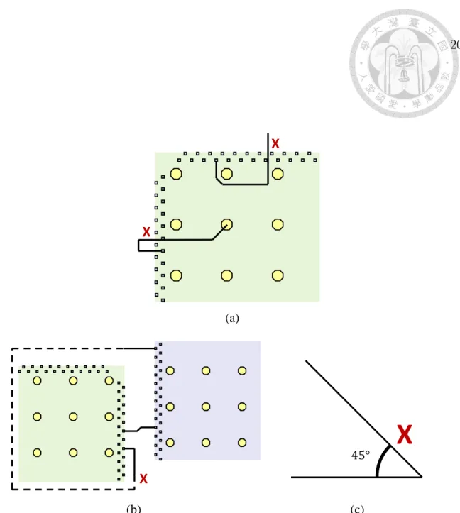
• Routing-region constraint: Because the distribution of I/O pads on chip bound- aries is very dense, detours/multiple crossings of a net on the chip boundaries are not allowed. As shown in Figure 2.2(a), the routed nets have some routed net segments in both the fan-in region (the region occupied by I/O pads is excluded) and the fan-out region, implying that some chip boundaries are crossed multiple times. In this work, we confine the routed nets with the routing-region constraint to avoid this undesired configuration.
• Non-detour-around-boundary constraint: A net is not allowed to make a long detour around the chip; for example, we set the upper bound of 25% of the chip perimeter in our implementation. If a single net detours around a chip, significant routing resources might be occupied, and routing failures might occur eventually. As shown in Figure 2.2(b), the net that detours around the chip would occupy significant routing resources; besides, the signal skew problem might occur due to the resulting long route. As a result, for any two chips, there must exist continuous intervals on the chip boundaries without pre-assignment I/O pads connecting each other, or there is no routing solution which satisfies this constraint.
(a)
(b)
X
X
X
(c)
45°
X
Figure 2.2: Three types of violations of the RDL layout constraints. (a) Violation of the routing-region constraint: both routed nets have some routed net segments in both the fan-in region (the region occupied by I/O pads is excluded) and the fan-out region. (b) Violation of the non-detour-around-boundary constraint: the routed net detouring around a large portion of the chip boundaries is not allowed. (c) Violation of the routing-angle constraint: the angle between two routing segments should be 90◦ or 135◦.
• Routing-angle constraint: A route can make a 90-degree (horizontally or ver- tically) or a 135-degree turn. However, a 45-degree turn is not allowed, as shown in Figure 2.2(c).
• Non-crossing constraint: Two nets cannot route across each other. To main- tain better signal integrity, vias are often not allowed for RDL routing. As a result, I/O pads and bump pads are punched through all RDLs, and each route is completed on a single layer [5]. Thus, net crossings are not allowed.
An RDL Routing Algorithm
In this chapter, we would first give an overview of our algorithm, and then detail the methods used in each stage of the algorithm.
3.1 Algorithm Overview
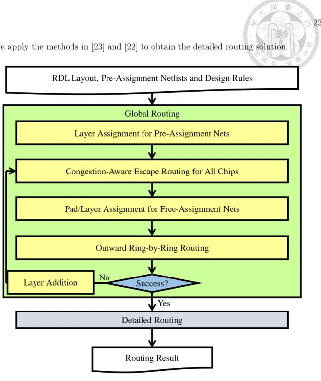
As shown in Figure 3.1, our global routing algorithm consists of four stages:
(1) layer assignment for pre-assignment nets, (2) congestion-aware escape routing for all chips, (3) pad/layer assignment for free-assignment nets, and (4) outward ring-by-ring routing.
In the first stage, we derive a concentric-circle model to represent the relative geometrical information of pre-assignment nets between one chip and all other chips, and then propose an efficient method to handle a layer-assignment problem for pre- assignment nets based on the derived model. With the layer-assignment information and congestion information, the second stage generates a routing prototype for fan- in bump pads by escape routing. The third stage constructs a flow network to assign free-assignment I/O pads to fan-out bump pads and escaped routes obtained in the second stage, and modifies the flow network with the concentric-circle model to consider pre-assignment nets. Finally, the fourth stage applies an outward ring- by-ring technique to route the nets in the fan-out region. After the global routing,
we apply the methods in [23] and [22] to obtain the detailed routing solution.
Global Routing
Layer Assignment for Pre-Assignment Nets
Congestion-Aware Escape Routing for All Chips RDL Layout, Pre-Assignment Netlists and Design Rules
Routing Result Detailed Routing
Pad/Layer Assignment for Free-Assignment Nets
Outward Ring-by-Ring Routing
Success?
Yes Layer Addition No
Figure 3.1: Overview of our proposed routing algorithm.
3.2 Layer Assignment for Pre-Assignment Nets
We start this section with a brief example. Given two pre-assignment nets as shown in Figure 2.2(b), if these two nets are routed on the same layer, a long detour
will occur, which violates the non-detour-around-boundary constraint mentioned in Section 2.2. As a result, it is desired to avoid the aforementioned situation by assigning pre-assignment nets to appropriate layers.
To achieve a layer assignment with good quality, we propose a concentric- circle model and a method to handle the layer-assignment problem for all pre- assignment nets. Our method simultaneously assigns a number of pre-assignment nets for one chip and proceeds to the other chips on the same layer. We proceed to a new layer if there are pre-assignment nets yet to be assigned.
3.2.1 Concentric-Circle Model
Our concentric-circle model consists of two concentric circles. The inner circle represents the chip ci, and the region outside the inner circle models the neighboring information of ci. Besides the two circles, there are nodes and bonds in this model.
We have the following definitions of a node and a bond.
Definition 1 A node in the concentric-circle model contains two types of informa- tion: a degree and its associated circle. The degree of a node in this model is the angle from the positive x-axis to the segment formed by the center of circles and the node. If a node is on the inner (outer) circle, we refer it as an inner (outer) node.
Definition 2 A bond starts from an inner node to an outer one. We define a bond by two degrees and a direction to describe how the bond traverses from the inner node to the outer node. The two degrees of a bond are defined by the degrees of its inner and outer nodes. The direction of a bond is either clockwise or counter-clockwise.
(a)
(b) (c)
: pre-assignment net : I/O pad order
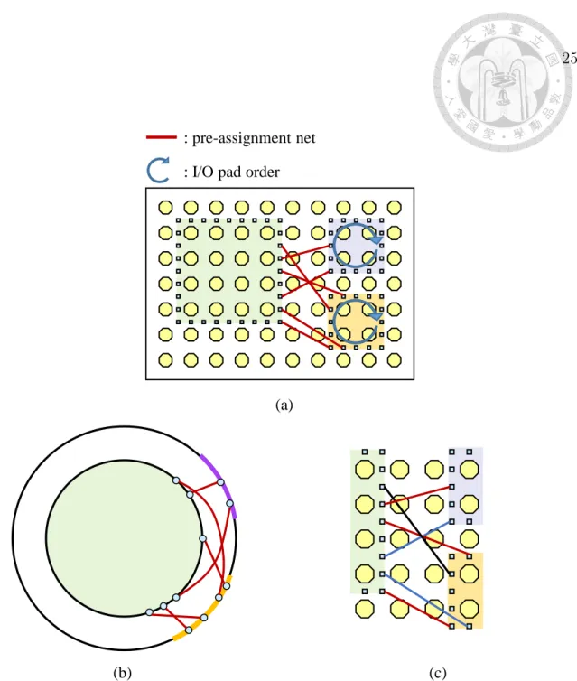
Figure 3.2: (a) An RDL layout with three chips and multiple pre-assignment nets.
The blue arcs indicate the orders of corresponding nodes of I/O pads that appear on our concentric-circle model. (b) The corresponding concentric-circle model of (a).
The inner circle represents the leftmost chip in (a), and the outer circle represents the neighboring geometry of the leftmost chip. The red arcs correspond to the pre- assignment nets connecting the nodes which represent the pre-assignment I/O pads.
(c) A sample solution of the layer-assignment problem. The nets of the same color are assigned to the same layer.
3.2.2 Construction of the Model for Layer Assignment for Pre-Assignment Nets
Each pre-assignment net belonging to the chip ci can be modeled with a bond in the concentric-circle model. The inner node of the bond represents the I/O pad belonging to ci. The outer node of the bond represents the other I/O pad. The degree of the inner node is determined by the angle from the positive x-axis to the segment formed by the center of ci and the corresponding I/O pad. To determine the degree of the outer node, we first introduce the definition of a degree interval.
Definition 3 A degree interval is a continuous range of degrees. The degree interval of a bond is the range starting from its inner node to its outer one.
Each chip to which ci connects can be modeled with a degree interval on the outer circle. For example, the two right chips in Figure 3.2(a) are mapped to the non-overlapping degree intervals in Figure 3.2(b) on the outer circle. The center of the degree interval of a chip is decided by the angle from the positive x-axis to the segment formed by the centers of ci and the chip. The related pre-assignment I/O pads of each chip are mapped to the chip’s degree interval starting from the I/O pad which is closest to the continuous interval on boundaries without pre-assignment I/O pads connecting to ci (as mentioned in Section 2.2) clockwise. Given an inner node and an outer node, there are two possible bonds of opposite directions. We choose the bond with a smaller degree interval to represent the pre-assignment net to avoid traversing a large portion of the inner circle.
3.2.3 Algorithm Based on the Model
We observe that if two bonds intersect, assigning the corresponding pre- assignment nets to the same layer would cause an inevitable detour. As a result, it is desirable to find a maximum set of non-intersecting bonds and assign the set of nets to the same layer to minimize the layer number. As shown in Figure 3.2, we first map the pre-assignment nets in Figure 3.2(a) to Figure 3.2(b) and perform the layer-assignment algorithm to obtain a sample solution as shown in Figure 3.2(c).
In the following, we detail the method of finding a set of non-intersecting bonds.
To explain our method, we first define a cutting bond.
Definition 4 A cutting bond is a bond that does not intersect any bond on the concentric-circle model.
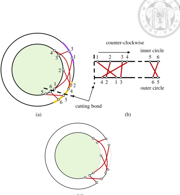
As shown in Figure 3.3(a), if there is a cutting bond, we reduce the problem into an LCS problem by transforming the cyclic structure of the model into a se- quential structure, as shown in Figure 3.3(b). The nodes on the upper (lower) line follow the same order as on the inner (outer) circle, starting from the cutting bond counter-clockwise. If there are reversed numbers between the sequences of upper and inner lines, some bonds intersect. We apply the LCS algorithm in [25] on the two sequences to obtain a maximum set of non-intersecting bonds.
In order to find a cutting bond, we determine whether two bonds intersect in terms of degrees. If the directions of two bonds are the same, two bonds intersect if and only if the degree interval of one bond completely lies within the other one.
If the directions of two bonds are different, two bonds intersect if and only if the degree intervals of the two bonds share some degrees. If any two bonds intersect,
(a) (b)
(c)
cutting bond
counter-clockwise
outer circle inner circle 4
2 3 5
1 6
1 2
4 3 6 5
1
1 2
2 3
4 3
5 4
6 5 6
Figure 3.3: An example of our concentric-circle model in layer assignment for pre- assignment nets. (a) The same concentric-circle model as Figure 3.2 with a cutting bond. (b) The LCS problem converted from (a). The upper (lower) line corresponds to the inner (outer) circle in (a), and the nodes on the upper (lower) line follow the same order as on the inner (outer) circle, starting from the cutting bond counter- clockwise. (c) Candidate locations for a cutting bond on an inner (outer) circle denoted in solid black arcs. If any two bonds intersect, some degree intervals on the two circles are excluded from consideration because no cutting bond will co-exist with an intersection.
some degree intervals on the two circles are excluded from consideration because no cutting bond will co-exist with an intersection. As shown in Figure 3.3(c), the solid arcs in the inner (outer) circle are candidate degrees for a cutting bond on the inner (outer) circle. Therefore, we construct two interval trees to find all the intersections between all the bonds and identify the excluded degree intervals on the two circles. One of the interval trees represents the degree intervals of the clockwise bonds, and the other represents the degree intervals of counter-clockwise bonds.
Then, we obtain candidate degree intervals on the two circles. We choose a degree on any inner candidate degree interval and form bonds with all outer candidates.
Then, we use the interval trees to find a cutting bond. If there is no cutting bond, we find a bond intersecting the minimized number of the bonds on the concentric- circle model, remove these bonds and convert the problem into an LCS problem.
The candidate inner (outer) degrees of the bond are any degree of degree intervals between any two adjacent nodes on the inner (outer) circle. Again, we use the two interval trees to find the bond intersecting the minimized number of the bonds on the model.
If some of the pre-assignment nets of the chip ci have been assigned to the same layer, the original problem is decomposed into multiple LCS problems due to the corresponding bonds. Besides, if some previously assigned pre-assignment nets which do not connect to ci, the concentric-circle model needs to be updated by trimming nodes on the corresponding degree intervals on the outer circle.
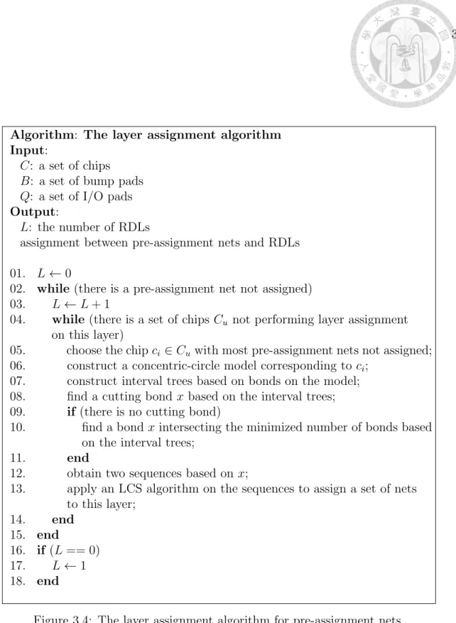
Figure 3.4 summarizes our proposed layer assignment method. Line 1 sets the initial number of RDLs to zero. Lines 2–15 perform layer assignment if there is still a pre-assignment net not assigned. Lines 4–14 perform layer assignment for pre-assignment nets belonging to a single chip based on our concentric-circle model.
Lines 16–18 set the number of RDLs to one if there is no pre-assignment net.
Algorithm: The layer assignment algorithm Input:
C: a set of chips B: a set of bump pads Q: a set of I/O pads Output:
L: the number of RDLs
assignment between pre-assignment nets and RDLs 01. L ← 0
02. while (there is a pre-assignment net not assigned) 03. L ← L + 1
04. while (there is a set of chips Cu not performing layer assignment on this layer)
05. choose the chip ci ∈ Cu with most pre-assignment nets not assigned;
06. construct a concentric-circle model corresponding to ci; 07. construct interval trees based on bonds on the model;
08. find a cutting bond x based on the interval trees;
09. if (there is no cutting bond)
10. find a bond x intersecting the minimized number of bonds based on the interval trees;
11. end
12. obtain two sequences based on x;
13. apply an LCS algorithm on the sequences to assign a set of nets to this layer;
14. end
15. end
16. if (L == 0) 17. L ← 1 18. end
Figure 3.4: The layer assignment algorithm for pre-assignment nets.
We have the following theorem for the time complexity of the method.
Theorem 1 If there is a cutting bond, our method finds a maximum set of non- intersecting bonds in O(milg mi + I1 + I2) time; otherwise, the method obtains a maximized set of non-intersecting bonds in O(m2i lg mi + I3) time, where mi is the number of the pre-assignment nets of the chip ci, I1 is the number of the intersections between bonds of pre-assignment nets, I2 is the number of the intersections discovered in the checking process for finding a cutting bond, and I3 is the number of the intersections discovered in the process for finding a bond intersecting the minimized number of the bonds.
Proof 1 We can obtain the concentric-circle model in O(mi) time, where mi is the number of the pre-assignment nets of the chip ci. The two interval trees can be obtained in O(milg mi)) time. The time complexity of querying all the intersections between all the bonds is O(milg mi + I1). Because the number of candidate degree intervals on the outer circle is O(mi), we can obtain a cutting bond (if it exists) in O(milg mi + I2) time. Finally, we apply the LCS algorithm proposed in [25] whose time complexity is O(milg mi). Note that the numbers on the upper (lower) line are all different, the time complexity is thus reduced from O(m2i) to O(milg mi). If there is no cutting bond, we try O(m2i) choices of bonds to find out the bond intersecting the minimized number of the bonds on the model in O(m2i lg mi+ I3) time.
3.3 Congestion-Aware Escape Routing for All Chips
After finishing the layer assignment for pre-assignment nets, we perform es- cape routing for all chips considering congestion information to finish the routing in the fan-in region. The escape routing problem has been extensively studied in recent years, which is to route specified bump pads in a bump pad array to the
boundaries of the array [29]. In our problem, a bump pad can be connected to any I/O pad, so we do not need to consider the ordering constraints in [21].
: vertex capacity = 𝐷−𝑐𝑎𝑝 − 2 ∙ 𝑂−𝑐𝑎𝑝/2
: diagonal cut : orthogonal cut : capacity = 𝑂−𝑐𝑎𝑝 : capacity = 1 : capacity = ∞
: capacity = 𝑂−𝑐𝑎𝑝/2 N
E
S
W C
Figure 3.5: The network flow model inside a tile with four bump pads proposed by [29].
Because multiple chips share the same RDLs, we have to consider the routing resource allocation in the fan-out region during escape routing. Based on the tile model proposed in [29], we further make some modifications to perform escape routing while minimizing potential routing congestion. Here, we make a brief review on the tile model. A tile consists of four adjacent bump pads, as shown in Figure 3.5.
O-cap denotes the maximum number of nets which can pass through one side of the tile simultaneously, and D-cap is the maximum number of nets which can pass through the diagonal of the tile simultaneously. There are two super vertices, the source vertex and the sink vertex. There are directed edges from the source vertex to the bump pads which need to escape to the array boundaries. All edges, the red arrows in Figure 3.6, from the boundary tiles to the outside of the array are connected to the sink vertex of a flow network. The inter-tile edges are assigned unit costs, while all the other edges are assigned zero costs. To handle multiple layers, we duplicate some vertices and edges for each layer without duplicating the vertices for
bump pads (similar to the technique in [5]). After the flow network construction, we apply the minimum-cost maximum-flow (MCMF) algorithm [1] to obtain escaped routes while minimizing the total wirelength.
boundary capacities
pre-assignment I/O pads
Figure 3.6: An example of the flow network of one chip. By adjusting the boundary capacities of the flow network according to (1) the resulting cost of a bipartite matching and (2) the locations of pre-assignment I/O pads, we can achieve a good distribution of nets after escape routing considering the congestion of the whole layout.
We adjust the capacities of the edges connected to the sink vertex (the red arrows in Figure 3.6) to control every maximum number of routes passing through all intervals of the array boundaries. To decide the value of its capacity, we calculate the cost (not the cost in the flow network) for each edge connecting to the sink vertex. The cost contains the bipartite cost CB and the pre-assignment cost CP.
cost = αCB+ βCP, (3.1)
where α and β are user-defined parameters. CP is equal to the number of neighboring pre-assignment I/O pads on the same layer. For CB, we construct a bipartite graph GB = (VB, EB), where VBis a set of vertices corresponding to all the free-assignment I/O pads and bump pads, and EB is a set of edges. For a free-assignment I/O pad and a fan-out bump pad, we construct an edge between their corresponding vertices. For a free-assignment I/O pad qji and a fan-in bump bik (both pads belong to the chip ci), we construct an edge between their corresponding vertices. Each edge has an associated weight which equals the Euclidian distance between the corresponding pads. Then, we perform the minimum-weight maximum-cardinality bipartite matching algorithm [13]. For each edge connecting to the sink vertex, the corresponding bipartite cost is the sum of the matched edge weights of the neighboring free-assignment I/O pads. The capacity of an edge connecting to the sink vertex is proportional to the cost and less than O-cap.
We have the following theorem for the time complexity of the method.
Theorem 2 The overall time complexity of this method is O((|B|+|Q|)3+L2P
j|Bij|3), where B is the set of all the bump pads, Q is the set of all the I/O pads, L is the current number of layers, and Bij is the set of the bump pads belonging to the chip cj.
Proof 2 The time complexity of the minimum-weight maximum-cardinality bipar- tite matching algorithm is O((|B| + |Q|)3) because the number of vertices in GB is O(|B| + |Q|). The time complexity of the MCMF algorithm for a chip cj is O(L2|Bij|3) because the maximum flow of the network for cj is O(|Bij|), and the number of vertices is O(L |Bij|).
3.4 Pad/Layer Assignment for Free-Assignment Nets
After the escape routing stage, we construct a flow network and apply the minimum-cost maximum-flow (MCMF) algorithm [1] to assign all free-assignment I/O pads to the fan-in region (the escaped routes and the outermost bump pads of bump pad arrays inside the chips) and the fan-out region (the fan-out bump pads). We refer to the outermost bump pads of bump pad arrays inside the chips as boundary bump pads. Note that at this stage, we have layout information of the finished routes in the fan-in region and the layer-assignment results of pre- assignment nets (actual routes are yet to be determined). To fully integrate all the layout information into our flow network model, we remove some edges while considering the pre-assignment nets.
First, we introduce the construction of the flow network. Then, we modify the flow network considering the pre-assignment nets. Every free-assignment I/O pad and every escaped route correspond to a vertex in the flow network. For each fan-out and boundary bump pad, L duplicated vertices are created to represent the same-location bump pad on each layer, where L is the current number of layers.
To ensure that each fan-out and boundary bump pad is assigned only on one layer, another vertex as a super vertex is created for each fan-out and boundary bump pad.
In addition, two super vertices, which are the source vertex and the sink vertex, are created in the flow network. There are six types of directed edges:
• Edges from the vertex for a free-assignment I/O pad to the L duplicated vertices for a fan-out bump pad or a neighboring boundary bump pad.
• Edge from the vertex for a free-assignment I/O pad to the vertex for a neigh- boring escaped route.
• Edges from the L duplicated vertices for a fan-out bump pad or boundary bump pad to the super vertex for the same bump pad.
• Edge from the source vertex to the vertex for a free-assignment I/O pad.
• Edge from the super vertex for a fan-out bump pad or boundary bump pad to the sink vertex.
• Edge from the vertex for an escaped route to the sink vertex.
Every edge has a unit capacity. The edge cost of the first type is the Euclidian distance between the two pads. The edge cost of the second type is the wirelength of the escaped route plus the Euclidian distance between the I/O pad and the bump pad array boundary location of the escaped route. All the other edges have zero costs.
To consider the pre-assignment nets, we need to remove some edges in the flow network to avoid potential detours or routing failures. As shown in Figure 3.7(a), assigning the I/O pad q11 to the bump pad bo3 would lead to an inevitable detour, due to the bottom pre-assignment net. We use the concentric-circle model to identify edges which might lead to detours and remove them. For each chip on each layer, we first construct a concentric-circle model with bonds of the pre-assignment nets of the chip on the layer. Taking Figures 3.7(a) and (b) as an example, the gray regions are to-be-checked regions (degree intervals) in which, if other nets exist, some detours might occur. Note that the method to decide the degree of an outer node is different from the one in Section 3.2. To map a pre-assignment or a free-assignment net to a bond, the degree of its outer node is decided by the angle from the positive x-axis to the segment formed by the center of the chip to the I/O pad or the bump pad.
After the construction of the concentric-circle model for each chip on each layer,
(a) (b) : pre-assignment net
: to-be-checked region/degree interval
: no-check-needed net : check-needed net
𝑞𝑞11 𝑏𝑏1𝑜𝑜
𝑏𝑏3𝑜𝑜 𝑏𝑏2𝑜𝑜
𝑏𝑏2𝑜𝑜 𝑏𝑏3𝑜𝑜 𝑞𝑞11
𝑏𝑏1𝑜𝑜
Figure 3.7: An example of our concentric-circle model in the stage of pad/layer assignment for free-assignment nets. (a) A sample layout with two pre-assignment nets. q11 is the I/O pad of consideration, and bo1, bo2, and bo3 are the candidate bump pads to be connected to. The to-be-checked regions are constructed from the perspective of the leftmost chip based on the pre-assignment nets connecting to it.
(b) The corresponding concentric-circle model of (a). The inner circle represents the leftmost chip in (a). The red and blue arcs are the degree intervals derived from the layout. Starting from q11, the red ones are the ones that need to be checked whether a potential detour may occur because they overlap with the bottom to-be-checked region, whereas the blue one needs not be checked.
all the to-be-checked degree intervals are formed based on the pre-assignment nets.
We then construct an interval tree to store all the to-be-checked degree intervals for each chip on each layer. We use interval trees to decide whether edges of the overall flow network may need to be removed to avoid potential detours. Finally, we check the results obtained by the interval trees to actually remove them by the physical locations of the pads. As shown in Figure 3.7(b), the edge from q11 to bo2 and the edge from q11 to bo3 may need to be removed (we exclude the edge from q11 to bo1 based on the interval tree). According to Figure 3.7(a), the edge from q11 to bo3 should actually be removed.
𝑞𝑞𝑏𝑏𝑘𝑘 𝑞𝑞𝑎𝑎𝑗𝑗
𝑏𝑏𝑒𝑒𝑜𝑜
𝑏𝑏𝑓𝑓𝑜𝑜
Figure 3.8: Assume there is a crossing consisting of edges (the solid lines) at the layer l1 in an MCMF result, and there are an edge between qja and boe at the layer l2 and an edge between qbj and bof at the layer l3. This contradicts the fact that the total cost of the MCMF result is minimum.
Because we use the Euclidian distance as the cost metric (see Figure 3.8) and consider the pre-assignment nets, very few crossings will be introduced. In addition, we can distribute I/O pads to all the layers evenly by adjusting the edge costs. There is an additional cost on the edges from an I/O pad to the vertices on some layers. Because there is a minimum distance between an I/O pad and a bump pad, we can choose the additional cost small enough which would not violate the property in Figure 3.8. Hence, the result of the MCMF algorithm is a good
assignment topology which facilitates the following stages.
We have the following theorem for the time complexity of the method.
Theorem 3 The overall time complexity of this method is O(|Q| (L |B| + |Q|)2), where Q is the set of all the I/O pads, L is the current number of layers, and B is the set of all the bump pads.
Proof 3 We can construct the original flow network in O(|B| |Q|) time. The time complexity of removing undesired edges is O(|B| |Q| lg |N |+I4), where I4 = O(|B| |Q| |N |) is the number of intersections between the degree intervals of bonds of free-assignment nets and pre-assignment nets. The time complexity of the MCMF algorithm is O(|Q| (L |B|+|Q|)2) because the maximum flow is O(|Q|) and the number of vertices is O(L |B| + |Q|). Hence, the time complexity of the method is dominated by the MCMF algorithm.
3.5 Outward Ring-by-Ring Routing
Based on the MCMF result, all connections of I/O pads are determined. In this stage, we will finish the routing topology for each net in the fan-out region, based on a ring-by-ring, chip-by-chip scheme. Starting from the I/O pads, for each ring formed by the bump pads, we will assign correct ring passing points for all I/O connections in the fan-out region. To correctly assign the ring passing points, we have to fix two types of violations between two adjacent rings: (1) the net order violation and (2) the tile capacity violation. Because net crossings are not allowed, the net order on any two adjacent rings should match. Besides, we have to check if a given set of currently assigned net segments can pass through a tile simultaneously.
First, we can fix net order violations by either reassigning some I/O pads to bump pads, detouring the pre-assignment net, or reassigning some I/O pads to
escaped routes or boundary bump pads in the fan-in region, as shown in Figure 3.9.
Pre-assignment nets break two adjacent rings into many segments. The net orders of two corresponding segments on the inner and outer rings should be the same. If all order violations are free-assignment nets, we can reassign them to correct the order. If a net order violation involved a pre-assignment net, we have to detour the pre-assignment net or reassign free-assignment I/O pads to the fan-in region with unassigned escaped routes or boundary bump pads.
After correcting all net order violations, we check capacities of tiles by the tile routability analyzer proposed in [18]. The analyzer can check if a given set of currently assigned net segments can pass through a tile simultaneously in constant time. If a tile capacity violation occurs, we cluster the tile with an adjacent tile to push some net segments into the adjacent tile, as shown in Figure 3.9. It may need to cluster more adjacent tiles to fix a tile capacity violation. We can also reassign some I/O pads to escaped routes or boundary bump pads in the fan-in region.
(a) (b)
…
…
……
1𝑠𝑠𝑠𝑠 2𝑛𝑛𝑛𝑛
… …
……
1𝑠𝑠𝑠𝑠 2𝑛𝑛𝑛𝑛
3𝑟𝑟𝑛𝑛 : net order violation
: tile capacity violation : bump pad ring
: pre-assignment net : free-assignment net : ring passing point
Figure 3.9: An example for our outward ring-by-ring routing algorithm. (a) The global routing result with two types of violations after finishing the first ring. All the I/O pads are assigned to correct ring passing points on the first ring. The ring passing points on the first ring are connected to the targets. (b) The global routing result after finishing the second ring. All the violations in (a) are corrected by reassigning some I/O pads to bump pads or detouring the pre-assignment net.
![Figure 1.1: (a) The cross view of a traditional flip-chip package [15]. (b) The cross view of a multi-chip InFO WLCSP.](https://thumb-ap.123doks.com/thumbv2/9libinfo/9599186.628603/17.892.287.707.154.847/figure-cross-traditional-package-cross-multi-info-wlcsp.webp)
![Figure 1.3: Classification of RDL routing problems for traditional flip-chip packages according to the RDL structures and assignment types between I/O pads and bump pads [15].](https://thumb-ap.123doks.com/thumbv2/9libinfo/9599186.628603/20.892.167.729.336.755/figure-classification-problems-traditional-packages-according-structures-assignment.webp)
![Figure 1.4: An example flow network construction [8, 9]. (a) Construction of tile and intermediate nodes](https://thumb-ap.123doks.com/thumbv2/9libinfo/9599186.628603/22.892.157.735.321.740/figure-example-flow-network-construction-construction-intermediate-nodes.webp)
![Figure 1.5: Comparisons of the previous work [10] with extensions and our algo- algo-rithm](https://thumb-ap.123doks.com/thumbv2/9libinfo/9599186.628603/28.892.109.803.106.861/figure-comparisons-previous-work-extensions-algo-algo-rithm.webp)