行政院國家科學委員會專題研究計畫 成果報告
高性能溝渠式閘極功率金氧半場效電晶體之研製
計畫類別: 個別型計畫
計畫編號: NSC92-2215-E-011-004-
執行期間: 92 年 08 月 01 日至 93 年 07 月 31 日 執行單位: 國立臺灣科技大學電子工程系
計畫主持人: 莊敏宏
計畫參與人員: 黎志建 邱義銘 鄭士豪 楊智翔
報告類型: 精簡報告
處理方式: 本計畫可公開查詢
中 華 民 國 93 年 9 月 21 日
中文摘要
本計劃在雙重擴散式電晶體及溝渠式閘極功率電晶體兩種結構的 n 型磊晶區域中,加
入p-column 區域來改善傳統功率電晶體的元件特性,設計係針對耐壓為 30 V 的操作。
對DMOSFET with p-column 的結構而言,當元件大小為 5 µm 時,其可得一 0.087 mΩ-cm2
之特性電阻,而在加入p-column 後,就可以得到一個 0.068 mΩ-cm2的低電阻值。元件是
利用電晶體中電荷補償的觀念。因此跨在外加的p-column 及 n 型磊晶接面上的最大電場
將會減小,如此一來,元件的耐壓就可以提升。藉由提高 n 型磊晶區域的濃度,將會得
到一個低電阻值而可以有效降低元件的導通電阻將近 22 %。另一方面,對 Trench-gate
power MOSFET with p-column 結構而言,p-column 的横向撗散使導通區域變窄,導通電
阻值增大;考慮在元件大小為2 µm,所獲得的特徵導通電阻值是 0.078 mΩ-cm2,這個值
比傳統溝渠式閘極功率電晶體的電阻還大。最後,發現當p-column 與閘極區域間的距離
大於約0.65 微米時,可得到比傳統結構更低的導通電阻。
英文摘要
In this project, two device structures, the DMOSFET and the trench-gate power MOSFET, with p-columns in the n-epitaxial region are analyzed. The effects of the p-column implantation on the blocking ability and the on-state resistance are studied. For the DMOSFET with p-column structure, a traditional DMOSFET with the cell pitch size of about 5 µm can cause a specific on-state resistance of about 0.087 mΩ-cm2 with a blocking voltage of 30 V. A significantly better specific on-state resistance of 0.068 mΩ-cm2 can be obtained by using p-columns. The device is based on the charge compensation effect in the n-epitaxial region of the transistor. The maximum electric field developed at the p-base/n-drift junction is reduced allowing higher breakdown voltage. By using the epitaxial layer with higher doping concentration, a low specific on-state resistance can be obtained. The usage of p-columns further reduces the specific on-state resistance to be approximately 22 % lower. In terms of trench-gate power MOSFET with p-column structure, however, additional lateral diffusion would largely increase on-state resistance by narrowing the conduction region. Therefore, considering a cell pitch size of 2 µm, the specific on-resistance is about 0.078 mΩ-cm2 larger than that for the traditional trench-gate power MOSFET. It is however found that when the distance between the p-column and the gate region larger than about 0.65µm, the usage of p-column can further improve the trench-gate power MOSFET.
1. 前言及研究目的
In the last twenty years, since power semiconductor technology has continually been developed, performances of power electronic systems, such as scaling of applied voltage, power dissipation, switching speed, etc, have been greatly promoted [1-13]. Many different types of power MOSFET structure have been proposed and a continuous progress toward obtaining a lower on-resistance has been made too. In order to reduce the power dissipation, some ideas on semiconductor devices have been proposed to overcome the limit of the ideal specific on-resistance.
In this project, based on charge compensation effect, p-column structure is formed within the n-epitaxial region for the DMOS and the trench-gate power MOSFET. As an example, a trench-gate power MOSFET with p-column structure is schematically shown in Fig. 1. By increasing the doping concentration of the n- drift region, and further counterbalancing this additional charge by the implementation of p-column structure, a lower specific on-state resistance can be obtained with the blocking voltage being retained.
2. 研究方法
The self-aligned silicide (salicide) process is used to form a silicided trench-gate power MOSFET with p-column structure. The Sb-doped wafers of 1×1019 cm-3 with n-epitaxial layer of 2.5 µm and 2×1016 cm-3 are used. The process steps include (1) Field oxidation of 5000 Å at 1050 °C. (2) Mask 1, defining active area. (3) Screen oxide of 15 nm thickness grown at 950
°C. (4) Mask 2, defining P-column area. (5) P-column implantation of B+(800 keV, 3×1013 cm-2). (6) Dopant drive-in at 1050 °C for 120 min and removal of field oxide. (7) Screen oxidation of 15 nm thickness grown at 950 °C. (8) P-base implantation of B+(60 keV, 1×1013 cm-2). (9) Dopant drive-in at 1050 °C for 120 min and removal of field oxide. (10) LPCVD oxide of 600 nm thickness as hard mask. (11) Mask 3, defining the trench region. (12) Trench Si etching of about 1 um thickness. (13) Sacrificial oxidation of about 15 nm thickness in an N2O ambient. (14) Removal of sacrificial oxide and gate oxidation of 50 nm thickness at 950
°C. (15) LPCVD poly-Si gate and POCl3 diffusion at 950 °C. (16) Poly-Si etching back, to form poly-Si plug as the trench gate. (17) Removal of hard-mask oxide. (18) Source implantation of As+ (30 keV, 1×1014 cm-2). (19) LPCVD oxide of about 200 nm thickness, and then etching to form oxide spacer. (20) Co-salicide process, forming silicide at source and gate regions. (21) Mask 4, defining contact hole. (22) Al sputtering of about 4 um thickness. (23) Mask 5, defining metal pad. On the other hand, the fabrication process for DMOS with p-column is similar to the above procedure.
As for the above process, we optimize the device characteristics by changing some process and device parameters. These parameters include the p-column implantation dose, the p-column implantation energy, the p-column mask width, the p-column implantation, the drive-in temperature and drive-in time, the concentration of epitaxial layer. The blocking voltage is conducted at the gate voltage of 0 volt, and the on-state resistance is obtained at the gate bias of 15 volt.
3. 結果與討論
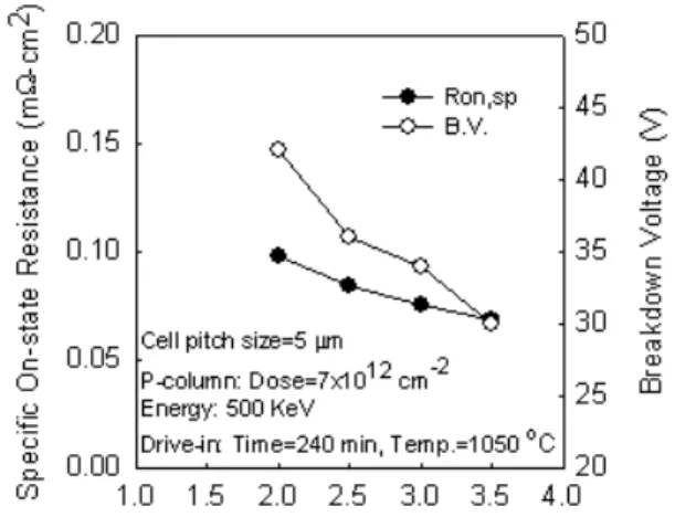
In the DMOSFET with p-column, the p-column structure will affect the conducting current by extending into the n-epitaxial region. Hence, the p-column implantation dose must be suitable. Too heavy or too light p-column implantation dose will cause a relatively low breakdown voltage. Furthermore, higher implantation energy can lead to a higher breakdown voltage, but easily cause the formation of floating region. Figure 2 shows the dependence of specific on-state resistance and blocking voltage on p-column implantation dose for power DMOSFET with p-column structure. And in order to save cost, relatively low drive-in temperature and time should be expected, and thus the drive-in condition of 1050 °C and 240 min can be the suitable condition here. In addition, by using the epitaxial layer with higher concentration, smaller specific on-state resistance can be achieved, but worse blocking ability and p-column floating may be caused. Figure 3 shows the dependence of specific on-state resistance and blocking voltage on doping concentration of n- drift region for DMOSFET with p-column structure.
Therefore, the appropriate p-column doping profile, drive-in condition, and dopant concentration of epitaxial layer should be chosen. For the operation at a gate bias of 15 V, the optimal process conditions are with the p-column implantation dose and energy of 8×1012 cm-2 and 400 keV, drive-in temperature and time of 1050 °C and 240 min, and epitaxial layer of dopant concentration of 4×1016 cm-3. A power DMOSFET with a blocking voltage of 30 V and a specific on-state resistance as low as 0.068 mΩ-cm2 can be achieved.
In the p-column trench-gate power MOSFET structure, it is found that the p-column region largely affects the on-state conduction, attributable to the small distance between the p-column
and gate region. Subtle changes in implantation conditions would affect the specific on-state resistance considerably. The p-column region with too heavy or too light doping concentration will cause relatively low breakdown voltage. As a result, the optimal process conditions are with p-column implantation dose and energy of 1.6×1013 cm-2 and 300 keV, no drive-in thermal cycle, mask width of 0.1 µm and the epitaxial layer of dopant concentration of 5×1016 cm-3. Accordingly, the blocking ability can be qualified at 30 V and the specific on-state resistance will be estimated to be 0.074 mΩ-cm2 at a gate bias of 15 V. Nevertheless, when cell pitch size is 2 µm, the specific on-state resistance of p-column trench-gate power MOSFET is higher than the traditional trench-gate power MOSFET. Figure 4 shows the dependence of specific on-state resistance and blocking voltage on p-column implantation dose for trench-gate power MOSFET with p-column structure.
By examining the cell pitch size of 3, 4 and 5 µm, it is found that the distance between the p-column region and the trench-gate region must be larger than about 0.65 µm. When the cell pitch size is 2 µm, the distance between the p-column region and the gate region cannot be large enough to derive better specific on-state resistance by using the p-column structure. With larger p-column mask width, the specific on-state resistance will be increased. However, with smaller column mask width, the breakdown voltage will be improved slightly. Therefore, there is a trade-off for the p-column mask width. For a cell pitch size of 3 µm, the optimal conditions are with p-column implantation dose and energy of 8×1012 cm-2 and 500 keV, no drive-in thermal cycle, and the epitaxial layer of dopant concentration of 5×1016 cm-3. A specific on-state resistance of 0.125 mΩ-cm2 can be obtained.
4. 結論
In this project, two device structures, the DMOSFET and the trench-gate power MOSFET, with p-columns in the n-epitaxial region are analyzed. The effects of the p-column implantation on the blocking ability and the on-state resistance are studied. For the DMOSFET with p-column structure, a traditional DMOSFET with the cell pitch size of about 5 µm can cause a specific on-state resistance of about 0.087 mΩ-cm2 with a blocking voltage of 30 V. A significantly better specific on-state resistance of 0.068 mΩ-cm2 can be obtained by using p-columns. The device is based on the charge compensation effect in the n-epitaxial region of the transistor. The maximum electric field developed at the p-base/n-drift junction is reduced allowing higher breakdown voltage. By using the epitaxial layer with higher doping concentration, a low specific on-state resistance can be obtained. The usage of p-columns further reduces the specific on-state resistance to be approximately 22 % lower. In terms of trench-gate power MOSFET with p-column structure, however, additional lateral diffusion would largely increase on-state resistance by narrowing the conduction region. Therefore, considering a cell pitch size of 2 µm, the specific on-resistance is about 0.078 mΩ-cm2 larger than that for the traditional trench-gate power MOSFET. It is however found that when the distance between the p-column and the gate region larger than about 0.65µm, the usage of p-column can further improve the trench-gate power MOSFET.
5. 參考文獻
[1] D. Ueda, H. Takagi, and G. Kono, IEEE Trans. Electron Dev. 1985;32:2.
[2] H.R. Chang, and B.J. Baliga, IEEE Trans. Electron Dev. 1989;36:1824.
[3] M. Kitagawa, I. Omura, S. Hasegawa, T. Inoue, and A. Nakagawa, IEDM Tech. 1993:679.
[4] M. Harada, T. Minato, H. Takahashi, H. Inoue, and I. Takata, Proceedings of 6th ISPSD 1994:411.
[5] F. Udrea, and G.A.J. Amaratunga, Proceedings of 7th ISPSD 1995:190.
[6] I. Omura, T. Ogura, K. Sugiyama, and H. Ohashi, Proceedings of 9th ISPSD 1997:217.
[7] T. Laska, P. Pfirsch, F. Hirler, I. Niedermeyr, C. Schaffer, and T. Schmidt, Proceedings of 10th ISPSD 1998:433.
[8] F. Udrea, P.R. Waind, J. Thomson, T. Trajkovic, S.S.M. Chan, S. Huang, and G.A.J.
Amaratunga, Proceedings of 11th ISPSD 1999:141.
[9] F. Udrea, and G.A.J. Amaratunga, IEEE Trans. Electron Dev. 1995;42:1356.
[10] T. Nitta, A. Uenishi, T. Minato, S. Kusunoki, T. Hashi, H. Nakamura, K. Nakamura, S.
Aono, and M. Harada, Proceedings of 10th ISPSD 1998:43.
[11] T. Trajkovic, F. Udrea, P.R. Waind, J. Thomson, G.A.J. Amaratunga, and W.I. Milne, IEE Proc.-Circuits Devices Syst. 2001;148:71.
[12] G. Deboy, H. Husken, H. Mitlehner, and R. Rupp, IEEE BCTM 8.1 2000:134.
[13] M.H. Juang, L.C. Sun, W.T. Chen, and C.I. Ou-Yang, Solid-State Electronics 2001;45:169.
6. 圖示及說明
Fig. 1 The resultant device structure for trench-gate power MOSFET with p-column region.
Fig. 2 Dependence of specific on-state resistance and blocking voltage on p-column implantation dose for power DMOSFET with p-column structure.
Fig. 3 Dependence of specific on-state resistance and blocking voltage on doping concentration of n- drift region for DMOSFET with p-column structure.
Fig. 4 Dependence of specific on-state resistance and blocking voltage on p-column implantation dose for trench-gate power MOSFET with p-column structure.
成果自評報告
本計劃在雙重擴散式電晶體及溝渠式閘極功率電晶體兩種結構的 n 型磊晶區域中,加入 p-column 區域來改善傳統功率電晶體的元件特性,設計係針對耐壓為 30 V 的操作。對 DMOSFET with p-column 的結構而言,可得到一個低電阻值而可以有效降低元件的導通 電阻將近22 %。另一方面,對 Trench-gate power MOSFET with p-column 結構而言,當 p-column 與閘極區域間的距離大於約 0.65 微米時,也可得到比傳統結構更低的導通電 阻。本計劃結果具高功率元件技術之研究價值,已準備投稿國際性學術期刊。
可供推廣之研發成果資料表
□ 可申請專利 □ 可技術移轉 日期: 年 月 日
國科會補助計畫
計畫名稱:
計畫主持人:
計畫編號: 學門領域:
技術/創作名稱
發明人/創作人
中文:
(100~500 字)
技術說明
英文:
可利用之產業 及 可開發之產品
技術特點
推廣及運用的價值 附件二