Abstract—The design and analysis of a compact flyback AC to DC power supply is described and simulation results are presented. Of particular interest is merging two interleaved power converters such that the main switch in one converter behaves as the clamp switch of the other while ripple cancellation is accomplished. Also, PFC and ZVZCS are achieved with no extra components. Using these approaches, the total number of active and passive components used and consequently the associated power loss, complexity and cost is reduced, which makes the design appealable for low-power high-volume applications. The proposed circuit converts 110VAC to 230VDC at 2.2A load current with an overall simulated efficiency of around 93%.
Keywords—Merged, interleaved, flyback, PFC, active clamp, ZVZCS.
I. I NTRODUCTION
To reduce the weight and size of a power converter, it is desired to use a high switching frequency while it has been reported that low frequency isolated converters have better efficiencies [1]. Lower efficiency at higher frequencies is mainly due to increased switching losses that can be compensated using zero voltage/current switching techniques [2].
In an effort to increase conversion efficiency, [3]
proposes an AC to DC converter based on flyback topology that recovers the surge energy generated by parasitic inductances to the output side of the isolation transformer. Additional circuitry is used to achieve zero voltage switching (ZVS) during turn on, and voltage clamping during turn off, of the main switch.
In this paper a merged interleaved flyback power factor corrected (PFC) converter with active clamp and zero-voltage zero-current switching (ZVZCS) is introduced. The single-stage conversion proposed here has high power factor, improved efficiency and simple structure with very low number of parts used, which reduces manufacturing cost. Because of these advantages, this converter is recommended for low-power high- volume applications.
Major features of this design are:
• Reduced the total number of components used by merging two parallel power converters and by utilizing single-stage PFC approach.
• Reduced the size of input and output filter components by increasing (constant) switching frequency and by interleaving phases.
• Increased power rating by paralleling phases (not paralleling switches).
• Increased converter output voltage by putting secondary side of the isolation transformers in series (lowered transformer turns ratio).
• Suppressed unwanted voltage surge and oscillations across switches using non-dissipative active clamping without using auxiliary circuitry.
• ZVZCS operation without using auxiliary circuitry.
• PFC functionality without using extra control and current sensing circuitry.
II. C IRCUIT D ESIGN
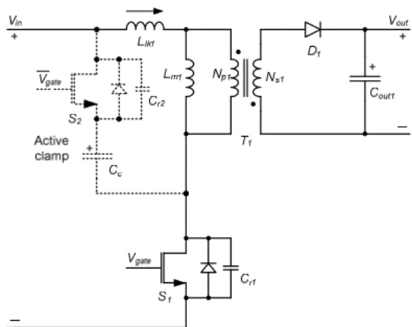
A. Flyback converters with active clamp and ZVZCS A conventional flyback converter is shown in Figure 1 using solid lines. It is an isolated topology that is derived from the non-isolated buck-boost configuration. When the main switch S
1is turned on, current builds up in the magnetizing inductance L
m1of the isolation transformer.
The transformer winding polarity is set so that a positive output voltage is obtained. Because of the transformer winding polarity, output diode D
1becomes reversed biased. As such, current does not flow simultaneously in both windings of a flyback transformer, as opposed to the forward topology where current flows simultaneously in both windings and need a demagnetizing winding. The transformer polarity convention used here is: if current flows into the dotted terminal of the primary winding, current will flow out of the dotted terminal of the secondary winding.
When switch S
1turns off, energy stored in L
m1(core of the transformer) causes current to flow in the secondary winding through diode D
1. As the average voltage applied to the windings should be zero (volt-second balance), ideally the output voltage is given by [4]:
D D N N V V
p s in out
⋅ −
=
11
1
(1)
where D, N
p1and N
s1are duty ratio of the switch S
1, number of turns of the transformer primary and secondary windings, respectively. The voltage across S
1during turn off is given by (2) which reveals that voltage across main switch is not constant and would be higher at higher duty cycles.
D V
sV
in= −
1
1 (2)
To provide for energy storage capability, the isolation transformer must have an air gap. Because of the air gap, the remnant flux density is essentially zero and the relationship between flux density and magnetic field intensity of the core becomes essentially linear [4].
The conventional flyback converter suffers from overvoltage and ringing at the main switch drain terminal at the beginning of turn off interval. This is because as the main switch turns off, current in the transformer’s leakage inductance L
lk1is disrupted and also energy stored in inductor L
lk1can resonate with capacitor C
r1. Here, C
r1represents the equivalent capacitance seen between drain-source terminals of S
1.
Adding a dissipative snubber across the primary winding of the transformer alleviates the problem by clamping the peak of the surging/ringing voltage to a safe level within transistor’s peak voltage rating but it decreases the converter’s overall efficiency.
Another solution is to use a configuration known as two-transistor topology [4]. One extra transistor and two extra diodes are added to the circuit which increases the component count. The voltage rating of the switches is halved as there are effectively put in series.
A third solution is to add an active clamp circuitry (doted lines in Figure 1) which effectively prevents voltage surge/ringing at the main switch drain terminal by providing an auxiliary path for the current in L
lk1.
When the main switch S
1is turned off, due to the blanking time introduced to provide for the delay needed for ZVS operation, clamp switch S
2is not turned on immediately. Current in L
lk1finds its path through body diode of S
2, causing one diode voltage drop across it. As current in L
lk1charges up the clamp capacitor C
c, it decays and eventually would change direction. The window of opportunity to turn on S
2with a small voltage across it (effectively ZVS operation) is when the body diode of S
2is conducting (i.e. current in S
2is reversed).
Similarly, when S
2is turned off, due to the blanking time, S
1is not turned on immediately. During this blanking time, reversed L
lk1current finds its way through the body diode of S
1. As the reversed L
lk1current tries to return charge back to the input supply, it decays and eventually would change direction to charge C
r1. When
the body diode of S
1is conducting, S
1can effectively be turned on with ZVS.
Since the leakage inductance of the transformer is utilized as the inductor in an LC resonator, it has to have a reasonable value to ensure proper operation of the circuit. Leakage inductance increases with loose coupling between primary and secondary windings [5].
The active clamp circuitry, limits the peak voltage applied to the switches, however, the circulating energy between the leakage inductance and the capacitors reduces the overall efficiency. Active clamp circuits have also been used in more complex converter topologies such as full-bridge isolated current-fed converters [6] and soft switching isolated sepic converters [7].
The above discussion was about lossless turn on switching. At turn off, because of the inductances in the circuit, currents in the switches are lagging and switches turn off before their currents reach zero. To employ zero current switching (ZCS) at turn off, small capacitors are added across switches. The disrupted current in the switches will charge up those parallel capacitors [8].
During blanking time before turning switches on, inductor current would remove charge out of those parallel capacitors and transfer it to the load (i.e. switches are turned on with ZVS). This practice will effectively utilize drain-source parasitic capacitance of the MOSFETs.
B. Merging interleaved converters
Recent trend in power supply design is towards lower voltage and higher current ratings. It has been known that paralleling multi phase converters in general, has many advantages over using one converter with higher power capability. Benefits are: standardization of power modules, system reliability due to redundancy, load sharing and distributed heat generation for better thermal management, to name a few. On the other hand, phase interleaving has the added benefit of increased ripple frequency of the input current and output voltage. Gating signals of separate parallel converters are shifted so that maximum ripple cancellation is achieved. Interleaved converters have faster transient response due to smaller inductances in the circuit and have smaller filter capacitance due to ripple cancellation.
Figure 1. A conventional flyback converter (solid lines) with active clamp (doted lines)
Figure 2. Proposed merged interleaved flyback converter
operate at similar conditions.
III. C IRCUIT O PERATION
The following assumptions are used in the analysis of the proposed converter:
• Ideal semiconductors are used.
• Resistive and core losses of the inductors and isolation transformers are negligible.
• Lumped leakage inductances, consisting of primary and reflected secondary leakage inductances, are shown at the primary of isolation transformers.
• Magnetizing inductances are very big.
• Ripple voltage across the capacitor C
cand output capacitors is negligible.
Here, a switching cycle consists of two symmetric half cycles. The second half cycle, repeats the first half cycle in the opposite sense.
A. Idealized timing diagram
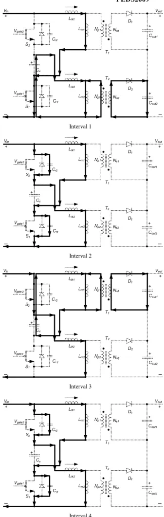
The idealized timing diagram of the proposed converter of Figure 2 is shown in Figure 3. Waveforms are not to scale. There are four time intervals:
• Interval 1: S
1is on and S
2is off. Current in L
kl1and L
m1is increasing. Energy is being stored in T
1core.
Current in L
lk2is decreasing while charging up C
c.
• Interval 2: Both switches are off (blanking time).
Current in L
lk1starts to decrease while charging C
r1. Because of the current and voltage polarity shown, current in L
lk2continues to increase negatively while discharging C
r2.
• Interval 3: S
1is off and S
2is on. Current in L
kl2and L
m2is increasing. Energy is being stored in T
2core.
Current in L
lk1is decreasing while charging up C
c.
• Interval 4: Both switches are off. Current in L
lk2starts to decrease while charging C
r2and current in L
lk1continues to increase negatively while discharging C
r1. B. Idealized current path diagram
The idealized current path diagram of the proposed converter of Figure 2 is shown in Figure 4. Referring to timing diagram of Figure 3, there are four time intervals:
• Interval 1: Energy is being stored in L
lk1and L
m1(core of T
1). The energy will be used during next Interval 3.
While energy that was previously stored in L
lk2is being clamped, energy that was previously stored in L
m2(core of T
2), is being transferred to the output stage.
• Interval 2: No energy is being transferred to output.
• Interval 3: Energy is being stored in L
lk2and L
m2. The energy will be used during next Interval 1.
different circumstances that would translate into cost, size and efficiency [10].
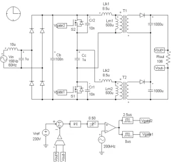
Simulations are done using the following assumptions:
• Duty ratio adjusted by an output voltage feedback proportional-integrator (PI) control loop.
• Diode voltage drop of one volt.
• MOSFET on resistance of 25m Ω.
• Isolation transformer turns ratio of N
p/N
s= 1/2.
Resistances of the windings are negligible.
• Other component values as noted on the schematic diagram of Figure 5.
In the circuit of Figure 2, because of the extra current path provided by the clamp circuitry, current in the leakage inductance of the isolation transformers can go negative. The circuit of Figure 5 uses a diode bridge at the input which would prevent negative current to the converter. As there might be operating conditions that charge needs to be returned to the input supply (bus pumping) and a rectifier bridge restricts that action, a capacitor needs to be added after the input diode bridge to provide a path for the negative current.
A. Waveforms of points of interest
Simulated voltage and current waveforms are provided in Figure 6 at the peak of input voltage with V
out= 230V and I
out= 2.2A. Waveforms are scaled.
The voltage across S
1also shows that the MOSFET operates with ZVZCS. The applied gating signal goes high while the body diode of the MOSFET is conducting (current through the switch is negative) and when the gating signal goes low, first current though the switch decays and then voltage across the switch increases. Also, it can be seen that the voltage across S
1is well clamped and there is a minimal overshoot or ringing, thus no extra snubber circuitry is needed for the switches.
Figure 6 also shows the input current which is (semi-) sinusoidal and is in phase with the input supply voltage.
B. Table and graph of values of interest
As the efficiency of a converter is becoming an important parameter to gauge its performance, the efficiency is not only reported at full load current but also at other load currents such as 25, 50 and 75 percent of the full load. Figure 5 has been simulated at different load currents to provide converter efficiencies presented in Table 1, running at the same conditions as above.
To investigate the effect of changing the input voltage
on operation of the converter, Figure 5 was simulated by
sweeping V
infrom 90V to 160V at a constant output
power of 500W and the results are shown in Figure 7. At low input voltages (V
in< 108V), duty ratio is saturated to 50% as a higher duty ratio is needed to maintain the output voltage at 230V, thus no control is available. At high input voltages (V
in> 113V), a lower duty ratio is needed to maintain the output voltage at 230V and thus ZVS operation is not performed and consequently, overall converter efficiency drops. The input operating voltage of 110V is inside the input voltage range that ZVS operation is performed (108V < V
in< 113V) where also the simulated efficiency is above 90%.
Figure 3. Idealized timing diagram of Figure 2
Interval 1
Interval 2
Interval 3
Interval 4
Figure 4. Idealized current path diagram of Figure 2
V. D ISCUSSION A. Inherent PFC operation
As power supply manufacturers are trying to sell their products in a global market, limiting the input current harmonics to the levels documented in IEC-6000-3-2 is recommended [11] [12]. Traditionally a PFC stage is put before a power converter stage, effectively putting two power stages in series. The two-stage approach has some disadvantages such as overall efficiency drop due to double conversion and higher cost. A single-stage approach merges the two separate power stages together, alleviating the above disadvantages [13].
If a single-stage PFC converter is working in discontinuous conduction mode (DCM), PFC functionality is automatically achieved [14]. Using DCM approach, additional input current sensing and current controller circuitry is not needed which would reduce overall complexity and cost. The complexity comes from the fact that the operating point of the PFC circuitry constantly changes as the instantaneous magnitude of the input AC voltage changes with time during each AC period [15]. Using this approach, current control loop and related stability difficulties are removed and thus only the output voltage has to be sensed and controlled. Operating in DCM also means that the inductor would have larger current swings, resulting in more resistive losses and a bigger filter at the input. This would make the discontinuous mode more appealing for lower power levels.
B. Challenges and limitations
Each output stage of the proposed converter has to use a single diode as shown in Figure 2 because the converter is based on flyback topology. A different type of output stage configuration, such as full diode bridge, creates a different current path that is not compatible with the requirements of flyback topology.
There are also other restrictions regarding the proposed design as follows:
• Because gating signals to the switches have same duty ratio and are shifted by 180 degrees, duty cycle needs to be restricted to a maximum of 50%
(40% considering 0.5µs blanking time at 200kHz to provide for the delay needed for ZVS operation).
• Since the proposed converter is based on flyback topology, voltage across switches during turn off is higher than the input voltage, as discussed in Section 2. Because this converter operates at lower than 50% duty ratios, this issue is not as severe as if it was operating at higher duty ratios.
Figure 5. Schematic diagram of the simulated converter
Table 1. Simulated values of Figure 5 at V
in= 110V, various P
outR
out( Ω) P
out(W) Efficiency (%)
106 500 93
141 375 84
212 250 74
424 125 66
104317.50 104320.00 104322.50 104325.00 104327.50 104330.00
Time (us) 0.0
-200.00 200.00
Figure 6. Simulated waveforms of Figure 5 at V
in=110V, P
out=500W (top) Currents in the transformer T
1,
(bottom) Switch S
1voltage and current
0 10 20 30 40 50 60 70 80 90 100
90 100 110 120 130 140 150 160
Vin (V)
percentage
No Control Zone
Efficiency
Duty Cycle
Figure 7. Simulated values of Figure 5 at various V
in, P
out= 500W
• At low duty cycles, both transistors are needed to be on for a shorter amount of time. Thus the time between when one switch is turned off and the other switch is turned on is increased. This will result in turning on a transistor while the window of opportunity for ZVS operation (see Section 2) has long been closed. Thus ZVS operation won’t be achievable at lower duty cycles. Similarly, at low output currents, because a lower current for a shorter amount of time is passing through the body diodes of the switches, the window of opportunity closes quickly and thus ZVS operation won’t be achievable at lower output currents either.
• If complimentary duty cycles were to be used, duty cycle D would be applied to one individual converter while (1−D) would be applied to the other. As the design is based on flyback topology, according to (2) at Ds other than 50%, one switch will see much higher voltage across it compared to the other one. As a result, C
cwill have a relatively high voltage swing resulting in excessive current through it, which makes this scenario of no use.
• If complimentary duty cycles were to be used, according to (1) at Ds other than 50%, each individual converter will have a different output voltage, thus the output stages can not be put in parallel. In this design, since the output stages are put in series, output voltages will add up to provide V
out. As D varies, V
outwon't be constant because:
⎟ ⎠
⎜ ⎞
⎝
⎛ + −
∝ −
D D D
D V
V
in
out