Ultraviolet Photodetectors Based on MgZnO Thin Films Grown by RF Magnetron Sputtering
Reporter: Jr-Shiang Shiau
Advisor : Prof. Jow-Lay Huang Prof. Chuan‐Pu Liu
1
2016.04.27
Outline
Introduction
Ultraviolet Photodetector
Materials
Experiment
Result and discussion
Characterization of ZnO and MgZnO thin films
Ultraviolet Photodetectors’ properties based on MgZnO films grown on silicon substrate
Conclusions
2
Ultraviolet Photodetector
Recent development in technology of wide bandgap semiconductors have stimulated up major interest in UV potential application.
The fundamental operating principle of all solid-state photosensitive devices is the same. A photon with sufficient energy interacts with a semiconductor crystal and create an electron-hole pair.
UV region of the electromagnetic spectrum: UVA for λ=400–320 nm; UVB for λ=320–280 nm ; and UVC for λ< 280 nm.
3
Light
Operating physics principle of PDs.
hν
hν
hν
Ozone depletion
Enhance photodetector performance
4
Device structure
MSM Schottky p-n junction
Piezo- phototronic
Schottky photodiode:
High response speed
Low dark current
High UV/dark contrast
Possible zero-bias operation
eVbi EF
eϕSB=e(ϕM-χ) Ev
Ec
Semiconductor Metal
Piezoelectricity Semiconductors Photon excitation
Wang, ZL. National Science Review;2013
Materials selection
5
Large tunable band-gap energy
Low cost
large exciton binding energy of 60 meV
Strong radiation hardness
High chemical stability
Environment friendly
MgO
ZnO MgO
Crystal Structure
Band gap 3.27eV 7.8eV
Lattice constant
a=3.2496 Å
c=5.2042 Å
a=4.212 Å
Ionic Radius 0.6 Å 0.57Å Melting point 1975 ℃ 3600 ℃
Density 5.606 g cm
-33.58 g cm
-3Molar mass 81.408 g mol
-140.304 g mol
-1E.R.Segnit. J. Am. Ceram. Soc.1964
Choopun, S. Appl. Phys. Lett.2002
Extending application
6
Gas sensors
Transparent electronics
Flame sensors
UV light emitters
Photodetector UV
SAW
Pressure sensors
Nanogene
-rator
Motivation
7
MgZnO is a potential material for optoelectronic applications and it is easy to synthesize. The large tunable band gap can fabricate the photodetector which is visible blind.
Material system
Promotion method
Piezo-phototronics provided a new rout to boost performance of photodetectors by applying external strain, which have been demonstrated on c-axial ZnO nanowire based MSM UV photodetectors.
Piezoelectricity
Semiconductors
Photon excitation
Piezo- phototronic
Experiment-Thin films deposition
8
Target Purity Mode Power
ZnO 99.99% RF 100W
Mg
0.3Zn
0.7O 99.99% RF 100W
Chamber pressure: <1×10
−5Tor
Working pressure: 4×10
−2Tor
Temperture: 25~250 ◦C
Gas flow: 30 sccm (Ar)
Time: 1~3hr
Thickness: 600 nm
Rotation speed: 15 rpm
Ar
RF Power Supply For ZnO & Mg0.3Zn0.7O Target
Halogen Lamp
Substrate
Ultrasonic bath for 10 min
Acetone
Isopropyl alcohol
DI water
Si
1cm 3cm
Experiment-Devices fabrication
9
250μm 150μm
2mm
Electrodes: Au
Thickness: 20 nm
Pairs: 12
Area: 91.5625mm2
Precision etching & coating system
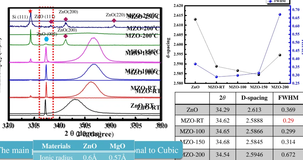
Figure 1. The θ–2θ X-ray diffraction pattern of ZnO and MgZnO films on Si with various temperature from 25 to 250 ℃.
Result and discussion 𝜃𝜃-2𝜃𝜃 X-ray diffraction
10
2𝜃𝜃 D-spacing FWHM
ZnO 34.29 2.613 0.369
MZO-RT 34.62 2.5888 0.29 MZO-100 34.65 2.5866 0.299 MZO-150 34.68 2.5845 0.314 MZO-200 34.54 2.5946 0.672
MZO-250 -- -- --
The main phase transform from Hexagonal to Cubic
Si (111)
ZnO (002) ZnO (111)
ZnO(200)
ZnO(220)
ZnO(200)
Materials ZnO MgO Ionic radius 0.6Å 0.57Å
EPMA- Electron Probe X– ray Microanalyzer
11
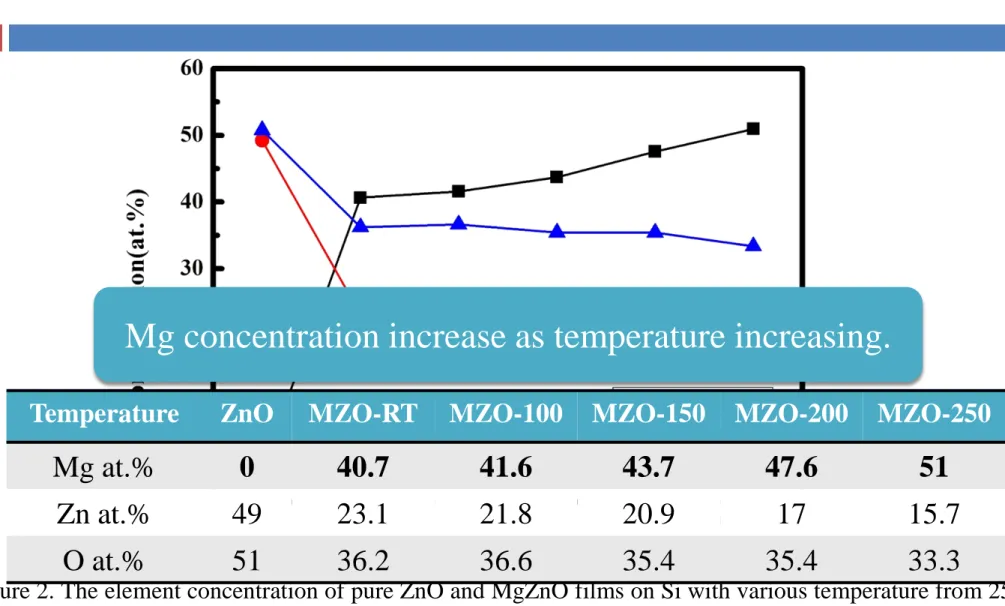
Mg concentration increase as temperature increasing.
Temperature ZnO MZO-RT MZO-100 MZO-150 MZO-200 MZO-250
Mg at.% 0 40.7 41.6 43.7 47.6 51
Zn at.% 49 23.1 21.8 20.9 17 15.7
O at.% 51 36.2 36.6 35.4 35.4 33.3
Figure 2. The element concentration of pure ZnO and MgZnO films on Si with various temperature from 25 to 250 ℃.
SEM- Scanning electron microscope
12
Pure ZnO Mg 40.7at.% Mg 40.7at.%
Nanorod like columnar thin films .
Figure 3. Cross-sectional and top-view SEM of pure ZnO and MgZnO films on Si with different Mg concentration.
Figure 4. Cross-sectional and top-view SEM of MgZnO films on Si with different Mg concentration.
SEM- Scanning electron microscope
13
40.7at.% 40.7at.%
Mg 43.7 at.% Mg 47.6 at.% Mg 51 at.%
Deposition rate reduce as temperature increasing
and causing Mg concentration increased.
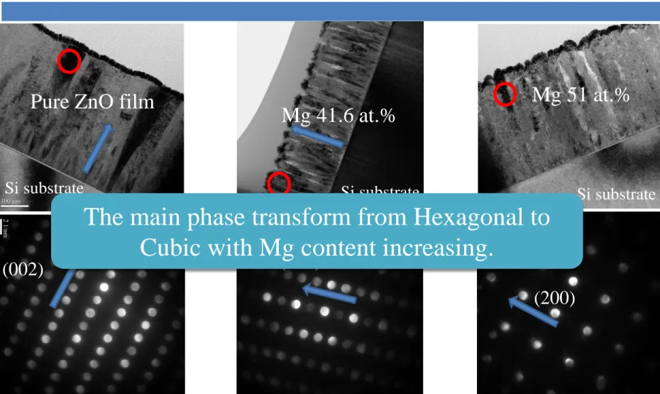
TEM- Transmission electron microscope
14
Si substrate
Pure ZnO film
(002)
Si substrate
(002)
Mg 41.6 at.%
(200)
Si substrate
Mg 51 at.%
The main phase transform from Hexagonal to Cubic with Mg content increasing.
Figure 5. Cross-sectional TEM bright-field image and nano beam diffraction patterns of pure ZnO and MgZnO films deposited on Sisubstrate at various Mg concentrations.
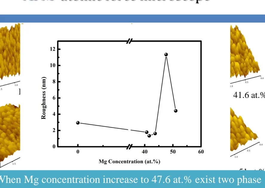
Figure 6. The AFM image of MgZnO films deposited on Si substrate at different Mg content .
AFM - atomic force microscope
15
Pure ZnO 40.7at.% 41.6 at.%
43.7 at.% 47.6 at.% 51 at.%
When Mg concentration increase to 47.6 at.% exist two phase
in the thin film causing the lattice distortion.
XPS -X − ray Photoelectron Spectroscopy
16
Figure 7. The XPS graphs of MgZnO thin films.
The intensity of Zn 2p decreased with Mg increasing and the
oxidation of thin films result the peaks shift to higher energy.
I-V Current–voltage characteristic
17
40.7at.%
41.6at.% 43.7 at.%
Photocurrent at bias+2V
Photocurrent was enhanced with the illumination intensity increased.
Mg 43.7at.% has the best photosensitivity.
Mg 40.7 at.% Mg 41.6 at.% Mg 43.7 at.%
325nm Laser
I
ph=(I
tot-I
dark)
Figure 8. The I-V curves of MgZnO films deposited on Sisubstrate at different Mg content.
18
Xiaonan Wen. Adv. Mater. 2013.
Piezo-phototronic effect
ln 𝐼𝐼 𝜀𝜀 𝐼𝐼 ⁄ 0 = −𝑞𝑞 ∆Φ
𝑏𝑏⁄ 𝑇𝑇 𝑘𝑘
𝐼𝐼(𝜀𝜀), I(0),𝑞𝑞 , k, T are current with and without strain, elementary charge, Boltzmann constant, absolute temperature, respectively.
Compressive Tensile
Tensile Compressive
Figure 9. The I-V curves of MgZnO (Mg = 43.7at.%) films .
Photoresponse
19
R
p=I
ph/P
opt=(I
tot-I
dark)/P
optStart λ 280nm
End λ 400nm
Interval λ 1 nm Delay time 0.1 s Applied bias 4-9V
Maximum response:295nm 4.5A/W at 9V Cut off wavelength:310nm
(1) the large surface-to-volume ratio and the presence of deep level surface trap states in NWs greatly prolongs the photocarrier lifetime.
(2) the reduced dimensionality of the active area in NW devices shortens the carrier transit time.
Electron hole pairs generated O2+ e- → O2- (ad) Oxygen desorption h++ O2- (ad)→ O2 (g)
Two main factors contributing to the high photosensitivity
C. Soci. Nano Lett. 2007
.
Figure 10. The responsivity of MgZnO (Mg = 43.7at.%) films.
Conclusions
20
High quality Mg
xZn
1-xO thin films without buffer layer exist the preferred orientation (002) direction have been grown on silicon substrate by RF- magnetron sputtering.
The Mg content x (40.7–51 at.%) can be controlled by changing substrate temperature (25-250 ℃) and the phase transformation from hexagonal to cubic phase happen when substrate temperature is increased to 200 ºC (Mg 47.6 at.%).
A visible-blind photodetector had been fabricated with IDT-Schottky type photodetector MgZnO (43.7 at.%) have the best performance of sensitivity and photo-response.
The photodetector responsivity was further increased through the piezo-
phototronic effect by an order of magnitude under simultaneous
application of load and illumination.
21
Thank you For your attention
This project was financially supported by the Ministry of Science and
Technology of the ROC under contract No. MOST 104-2221-E-006-032-MY3.
Thin films growth condition
22
23
Growth
technique Substrate Electrod
es Devic types e
Light of detectio
n
Respons ivity (A/W)
Applie d bias MgZnO (W)
(annealed 673K)
sputtering RF- quartz Ni/Au MSM 305nm 2.133 10V
Mg0.49Zn0.51O
(W) Reactive
magnetron cosputtering
ZnO Au MSM 260nm 0.304 10V
Mg0.1Zn0.9O (annealed 573 (W)
K)
magnetron RF sputtering
SiO2/n-Si Ni/Au MSM 340nm 0.2 0V
Mg0.33Zn0.67O
(M) Molecular
beam epitaxy
a-sapphire Au MSM 330nm 32 10V
Mg0.34Zn0.66O
(W) RF
magnetron sputtering
Si Al MSM 330nm 34.02 5V