A study of biasing crystallized on structural and electrical properties of ZITO film
Kuan-Jen Chen1, Fei-Yi Hung2*, Shoou-Jinn Chang1, Sheng-Po Chang1, Zhan-Shuo Hu3, Kuang-Wei Liu3,
1Institute of Microelectronics & Department of Electrical Engineering, Center for Micro/Nano Science and Engineering, National Cheng Kung University, Tainan 701, TAIWAN
2Institute of Nanotechnology and Microsystems Engineering, Center for Micro/Nano Science and Engineering, National Cheng Kung University, Tainan 701, TAIWAN
3Institute of Electro-Optical Science and Engineering,Center for Micro/Nano Science and Technology, National Cheng Kung University, Tainan 701, TAIWAN
* Corresponding author: [email protected]
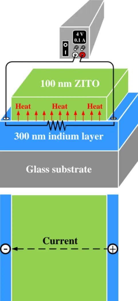
The Zn-In-Sn-O (ZITO) film was deposited onto the indium/glass substrate by co-sputtering system using RF power of 80 W (for ZnO target) and DC power of 40 W (for ITO target). The resistivity and electron mobility of as-grown ZITO film was 3.08×10⁻⁴ Ω*cm, 13.9 cm2/V*s, respectively. To understand the contribution of biased crystallized on the characteristics of ZITO film, the electrical current method was used by DC power supply. Figure 1 shows the schematic illustration (Cross-section view and top view) of biased crystallized for ZITO film. As the voltage of 4 V biased upon the indium layer (Figure 2), the resistivity gradually reduced and the carrier concentration increased which associated with the Joule heat or electro-migration effects. Also, the Joule heat and electro-migration affected the ZITO crystallization (Figure 3). As a result, the indium was diffused into upper ZITO film by biasing induced Joule heat resulted in the deterioration of ZITO crystallization.
300 nm indium layer
Glass substrate
Heat
100 nm ZITO
Heat Heat
4 V 0.1 A
- Current
Figure 1 The schematic illustration of biased crystallized for ZITO film.
1021 1022 1023 1024 1025
0 1 2 3 4
As-grown 20 30
Biasing time (min) Resistivity (×10-4 Ω∗cm)
10 10-2
10-1 100 101
Mobility (cm2 / V*s)
Resistivity Mobility
Carrier concentration
Carrier concentration (1/cm3 )
Figure 2 The relation of biasing duration and electrical properties (resistivity, mobility and carrier concentration).
20 30 40 50 60 70 80
S u b . I n l a y e r Z I T O f i l m
In2O3
Biasing (4V)
c
(202) (211) (103) (200) (112)
(222) (110) (321)c
Intensity (a.u.)
2θ (degree)
(002) As-grown
In
Figure 3 XRD patterns of as-grown ZITO film and ZITO film with biasing of 4 V.