Morphology and Phase Transformation at a Solder Joint in a Solid-State Reaction
Tao-Chih Chang, a,z Min-Hsiung Hon, a and Moo-Chin Wang b
a
Department of Materials Science and Engineering, National Cheng Kung University, Tainan 70101, Taiwan
b
Department of Mechanical Engineering, National Kaohsiung University of Applied Sciences, Kaohsiung 80782, Taiwan
Morphology and phase transformation at a solder joint of the Sn-9Zn-xAg lead-free solders and Cu substrate in a solid-state reaction have been investigated in this study. The Cu
6Sn
5intermetallic compound is formed at the Sn-9Zn/Cu interface but the Cu
5Zn
8layer decomposes as aged at 180°C, which causes microvoid formation at the solder joint. However, microvoid formation is suspected at the Sn-9Zn-xAg/Cu interface due to the Ag
3Sn formation. A bistructural Cu
6Sn
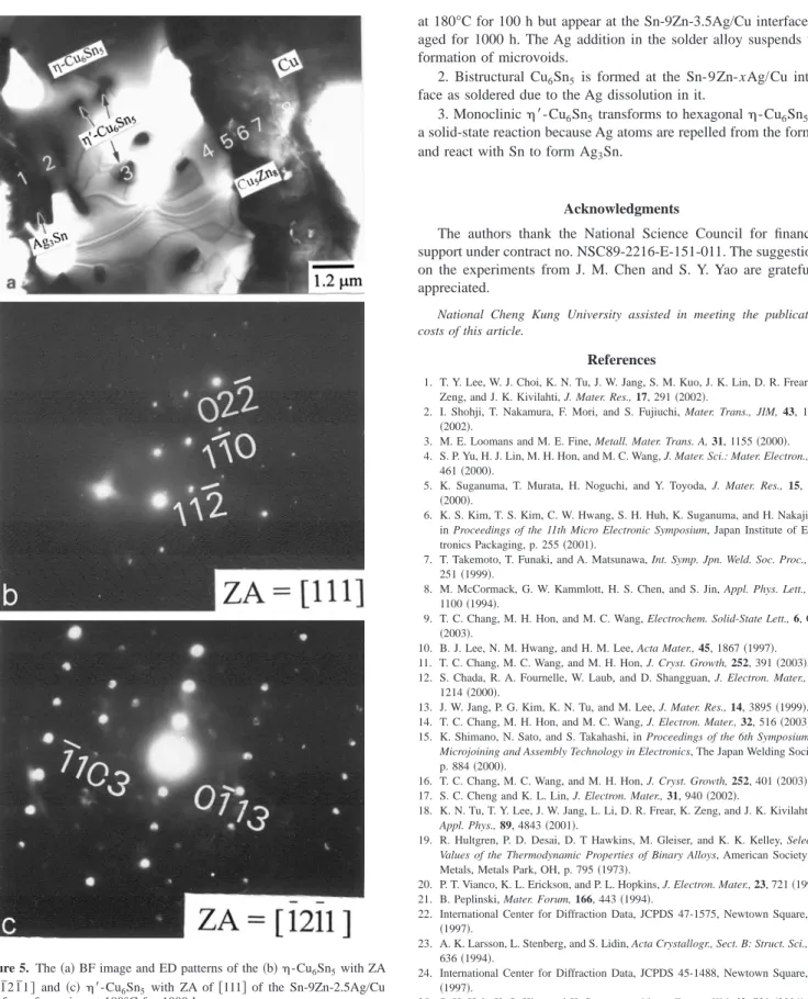
5layer is found at the Sn-9Zn-xAg/Cu interface after soldering due to the Ag dissolution in it. As aged at 180°C, the Ag is repelled from the ⬘ -Cu
6Sn
5and makes it transform to the -Cu
6Sn
5.
© 2003 The Electrochemical Society. 关DOI: 10.1149/1.1635772兴 All rights reserved.
Manuscript submitted June 16, 2003; revised manuscript received July 11, 2003. Available electronically December 15, 2003.
Due to the toxicity of Pb, various lead-free solders have been used to substitute for 63Sn-37Pb solder alloy to be an interconnect- ing material in electronic packaging, such as Sn-3.5Ag, Sn-9Zn, Sn-3.5Ag-0.9Cu, and Sn-8.55Zn-0.45Al. 1-4 However, some prob- lems like high melting point of Sn-3.5Ag and Sn-3.5Ag-0.9Cu, oxi- dation of Sn-9Zn, and Kirkendall void formation at the solder joint must be resolved before these alloys can be used in practice.
The formation of microvoids at the Sn-9Zn/Cu interface during aging has been observed by Shohji et al. 2 and Suganuma et al. 5 They have shown that microvoids are formed at the solder joint after Cu 6 Sn 5 appears at the interface, which deteriorated solder joint re- liability. However, the formation mechanism of the microvoids is not clear although Suganuma et al. 5 demonstrated that microvoids are due to the inferior wettability between the Sn-9Zn solder alloy and Cu substrate. But Kim et al. 6 have proposed that the formation of the microvoids is attributed to the diffusion of Sn.
Sn-9Zn-xAg solder alloys are promising materials to take the place of 63Sn-37Pb solder alloy because of better wettability and mechanical properties than Sn-9Zn solder alloy, 7,8 and Kirkendall void formation at the solder joint are inhibited as aged. 9 However, the effect of Ag addition on the formation of microvoids has not been discussed in detail. The objectives of this study are to (i) discuss the formation mechanism of microvoids, (ii) hinder the for- mation of microcracks at the Sn-9Zn/Cu interface by Ag addition, and (iii) investigate phase transformation at a solder joint.
Sn-9Zn-xAg lead-free solders were made with pure Sn, Zn and Ag with x of 0, 0.5, 1.5, 2.5, and 3.5 wt %. The pure metals were degreased and deoxidized in 5 wt % NaOH and 5 vol % HCl solu- tions, respectively, and rinsed in deionized water after each step. The substrate was an oxygen-free, high conductivity Cu plate 60 ⫻ 20
⫻ 2.5 mm. The cleaning process for the Cu substrate was con- ducted like the pure metals. After pretreating, the Cu substrate was immersed in a 3.5 wt % DMAHCl solution 共3.5 wt % dimethylam- monium chloride and ethanol as a solvent 兲 for 10 s to enhance the surface activity of the Cu substrate and avoid reoxidizing of the surface. Afterward, the Cu substrate was soldered in the melted Sn-9Zn-xAg lead-free solders at 250 and 350°C for 10, 20 and 30 s, respectively. The temperature of 250°C corresponds to the practical reflowing temperature. However, a higher soldering temperature of- fered better wettability of solder alloy on Cu substrate, so samples soldered at 350°C for 30 s were aged at 180°C for 100, 250, 400, 750, and 1000 h, respectively. Phase transformation of -Cu 6 Sn 5 to
⬘ -Cu 6 Sn 5 at 170°C can be prevented under the chosen tempera-
ture. The morphology of the Sn-9Zn-xAg/Cu interface was ob- served by a scanning electron microscope 共M-SEM, JXA-840, JEOL, Japan 兲 and the chemical composition of the intermetallic compounds 共IMCs兲 formed at the interface was determined by an energy dispersive spectrometer 共EDS, AN10000/85S, Links, U.K.兲.
Twenty values of the IMC thickness were estimated and averaged. A transmission electron microscope 共TEM, HF-2000, Hitachi, Japan兲 with an EDS 共Voyager 1000, Noran兲 was used to observe the inter- face and electron diffraction 共ED兲 was utilized to identify the struc- ture of the Cu 6 Sn 5 IMC layer.
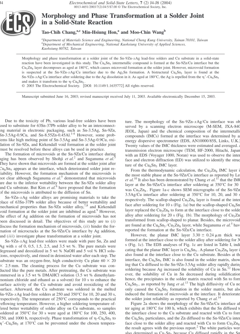
From the thermodynamic calculation, the Cu 5 Zn 8 IMC layer is the most stable phase at the Sn-9Zn/Cu interface as reported by Lee et al. 10 It also has been demonstrated by Chang et al. 11 that the IMC layer at the Sn-9Zn/Cu interface after soldering at 350°C for 30 s was Cu 5 Zn 8 . Figure 1a-c shows SEM micrographs of the Sn-9Zn- 3.5Ag/Cu interface after soldering at 350°C for 10, 20, and 30 s, respectively. The scallop-shaped Cu 5 Zn 8 layer is found at the inter- face after soldering for 10 s 共Fig. 1a兲 but the scallop-shaped Cu 6 Sn 5
layer replaced the Cu 5 Zn 8 to form at the interface close to the solder alloy after soldering for 20 s 共Fig. 1b兲. The morphology of Cu 5 Zn 8 transformed from scallop-shaped to planar. Besides, the microvoids are found at the Cu 6 Sn 5 /Cu 5 Zn 8 layer, while Suganuma et al. 5 have reported the formation at the Sn-9Zn/Cu interface.
However, the planar IMC layer 3.30 ⫾ 0.24 m thick was formed at the interface close to the solder alloy after soldering for 30 s 共Fig. 1c兲. The EDS analyses of Fig. 1c are listed in Table I, indi- cating that the planar IMC layer is Cu 6 Sn 5 . A planar Cu 5 Zn 8 layer is also found at the interface close to the Cu substrate. Besides at the interface, the Cu 6 Sn 5 IMC is also found in the solder matrix, show- ing that Cu diffused to the Sn-9Zn-3.5Ag solder alloy rapidly during soldering because Ag increased the solubility of Cu in Sn. 12 How- ever, the solubility of Cu in Sn decreased during solidification, hence, the precipitates in the solder matrix reacted with Sn to form Cu 6 Sn 5 , as reported by Jang et al. 13 The high diffusivity of Cu not only caused the Cu 6 Sn 5 formation in the solder matrix, but also induced the formation of microvoids at the interface. It deteriorates the solder joint reliability as reported by Chang et al. 14
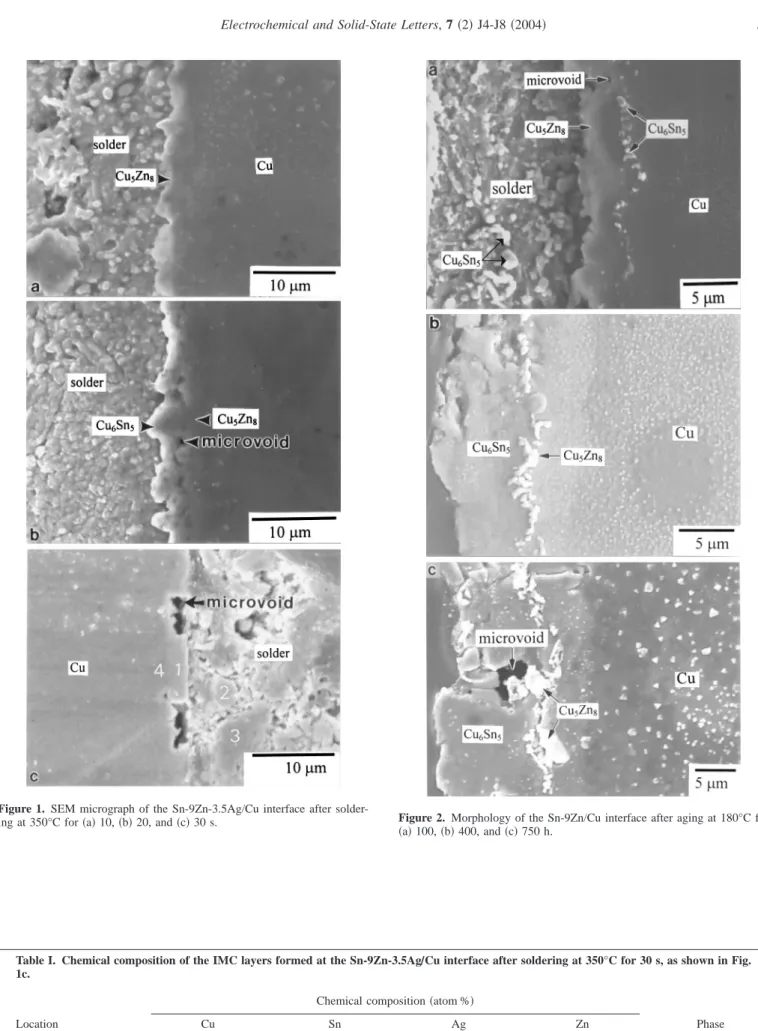
Figure 2a shows the morphology of the Sn-9Zn/Cu interface af- ter aging at 180°C for 100 h, which exhibits that the Sn diffused to the interface close to the Cu substrate and reacted with Cu to form the Cu 6 Sn 5 particulates, and the Zn diffused to the Sn-9Zn/Cu inter- face close to the solder alloy and reacted with Cu to form Cu 5 Zn 8 , the result agrees with the previous report. 2 The white particles were also determined as Cu 6 Sn 5 because Cu diffused rapidly in the Sn- 9Zn solder alloy 2 and reacted with Sn to form Cu 6 Sn 5 . Yu et al. 4
z