This content has been downloaded from IOPscience. Please scroll down to see the full text.
Download details:
IP Address: 140.113.38.11
This content was downloaded on 28/04/2014 at 16:36
Please note that terms and conditions apply.
Room-temperature selective growth of dielectric films by liquid-phase deposition
View the table of contents for this issue, or go to the journal homepage for more 1994 Semicond. Sci. Technol. 9 1250
(http://iopscience.iop.org/0268-1242/9/6/015)
Semicond. Sci. Technol. 9 (1994) 1250-1254. Printed in the UK
Room-temperature selective growth
I
of dielectric films
by
liquid-phase
deposition
Ching-Fa Yeh and Chun-Lin ChenDepartment of Electronics Engineering & Institute of Electronics, National Chiao
Tung University, 1001 Ta Hseuh Road, Hsinchu, Taiwan
Received 14 December 1993, accepted for publication 2 March 1994
Abstract. In multilevel interconnection processes, because thermal stress affects device characteristics and wiring reliability, low-temperature deposition has been required for interlayer dielectrics (SiO,). This research investigated high growth rate and selective growth conditions of room-temperature interlayer dielectrics
formed using the liquid-phase deposition method. The dependence of deposition
rate on growth temperature and H,B03 concentration is confirmed, and a concentration of 3.8 mol I-' of H,SiF, is used to achieve a high deposition rate of
1250 A h - ' . The degree of supersaturation of silica of the immersing solution is found to define three ranges of growth conditions: the nondeposition range, selective deposition range, and conformal deposition range. A selective
deposition model is proposed to clarify the mechanism of room-temperature selective SiO, growth.
1. Introduction
Interlayer dielectric film formation technology is
essential^
for the fabrication of multilevel interconnections in ULSI. Low-temperature deposition has been required for multilevel interconnection interlayer dielectrics because thermal stress affects device characteristics and wiring reliability. This problemis
likely to become more serious in future deep-submicrometre interconnections. Low- temperature deposition techniques using organic sources such as Tms-ozone APVCD, H20-mOs PECM, and biased ECR CM) have been investigated for use in fabricating multilevel interconnections [I-41. However, all of these techniques share a fatal drawback it is impossible to reduce the temperature significantly, because a substrate temperature above 300 "C is required for polymerization and dehydration. Therefore deposition at a lower temperature without residual OH has been difficult to achieve. Recently, researchers have attempted to develop room-temperature interlayer dielectric deposition tech- nology for deep-submicrometre multilevel interconnec- tions [SI. In particular, techniques providing selective growth capability for complete planarization by using the liquid-phase deposition (LPD) method[6,
71 have attracted much attention. This type of method is simple, and the equipment required is very inexpensive. However, to date the deposition rates achieved have been so low that this type of method remains impractical for industrial use. Thus the critical issue at this juncture is whether or not a technology can be developed to supply a high growth rate and selective growth. In addition, room- 0268-1242/94/061250 t o 5 $19.50 @ 1994 IOP Publishing Ltd.- temperature selective growth will become suitable for a wider range of applications,
if
the range of growth conditions and the growth mechanism can be clarified. This research investigated room-temperature high growth rate and the range of selective growth conditions using the LPD method.2. Experiment
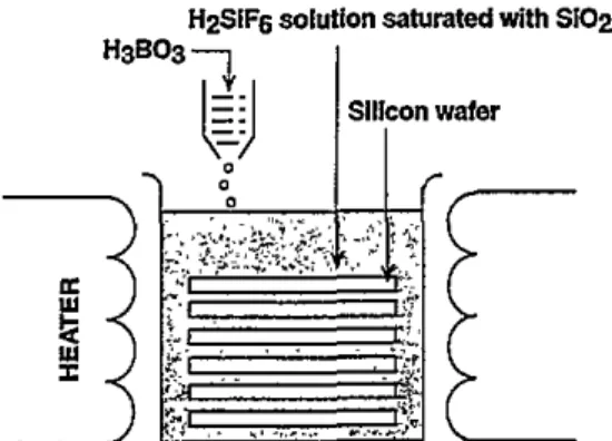
The apparatus used in this research is illustrated in the schematic diagram in figure 1. The room-temperature control bath was adjusted to the desired reaction temperature (RT) RT 0.01 "C. The immersing solution was prepared by dissolving highly purified silica particles (SiOJ in H,SiF, at 23 "C to obtain a saturated solution
HzSIF6 solution saturated with SI02 I
Figure 1. A schematic diagram of t h e apparatus used for liquid-phase deposition of dioxide.
RT selective dielectric film growth by LPD
of 4.0 mol 1-' with silica, followed by filtering to remove undissolved silica. To obtain a supersaturated state with SO, in the immersing solution, a boric acid solution^
(0.1 mol I-') was added and the solution was stirred for 20 min. The SO, film was then prepared by immersing Si wafers in the solution. The film thickness was adjusted by controlling the immersion time. The chemical reaction for SiO, growth can be represented by the following two equilibrium processes in the treatment solution. The one process is in the hydrofluosiiicic acid as shown in equilibrium (1):
H2SiF6
+
2H,O ~t 6HF+
SO,. (1) In this equilibrium, the addition of SiO, wiii lead the shift from right to left. Therefore the treatment solution comprising hydrofluosilicic acid saturated with silica may include hydrofluoric acid which was minimized in equilibrium (1). However, this equilibrium may be changed by the addition of boric acid to the treatment solution. Normally boric acid easily reacts with hydro- fluoric acid as shown by equilibrium (2):H,BO3
+
4HF Ft BF;+
H,O++
2H20. (2) Accordingly, the addition of boric acid to the treatment solution leads to the consumption of the minimized hydrofluoric acid and brings about a transient state supersaturated with SO, in equilibrium (1). Such supersaturation of SiO, shifts the equilibrium process (1) from left to right following a silica deposition mainly on the substrate.The concentration of H,SiF6 and boric acid (H,BO,) and the temperature can inffuence the degree of super- saturation and the rate of SiO, growth. For an H,SiF, concentration of 2.0 mol 1-l: the deposition rate has been reported to be about 80-300Ah-', depending on temperature [7]. According to ourinvestigations, however, at this concentiation LPD S O2 can hardly be produced at all. Consequently, in this study a concentration of 3.8 mol 1-' of H,SiF6 was used to enable us to investigate high growth rate and selective growth capability.
Growth of SO, films was performed mainly on Si wafers at constant RT. Firsf to study the dependence of the growth rate on temperature, various RT (35, 40 and 45 "C) were selected, and an H,BO, concentration of 1.46 x lO-'moll-' was adopted. Next, to study the dependence of the deposition rate on H,B03 concen- tration, the quantity of H3B03 was varied in the range
of (1.46-2.55) x 10-2mol 1-', while the bath temperature was fixed at 35°C. Ellipsometry, a sensitive tool for monitoring the film thickness ( t ) and refractive index (A') of a dielectric film, was used. To examine the effect of deposition conditions on chemical stability, the P-etch rate using the solution (48% H F 70% HNO,: H 2 0 = 3 2 6 0 in volume) at room temperature was also evaluated. To investigate the conformability and the property of selective growth, the LPD SO, growth profiles, which were formed on the double-layer structure of tungsten interconnection lines covered with positive photoresist, were inspected using scanning electron microscopy (sm4).
3. Results and discussion
3.1. Growth temperature dependence
We investigated the growth of LPD SiO, film at 35 "C in a solution with 3.8 moll-' of H2SiF6 and 1.46 x
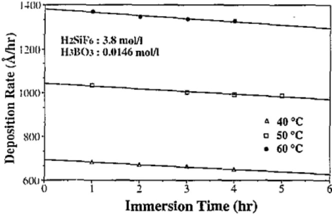
lo-' mol 1-' of H3B03. Fourier transform infrared spectroscopy (FTIR) of an as-deposited LPD Si02 film indicates intensive peaks around 1092.5 cm'-' and 927.3 cm-' due to the stretching vibration of Si-0-Si bonds and Si-F bonds respectively. This obviously shows that the LPD SiO, film is rich in Si-0-Si bonds and has an orderly silica network and consequently good chemical stability. The refractive index of the LPD SO2 is shown to be 1.43. These chemical properties reveal that the LPD SiO, film is similar to the film grown in 2.0 mol 1-' reported in [lo]. The growth of SO2 is linearly dependent on the immersion time, and the deposition rate (DR) can be easily obtained. We also found that, as shown in figure 2, the DR decreased slightly with immersion time owing to the consumption ofboric acid with increased immersion time. Because the chemical reaction for LPD SiO, growth is dependent on temperature, as shown in equilibrium processes (1) and (2), it is possible that the DR can be controlled by changing the solution temperature. As shown in figures 2 and 3, the deposition rate indeed increases with temperature. Comparing our results with the deposition rates reported in [7], we find that the new
conditionof3.8mo11-'ofH,SiF6and 1.46 x 10⁻²moll-' of H3B03 adopted in this research apparently enhanced the rate of growth of LPD SiO, film.
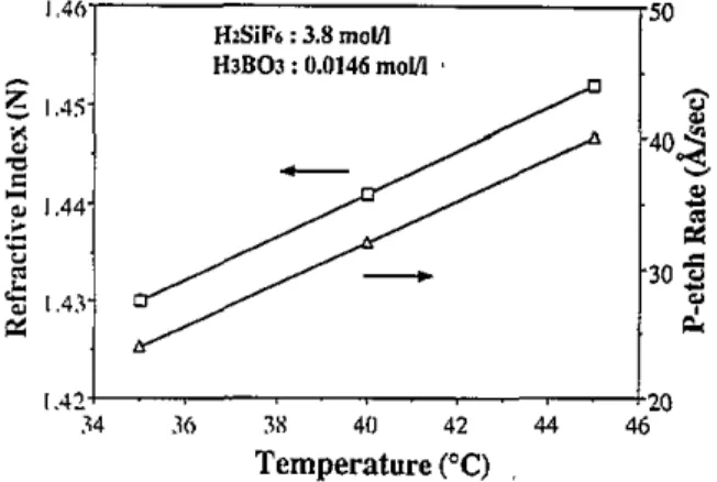
From FTIR evaluation, we have confirmed that an increase of growth temperature had no effect on the chemical composition of the LPD SiO, films. However, as depicted in figure 4, the refractive index of the dielectric films increases linearly with the growth temperature. This result indicates there must be a slight difference in the structure offilms grown at different temperatures. In fact, the chemical stability in terms of the P-etch rate was evaluated for all the LPD SiO, films. As shown in figure 4, the film grown at higher temperature has a higher P-etch rate and thus seems to be less dense. However, for LPD SO,, a low P-etch rate (24
A
s-') may also be due to its superior chemical stability.Immersion Time (hr)
Figure 2. Dependence of deposition rates on immersion
time at different temperatures for the solution with 3.8 mol I-' of H,SiF6 and 0.0146 mol I-' of H,B03.
Ching-Fa Yeh and Chun-Lin Chen
..I, I
, ..-_
25 311 25 40 45 50
Tempersturc('C)
Figure 3. Dependence of deposition rate on solution temperature for the solution with 3.8 mol I-' of H,SiF, and 0.0146 mol I-' of H,BOw For comparison, the deposition rate obtained by Nagayama et a/ [7] for the solution with
2 mol I-' of H,SiF, and 0.024 mol I-' of H,B03 is also shown,;
HiSilia : 3.8 moffl H 3 8 0 3 : 0.0146 mo!A '
e
t
Figure 4. Relationship of the refractive index a n d the
P-etch rate to the growth temperature for dielectric films prepared in t h e solution with 3.8 mol I-' of H,SiF, and 0.0146 mol I-' of H,BOp
3.2. H3B0, dependence
Besides using a high concentration (3.8 moll-') of H,SiF, solution, an alternative method of achieving
a
high DR is to increase the concentration of H3B03i thereby increasing the supersaturated degree of silica. As depicted in figure 5, the deposition rate is greater than600 A h- ' when the concentration of H3B03 is over
H3BO3 ( X I 0 5 mom)
Figure 5. Relationship of deposition rate to H3B03 concentration at 35 'C for t h e solution with 3.8 mol I - ' of H,SiF,. 1252
-.
.- L1.42 1.4 1.11 1.S 2.0 2.2 2. 4. 2.6 H3B03 (xl0-2 mom)Figure 6. Relationship of the refractive index and the P-etch rate to H3B03 concentration at 35 "C for the solution
with 3.6 mol I-' of H,SiF,.
1.46 x moll-', and it increases to 1250
A
h - l at a concentration of 2.548 x lo-' mol 1-'. In this high-DR region, we again confirmed from FTIR evaluation that no compositional alterations occurred in the as-grown films. However, as depicted in figure 6, the refractive index ( N ) of the dielectric f i b sshows an
increasing dependence on the concentration of H3B03. This result also implies that there must be a difference in the structure of the LPD Si02 films grown in solutions with various degrees ofsupersaturation. This can be corroborated by P-etch testing for these films. As depicted in figure 6, the film grown in a more supersaturated solution appears less dense, because of its increased P-etch rate.
3.3. Selective growth
In a previous experiment [ll]. we found that the conformal deposition could be easily carried out with 2.0 mol I-' H,SiF, solution. However,
we
failed to achieve selective growth with a solution of this concen- tration. After the concentration of the solution was increased to 3.8 mol 1-I, experiments with both temper- ature and H,BO, concentration as parameters revealed that there exist a range of degrees of supersaturation inwhich selective growth of LPD Si02 can be carried out. As shown by the two curves in figure 7, in which the x
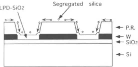
axis represents the growth temperature and the y axis represents the concentrations of H3B03, there are three ranges: the non-deposition range, the selective deposition range and the conformal deposition range. These ranges were determined by SEM cross-sectional inspection of all
the LPD SiO, growth profiles on the double-layer structure of photoresist/tungsten lines (figure 8(u)). Conformal deposition means that the deposition occurs all over the surface, including photoresist as illustrated in figure 8@), while selective deposition (figure 8(c)) means that the deposition occurs only on the substrate (in this case, SiO,). In the selective deposition profiles, there is a rounded shape at both edges of every space h e . This will be explained below using a selective growth model. As for non-deposition, LPD SiO, is not grown; in some cases the original SiO, substrate or the side-walls of tungsten interconnection have been etched (figure 8(d)).
RT selective dielectric film growth by LPD
At higher H , B 0 3 concentration, because the reaction rate of reaction (2) increases with temperature, the supersaturated degree of silica also increases with temperature. Thus a lower concentration of H,BO, is required to achieve conformal deposition at higher temperatures. In the conformal deposition range shown in figure 7, the supersaturated degree of silica is sufficiently high for both photoresist and substrate, hence the LPD Si02 grows easily all over both surfaces conformally. At a lower H,BO, concentration (< 0.868 x
l o - 2 mol I-') in the non-deposition range, the super- saturated degree of silica is too low to deposit silica. While the saturated H,SiF6 solution evaporates at room temperature, the concentration of the solution will decrease. In this case, the higher the temperature is, the lower the H2SiF6 solution concentration will be, so
the degree of supersaturation is too low to form silica. Occasionally the reverse reaction to (1) occurs and the oxide substrate is etched. Thus, it is essential to add more boric acid to increase the degree of supersaturation at high temperatures. In the selective deposition range, owing to the sufficiently high degree of supersaturation, which is adequate for LPD S i 0 2 growth on the substrate rather than on the photoresist, selective growth of LPD SiO, on the substrate against the photoresist was achieved.
Temperature ("C)
Figure 7. Three condition ranges, including (i) conformal deposition, (ii) selective deposition, and (iii) non- deposition, defined by the two deposition key factors of growth temperature and H,B03 concentration.
3.4. Selective growth model
Why selective growth of LPD Si02 occurs under the conditions in the selective deposition range is an important question. Before we attempt to formulate a model to explain our findings, two facts have to be emphasized. One is that the main difference between the three deposition ranges depicted in figure 7 lies in the degree of supersaturation of the immersing solution. The other fact is that whether or not LPD Si02 growth occurs on a surface is determined by the chemical structure of the surface, such as the organic polymer of the photoresist or the inorganic silicon dioxide. On the basis of these two facts, we suggest that a surface composed of a different material requires a solution with a different degree of supersaturation of SiO, for LPD SiO, deposition.
If an immersing solution is sufficiently supersaturated with SO2, silica will first be segregated throughout the solution; then it may react with the surface and be deposited on the surface by stabilized bonds. If the reaction energy owing to the surface chemical structure is not high enough to overcome the activation energy, segregated silica will migrate. If deposition occurs, owing to the lack of strong bonds the chemical structure of the film will be essentially different from that of film with strong bonds. As an example of this difference in chemical structure of the surface, the cross-sectional view in figure
8(h) clearly indicates that the structures of as-deposited
film on photoresist and substrate dioxides are different from each other. Accordingly, a selective deposition model can be proposed. In the selective deposition range, segregated silica can easily bond with substrate dioxide 1253 Figure a. SEM cross-section views of LPD SiO, profiles
prepared on the double-layer structure of photoresist/ tungsten line. (a)Typical representative view, (b) conformal deposition, ( c ) selective deposition and (d) non-deposition.
(b), (c) and (d) correspond to the three condition ranges
Ching-Fa Yeh and Chun-Lin Chen
deposition model proposed here should also help to clarify the mechanism of room-temperature selective deposition.
Acknowledgments
This study was supported by the National Science Council, Republic of China, under contract number NSC XI-0404-E-009-122.
Figure 9. A model f o r selective LPD SiO, growth.
and deposition with uniform structure occurs, while silica hardly bonds with the polymer surface at all but, as illustrated in figure 9, surface migration will occur. Thus the deposition rate at both edges of each space-line is high, and a rounded deposition shape occurs.
References
[I] lkeda Y, Numasawa Y and Sakamoto M 1990 J . Electron. Mater. 19 45
[2] Kotani H, Matsuura M, Fuji A, Genjou H and Nagao S 1989 IEDM Tech. Diq. 669 [3] Hatanaka M, Mizushima Y, Hataishi 0 and
Furumura Y 1991 IEEE Int. VLSI Multileuel
Interconnection Con$ (New Y o r k IEEE) p 435 [4] Pai C S, Miner J F and Foo P D 1991 IEEE Int. VLSI
Multileuel Interconnection Conf (New York IEEE) 4. Conclusion
This study has investigated the room-temperature p 442 selective growth conditions of LPD SOz. The dependence
of deposition rate on growth temperature and H,BO, concentration indicates that a high deposition rate can easily be obtained using a 3.8 mol 1-' H,SiF, immersing solution. We have shown that both growth temperature and H,BO, concentration have an important effect on the chemical properties of the LPD SOz deposited. The degree of supersaturation of silica of the immersing solution has been found to determine three ranges of deposition behaviour: the non-deposition range, selective deposition range, and conformal deposition range. Our results should be instructive in attempts to achieve room-temperature formation of planarized interlayer dielectrics for multilevel interconnections. The selective
[SI
HommaT,KatohT,YamadaY,ShimiruJand M u r a o Y 1990 IEEE VLSI Technology Symp. (New York:IEEE) p 3
161 Homma T and Murao Y 1991 I E D M Tech. Dig. 289
171 Nagayama H, Honda H and Kawahara H 1988
J . Electrochem. Soc. 135 2013
[8] Deki S 1989 56th Spring Meeting, Japan. Electrochrm. Soc. (Tokyo: Japan. Electrochem. Soc.) p 18 191 Deki S 1988 56th Spring Meeting, Japan. Chem. Soc.
(Tokyo: Japan. Electrochem. Soc.) p 751
cl01 y e h
c
F, Chenc
L, H~~~~ pc
and ~i~s s
1992 Proc. Ann. Con$ Chinese Society for Materials Science (Taipei Chinese Society for Materials Science) p 246Electron Devices and Materials Symp. (Taipei: IEEE) p 489