High-temperature threshold characteristics of a symmetrically graded InAlAs/ In
xGa
1−xAs/ GaAs metamorphic high electron mobility transistor
C. S. Leea兲
Department of Electronic Engineering, Feng Chia University, 100 Wenhwa Road, Taichung, Taiwan 40724, Republic of China
Y. J. Chen
United Microelectronics Corporation, Tainan Science-Based Industrial Park, Hsin-Shi, Tainan County, Taiwan 744, Republic of China
W. C. Hsu, K. H. Su, J. C. Huang, and D. H. Huang
Institute of Microelectronics, Department of Electrical Engineering, National Cheng-Kung University, 1 University Road, Tainan, Taiwan 70101, Republic of China
C. L. Wu
Transcom Inc., 90 Da-Shun 7th Road, Tainan Science-Based Industrial Park, Hsin-Shi, Tainan County, Taiwan 744, Republic of China
共Received 30 December 2005; accepted 5 May 2006; published online 30 May 2006兲
High-temperature threshold characteristics of a symmetrically graded ␦-doped InAlAs/ InxGa1−xAs/ GaAs 共x=0.5→0.65→0.5兲 metamorphic high electron mobility transistor 共MHEMT兲 have been investigated. The thermal threshold coefficients, defined as Vth/T, are superiorly low at 0.9 mV/ K from 300 to 420 K and at −0.75 mV/ K from 420 to 500 K. An interesting polarity change of the thermal threshold coefficient was observed around 420 K due to the variation of thermal modulation effects. The present MHEMT device, with stabilized thermal threshold variations and superior high-temperature linearity characteristics, is promising for high-temperature circuit applications. © 2006 American Institute of Physics.
关DOI:10.1063/1.2208926兴
InP-based high electron mobility transistors 共HEMTs兲 have shown the distinguished high-frequency characteristics, noise figures, and efficiencies for the power amplification applications.1–3These are mainly due to the significant im- provement on carrier transport properties by depositing higher In-composition InGaAs compounds on the InP sub- strates without suffering from the lattice-mismatch problems.4 However, the drawbacks of InP substrates, in- cluding the mechanical fragility, limited wafer size, and ex- pensive epitaxial growth, have stimulated the metamorphic device designs5–7on the robust and cost-effective GaAs sub- strates. The linearly graded metamorphic buffer with an in- verse step can significantly improve the lattice-mismatch- induced strain between the high In-ratio InGaAs epitaxial layers and the GaAs substrate. It can also trap the disloca- tions injected into the InGaAs channel and consequently en- able the realization of high-speed performance with im- proved yields. In addition, high power microwave or millimeter-wave integrated circuit 共MWIC兲 applications8,9 require device designs with improved thermal stability. De- viations of device characteristics, including the threshold voltages, breakdown voltages, and transconductance degra- dation at high ambient temperature, would greatly cause the kink-effect-related10 thermal runaway to deteriorate the cir- cuit operation. Yet, only few reports in the temperature ef- fects of the metamorphic high electron mobility transistors have been studied. This work investigates comprehensively the high-temperature effects of the proposed symmetrically graded ␦-doped InAlAs/ InxGa1−xAs/ GaAs 共x=0.5→0.65
→0.5兲 metamorphic high electron mobility transistor 共MHEMT兲. An interesting “hump” around 420 K in the ther- mal threshold characteristics, due to the switching of domi- nant mechanisms, was observed and investigated.
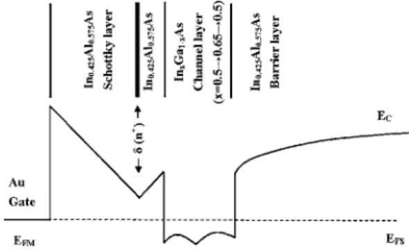
The epitaxial structure of the studied ␦-MHEMT was grown by the metal-organic chemical vapor deposition 共MOCVD兲 technique. Figure 1 shows the schematic conduction-band diagram and the layer structure of the stud- ied MHEMT. A 0.5-m-thick linearly graded InxAl1−xAs 共x
= 0→0.45兲 metamorphic buffer was deposited on the semi- insulating GaAs substrate. Upon the graded buffer, a 150-nm-thick undoped In0.425Al0.575As barrier layer, a 20 -nm-thick undoped InxGa1−xAs 共x=0.5→0.65→0.5兲 sym- metrically graded channel, a 5-nm-thick undoped In0.425Al0.575As spacer layer, a silicon planar doping layer, a 25-nm-thick undoped In0.425Al0.575As Schottky layer, a 2.5-nm-thick undoped InP recess-etch stopper, and finally a 20-nm Si-doped共1⫻1019cm−3兲 In0.5Ga0.5As cap layer were
a兲Author to whom correspondence should be addressed; electronic mail:
FIG. 1. Schematic conduction-band diagram of the studied MHEMT in equilibrium.
APPLIED PHYSICS LETTERS 88, 223506共2006兲
0003-6951/2006/88共22兲/223506/3/$23.00 88, 223506-1 © 2006 American Institute of Physics
Downloaded 13 Nov 2009 to 140.116.208.53. Redistribution subject to AIP license or copyright; see http://apl.aip.org/apl/copyright.jsp
grown, sequentially. The gate dimensions were 0.65⫻200m2with drain-to-gate spacing of 4m. The de- vice fabrication details and its room-temperature characteris- tics have been discussed in our previous work.5
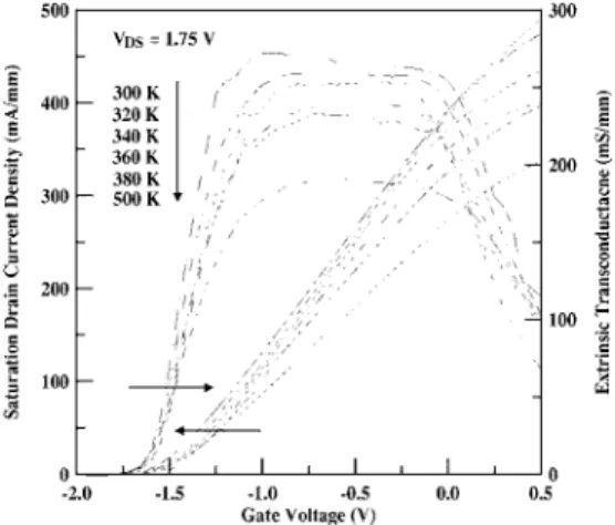
Figure 2 shows the common-source current-voltage characteristics of the studied device at different temperatures ranging from 300 to 500 K. The device demonstrates good pinch-off characteristics and superior output conductance characteristics due to the significant improvement on kink effects by using the symmetrically graded V-shaped InxGa1−xAs共x=0.5→0.65→0.5兲 channel. The device extrin- sic transconductance 共gm兲 and the saturation drain current density 共IDSS兲 as functions of the applied gate-source bias 共VGS兲 at elevated temperatures have been indicated in Fig. 3, with the drain-source voltage共VDS兲 fixed at 1.75 V. Defining IDSS0 to be the saturation drain current density at VGS= 0 V.
The IDSS0 共gm兲 values are 391 共271兲, 371 共254兲, 325 共231兲, 305 共215兲, 291 共203兲, and 273 共191兲 mA/mm 共mS/mm兲 at 300, 340, 380, 420, 460, and 500 K, respectively. Since the current density can be expressed by
J = qn2DEGv, 共1兲
where q is the carrier charge, n2DEG is the concentration of the two-dimensional electron gas共2DEG兲, and v is the aver- age carrier velocity. Though the background carrier concen- trations, increasing exponentially with temperature, increase the accumulative 2DEG concentration n2DEG within the
channel, the carrier transport velocityv is seriously degraded by the lattice scattering and carrier-carrier scattering mecha- nisms. Consequently, IDSS0decreases with the elevated tem- peratures. In addition, the characteristics of the extrinsic transconductance can be described11by
gm= gm0
1 + RS/gm0, 共2兲
where RSis the source series resistance, including the Ohmic contact resistance of the source/drain electrodes and the channel resistance within the gate-source region, and gm0 is the device intrinsic transconductance given12 by
gm0= v
dd+⌬d. 共3兲
is the permittivity of the Schottky layer, v is the average electron velocity in the channel, and共dd+⌬d兲 is the effective distance between the gate and the n2DEGlocation. Similar to the discussion for the IDSS0 dependences, the average elec- tron velocity will decrease with temperature due to the en- hanced scattering phenomenon. Therefore, with the fixed spacing between the gate and the n2DEGlocation, both of the intrinsic transconductance and the channel resistance will de- crease with temperature. Moreover, since the increase of the electrode contact resistance with temperature has also been verified in a previous report,11the above-mentioned combi- nation effects have resulted in the observed increase of the extrinsic transconductance characteristics with elevated tem- peratures.
The temperature dependences of the device threshold voltage, Vth共T兲 are shown in Fig. 4, with VDS= 1.75 V. The Vth values are −1.68, −1.641, −1.559, −1.572, −1.604, and
−1.84 V at 300, 340, 380, 420, 460, and 500 K, respectively.
Different temperature dependences have been observed as compared to the monotonous decreases of the threshold volt- age with temperature of the conventional GaAs-based het- erostructure field-effect transistors共HFETs兲.13,14The thresh- old shift共⌬Vth兲 from 300 to 420 K is only 0.108 V, and the calculated Vth/T value is 0.9 mV/ K. The observed posi- tive thermal threshold coefficient may be attributed to the following two mechanisms:
共1兲 Scattering phenomenon. The dominant lattice scattering and carrier-carrier scattering mechanisms15at high tem- peratures will significantly degrade the transport proper-
FIG. 2. Current-voltage characteristics from 300 to 500 K.
FIG. 3. Extrinsic transconductance and drain-source saturation current den- sity as a function of temperature.
FIG. 4. Temperature-dependent threshold characteristics and the linearity of gate-voltage swing of the studied MHEMT.
223506-2 Lee et al. Appl. Phys. Lett. 88, 223506共2006兲
Downloaded 13 Nov 2009 to 140.116.208.53. Redistribution subject to AIP license or copyright; see http://apl.aip.org/apl/copyright.jsp
ties, resulting in the decrease of both the average elec- tron velocity and the drain current, as described in Eq.
共1兲. Therefore, less magnitude of the reverse gate bias is required to deplete the channel.
共2兲 Enhanced channel confinement capability. As shown in Fig. 1, the devised high conduction-band discontinuity formed by the V-shaped InxGa1−xAs channel, together with the wide-gap and high-resistivity undoped In0.425Al0.575As spacer/buffer, can significantly improve the channel confinement capability, thus greatly reduc- ing the electron injection into the buffer.
Therefore, the above combinational effects have resulted in the observed positive thermal threshold coefficient for tem- peratures from 300 to 420 K in the proposed MHEMT.
On the other hand, the threshold voltage shift is −0.06 V from 420 to 500 K, as shown in Fig. 4, and the thermal threshold coefficient becomes negative at −0.75 mV/ K. An interesting polarity change of the thermal threshold coeffi- cient has resulted in the observed hump around 420 K. Since the threshold voltage of a ␦-doped HEMT can be approximated16by
Vth=⌽B
q −⌬EC
q −n2DEG共dd+⌬d兲
共5兲
by solving the one-dimensional Poisson equation without considering the applied drain-source transverse electric field.
⌽B is the Schottky gate barrier height, and ⌬EC is the conduction-band discontinuity between the Schottky layer and the InxGa1−xAs channel. As the ambient temperature reaches higher temperatures, the electrons in the substrate, after gaining enough thermal energy, start to surpass the channel/buffer discontinuity into the channel. The drain- source transverse field will further assist in this electron ther- mionic emission over the conduction-band discontinuity through the drain-induced barrier lowering17–19 共DIBL兲 mechanism. Moreover, in addition to the exaggerated sub- strate leakages, the increase of the intrinsic carrier concen- tration共ni兲 with temperature will also contribute to the sig- nificant increase of the channel carrier concentration n2DEGin Eq.共5兲, thus leading to the decrease of the threshold voltages at high temperatures. The variation of the thermal threshold coefficient of the proposed MHEMT is different from the monotonous decrease phenomenon.13,14This coefficient po- larity change may provide means to minimize the difference of the threshold voltage at high temperatures from its room- temperature operation.
Figure 4 shows the gate-voltage swing 共GVS兲 depen- dence on the ambient temperature by defining GVS as the corresponding bias range of VGSwith gmvalues no less than 90% of its peak characteristics 共gm,max兲. As compared to other high-temperature studies of the HFETs,13,14superiorly wide GVS of 1.13 V, with only 13% reduction from its room-temperature performance共1.3 V兲, can be still achieved at temperature up to 500 K. It is mainly due to the design of the symmetrically graded V-shaped channel of the present MHEMT. As described in Eq.共3兲, the effective spacing 共dd
+⌬d兲 will increase, while the 2DEG population is pushed away towards the channel/buffer side with the decreased gate bias. Nevertheless, since the electron saturation velocity in- creases with the In composition of the devised linearly graded InxGa1−xAs channel, the extrinsic transconductance
will thus be maintained with the decreased gate bias. Addi- tionally, with the designed high-barrier InxGa1−xAs/ InAlAs discontinuities to improve the 2DEG confinement capability, the present MHEMT demonstrates superior high-temperature GVS linearity. The device operated at 500 K also demon- strates comprehensively superior characteristics, including gm,max of 191 mS/ mm, IDSS0 of 273 mA/ mm, gate-drain breakdown voltage共BVGD兲 of −8.35 V, and forward turn-on voltage 共Von兲 of 0.959 V, with threshold variation of only 2.8%.
In summary, the present symmetrically graded ␦-doped InAlAs/ InxGa1−xAs/ GaAs MHEMT, with the enhanced channel carrier confinement capability, has exhibited an in- teresting polarity change of the thermal threshold coefficient at around 420 K. It is attributed to the switching of the domi- nant mechanisms between the carrier scattering within the channel and the thermionic emission over the conduction- band discontinuity within the channel/buffer heterointerface.
The device also demonstrated superior high-temperature GVS linearity, device gain, current drive, and breakdown characteristics at temperatures up to 500 K. Moreover, this work provides promising means to stabilize the device threshold by meticulously designing the variation control be- tween the thermal modulation effects, which is essential for the high-temperature MMIC applications.
This work was sponsored by the National Science Coun- cil of Taiwan, Republic of China under Contract No. NSC 94-2215-E-035-012.
1P. M. Smith, Conference Proceedings of the Seventh International Confer- ence on Indium Phosphide and Related Materials Conference, Sapporo, Japan共IEEE, New York, 1995兲, pp. 68–72.
2I. Watanabe, K. Shinohara, T. Kitada, S. Shimomura, Y. Yamashita, A.
Endoh, T. Mimura, T. Matsui, and S. Hiyamizu, IEEE Electron Device Lett. 26, 425共2005兲.
3L. Samoska, A. Peralta, M. Hu, M. Micovic, and A. Schmitz, IEEE Mi- crow. Wirel. Compon. Lett. 14, 56共2004兲.
4A. M. Kusters, A. Kohl, R. Muller, V. Sommer, and K. Heime, IEEE Electron Device Lett. 14, 36共1993兲.
5W. C. Hsu, Y. J. Chen, C. S. Lee, T. B. Wang, J. C. Huang, D. H. Huang, K. H. Su, Y. S. Lin, and C. L. Wu, IEEE Trans. Electron Devices 52, 1079 共2005兲.
6Y. J. Chen, W. C. Hsu, C. S. Lee, T. B. Wang, C. H. Tseng, J. C. Huang, D. H. Huang, and C. L. Wu, Appl. Phys. Lett. 85, 5087共2004兲.
7Y. J. Chen, C. S. Lee, T. B. Wang, W. C. Hsu, Y. W. Chen, K. H. Su, and C. L. Wu, Jpn. J. Appl. Phys., Part 1 44, 903共2005兲.
8K. Hosoya, K. Ohata, M. Funabashi, T. Inoue, and M. Kuzuhara, IEEE Trans. Microwave Theory Tech. 51, 2250共2003兲.
9M. Schallner and W. Konrath, IEEE MTT-S Int. Microwave Symp. Dig. 3, 2179共2001兲.
10G. Meneghesso, D. Buttari, E. Perin, C. Canali, and E. Zanoni, Tech.
Dig. - Int. Electron Devices Meet. 1998, 227.
11S. A. Hanka, C. H. Chen, P. Vold, and T. Akinwande, IEEE Trans. Reliab.
39, 571共1990兲.
12S. M. Sze, High-Speed Semiconductor Devices共Wiley-Interscience, New York, 1990兲, p. 302.
13W. C. Liu, K. H. Yu, R. C. Liu, K. W. Lin, K. P. Lin, C. H. Yen, C. C.
Cheng, and K. B. Thei, IEEE Trans. Electron Devices 48, 2677共2001兲.
14W. C. Liu, K. H. Yu, K. W. Lin, J. H. Tsai, C. Z. Wu, K. P. Lin, and C. H.
Yen, IEEE Trans. Electron Devices 48, 1522共2001兲.
15K. J. Chen, T. Enoki, K. Maezawa, K. Arai, and M. Yamamoto, IEEE Trans. Electron Devices 43, 252共1996兲.
16A. Mahajan, M. Arafa, P. Fay, C. Caneau, and I. Aesida, IEEE Trans.
Electron Devices 45, 2422共1998兲.
17C. S. Lee and W. C. Hsu, Appl. Phys. Lett. 84, 3618共2004兲.
18C. S. Lee, W. C. Hsu, and C. L. Wu, Jpn. J. Appl. Phys., Part 1 41, 5919 共2002兲.
19W. Fikry, G. Ghibaudo, and M. Dutoit, Electron. Lett. 30, 911共1994兲.
223506-3 Lee et al. Appl. Phys. Lett. 88, 223506共2006兲
Downloaded 13 Nov 2009 to 140.116.208.53. Redistribution subject to AIP license or copyright; see http://apl.aip.org/apl/copyright.jsp