行政院國家科學委員會專題研究計畫 期中進度報告
N 型及 P 型氧化鋅奈米柱之成長鑑定與相關奈米元件之製作
(2/3)
計畫類別: 個別型計畫 計畫編號: NSC94-2214-E-006-005- 執行期間: 94 年 08 月 01 日至 95 年 07 月 31 日 執行單位: 國立成功大學化學工程學系(所) 計畫主持人: 吳季珍 計畫參與人員: 黃鯤鵬 陳冠仁 古鎮豪 報告類型: 精簡報告 報告附件: 出席國際會議研究心得報告及發表論文 處理方式: 本計畫可公開查詢中 華 民 國 95 年 5 月 30 日
Abstract
The electric properties of the well-aligned ZnO nanorods grown on p-Si substrate under various molar ratios of Zn to O sources (MR) were investigated using the AC impedance analysis. Indium contacts were deposited on the ZnO nanorod surfaces and p++-Si backside to form the ohmic contacts. The device is suggested to be composed of p++-Si/n-ZnO nanorod junctions in parallel with air variable resistances. The carrier concentration of the ZnO nanorods is obtained from the slope of the linear relationship of the inverse capacitance squared and the reverse-biased voltage. The mobility is further calculated using the carrier concentration and the resistance of the ZnO nanorods extracted from the fitting results of the impedance data. The ZnO nanorods grown at the MRs of 6 x 10⁻⁴~1.3 x10⁻³ possess the carrier concentrations in the range of 1 x 10¹⁷~ 3 x 1018 cm3. The carrier concentration and the mobility of the ZnO nanorods increase with MR. In addition, the intensity decrease of the uv emission peak is observed in the photoluminescence spectra of the ZnO nanorods when the MR is increased. It is suggested that the decrease of the uv-emission intensity is ascribed to the increment of the carrier concentration of the ZnO nanorods.
One-dimensional (1D) semiconductor nanostructures have simulated considerable research efforts owing to their contributions to the understanding of fundamental concepts and their promising applications in nanoscale devices.[1] Determination of the electrical properties of the 1D semiconductor nanostructures is important for process and material developments as well as for further device design. Electrical properties of thin-film semiconductor materials, such as doping concentration and mobility, are usually measured with Hall effect measurements.[2] In the case of semiconductor nanowires, special test structures of the Hall effect measurement are difficult to be applied to the 1D nanostructures. Gate-dependent electrical transport measurements have been popularly employed to investigate the electrical transport properties of the semiconductor nanowires.[3] To perform such measurement, single nanowire field-effect transistors (FETs) have to be fabricated via the following procedure. Nanowires are collected from the substrates and dispersed on a SiO2 coated degeneratively doped Si substrate which acts as the back-gate in the
FET configuration. The source and drain electrodes are defined by electron beam lithography afterwards.[3] The mobility and carrier concentration of the nanowire can be estimated from transconductance measurements (source-drain current vs. gate voltage). The gate-dependent electrical transport measurement is time-consumed in fabricating the single nanowire FET although a lot of works for measuring electric properties of the single 1D nanostructures have been demonstrated using thise approach.[3] A more effective method to determine the electric properties of the nanowires is needed for the nanodevices which are dispensable manufactured “nanowire by nanowire”.
capacitance-voltage (C-V) measurement is an alternative method to determine the doping concentrations in semiconductors.[2,4] Schottky and pn junctions with one side of the junction being much more heavily doped than the other side are employed for C-V analysis. A fixed dc reverse bias superimposing a small ac voltage is applied on the sample for measuring the depletion capacitance of the junction at a fixed frequency. The inverse capacitance squared is linear function of applied reverse-biased voltage and the built-in potential as well as the carrier concentration of the lightly doped side can be estimated from the intercept and the slope. This Mott-Schottky approach is also performed when a Schottky barrier is formed at the interface of the semiconductor film and electrolyte to monitor the carrier concentrations in the film.[5] C-V characteristics of the nonideal samples, which can not be analyzed by standard C-V measurement, have also been investigated by analyzing the frequency dependent impedances Z of the samples.[6] Elements, such as capacitances and resistances, can be extracted from an equivalent circuit of the reverse-biased sample obtained by curve fitting. The linear relationship of the inverse capacitance squared and the reverse-biased voltage can be thus established to estimate the carrier concentration in the semiconducting materials.
To develop a simple method other than the gate-dependent electrical transport measurement for investigating the electric properties of the 1D semiconductor nanostructures, herein we report on the determination of the carrier concentrations and the mobility of the well-aligned ZnO nanorods on Si substrates using AC impedance analysis. To form a p++-n junction for impedance analysis, well-aligned ZnO nanorods were grown on degenerate p-type Si substrates (with a hole concentration ~ 1020 cm-3) via a catalytic-free MOCVD method.[7] The frequency dependences of the impedances of the samples under various reverse biases were measured. An
equivalent circuit model considering the special feature of the sample was established to represent the measured data and was employed to extract the space-charge capacitances and the resistances in the ZnO nanorods for the determination of the carrier concentrations and the mobility. The electric properties of the ZnO nanorods grown under various conditions were investigated using the AC impedance analysis.
Well-aligned ZnO nanorods were grown on p++-Si substrates in a two-temperature-zone furnace. The detailed experimental setup and procedure for ZnO nanorod growth have been described elsewhere.[7] In brief, zinc acetylacetonate (Zn(C5H7O2)2), which was employed to be zinc source, placed on a
cleaned Pyrex glass container was loaded into the low temperature zone of the furnace. The temperature was controlled to be at 120-130oC to vaporize the solid reactant. The vapor was carried by a N2/O2 flow into the high temperature zone of the furnace
in which substrates were located. The substrate temperature and the total pressure were 590oC and 200 Torr, respectively, during ZnO nanorods growth. In the present work, the carrier concentrations and the mobility of the ZnO nanorods grown on the p++-Si substrates at various molar ratios of the zinc to oxygen sources, MR, were
investigated using AC impedance analysis. Figure 1 shows typical SEM images of the ZnO nanorods deposited on the p++-Si substrate. To perform the impedance analysis of the p++-Si/n-ZnO nanorod junctions, as show in Figure 2 (a), the indium contacts were deposited on the ZnO nanorod surfaces and Si backside to form the ohmic contacts. Figure 2(b) shows that a thin indium film is formed continuously on the ZnO nanorod surfaces, revealing that the device is composed of p++-Si/n-ZnO nanorod junctions in parallel with air constant phase elements (CPE), CPEair. AC
impedance measurements were carried out by applying a 10 mV ac signal over the frequency range of 10-106 Hz on the top of the revise-biased voltages using a
potentiostat with a frequency response analyzer (PGSTAT30 and FRA2 module, Autolab). The suggested ideal equivalent circuit of the device is illustrated in Figure 2(c), where Rs, RZnO, RSC and CPESC are the series resistance of contacts and outer
circus, the resistance of the ZnO nanorods and the resistance and the constant phase element (capacitance) of the space-charge region at the p++-Si/n-ZnO nanorod junctions, respectively.
Figure 1 Typical SEM images of the ZnO nanorods deposited on the p++-Si substrate. (a) top view and (b) cross-sectional view.
Figure 2 (a) A scheme of the device of the p++-Si/n-ZnO nanorod junctions. (b) SEM image of the ZnO nanorods covered with an In thin film. (c) The suggested ideal equivalent circuit of the device in (a).
Typical I-V curve of the devices is shown in Figure 3(a). The ZnO nanorods were grown on the p++-Si substrate at a MR of 7.6 x 10⁻⁴. In contrast to the I-V characteristic curve of an ideal p-n junction, the inset of Figure 3(a) reveals that the current increases slightly with the reverse bias. Figure 3(b) shows the Nyquist plots
(a) (b) (c)
(b) (a)
of the impedance data of the device under various applied reverse-bias voltages. The total resistance of the device decreases when the reserve-bias voltage is increased, which is inconsistent with the tendency predicted according to the equivalent circuit model in Figure 2(c). On the other hand, the resistances under reverse bias conditions estimated using
0 < =V V dI dV
from Figure 3(a) are consistent with the total resistances of the RC components shown in Figure 3(b). Due to the humidity and the poor strength of the free-standing In metal electrode in the air region, we suggested that the decreased total resistance may be ascribed to the breakdown of the CPEair under the reverse bias conditions. The CPEair is thus replaced by a variable
resistance, Rair, as shown in the equivalent circuit of Figure 3(c). The theoretically
expected behavior of the impedance Z of the equivalent circuit of Figure 3(c) is
) ( ) ( ] ) ( [ ) ( sc air n sc sc ZnO sc air n sc ZnO sc ZnO sc air s R R CPE j R R R R CPE j R R R R R R Z + + + + + + + = ω ω ω (1) 2 2 2 2 2 2 2 2 2 2 2 2 ) ( ) ( ) ( ] [ ) ( ) ( 2 ) ( ) Re( air ZnO sc sc sc ZnO air ZnO sc air ZnO sc air sc sc ZnO air sc ZnO air ZnO sc air R R CPE R R R R R R R R R R CPE R R R R R R R R R Rs Z n n + + + + + + + + + + + = ω ω (2) 2 2 2 2 2 ) ( ) ( ) ( ) ( ) ( 2 air ZnO n sc sc sc ZnO air n sc sc air R R CPE R R R R CPE j R R Z lm + + + + − = ω ω (3)
where ω is the angular frequency of the ac signal. The fitting curves according to the revised equivalent circuit are also illustrated in Figure 3(b). In comparison with the measured impedance data, they reveal the realization of the equivalent circuit model shown in Figure 3(c). The elements extracted from the equivalent circuit are listed in Table I.
Figure 3 (a) Typical I-V curve of the devices. (b) The Nyquist plots and their fitting curves of the impedance data of the device under various reverse-bias voltages. (c) The equivalent circuit of the device.
Table I The elements extracted from the equivalent circuit in Figure 3(b).
V(V) Rs(Ω) RZnO(mΩ) RSC(MΩ) CPESC(nF) p Rair(kΩ)
0.05 9.76 0.556 0.681 78.8 0.97 2.7 0.1 9.81 0.556 0.681 76.6 0.969 2.58 0.15 9.86 0.556 0.681 74.7 0.97 2.44 0.2 9.87 0.556 0.681 72.7 0.969 2.3 0.25 9.88 0.556 0.681 70.8 0.969 2.19 0.3 9.89 0.556 0.681 68.9 0.968 2.09 0.35 9.90 0.556 0.681 67 0.969 2 0.4 9.92 0.556 0.681 65.1 0.967 1.93
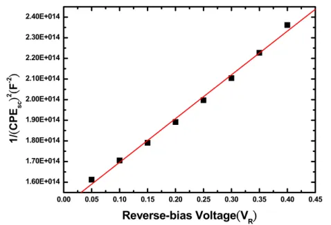
Figure 4 shows the plot of 1/( )2
SC
CPE vs VR of the p++-Si/n-ZnO nanorod junctions in which the CPESC are extracted from the fitting curves shown in Table I and VR are the dc voltages across the space-charge region under various applied reverse bias.[4] In the case of heterojunction, the relationship between the space-charge region capacitance and the doping concentrations of the semiconductors is[2]
(
)
(
)
R bi p n ap dn ap p dn n SC V V A N qN N N CPE + + = 2 2 2 ) ( 1 ε ε ε ε (4)where q is the elementary charge, N and N are the carrier concentrations of the
(c) -0.5 0.0 0.5 1.0 1.5 2.0 0.00 0.01 0.02 0.03 0.04 0.05 0.06 Curr en t( A) Voltage(V) (a) -0.5 -0.4-0.3 -0.2 -0.10.0 0.1 0.2 0.3 0.4 0.5 -0.0010 -0.0005 0.0000 0.0005 0.0010 Cu rr en t(A) Voltage(V) (b)
n- and p-type semiconductors, εn and εp are the permittivities of the n- and p-type semiconductors, A is the area of the diode and V is the built-in potential. In this bi
study, N , the acceptor concentration of the pap ++-Si substrate was determined by Hall effect measurement to be 1.1 x 1020 cm-3. Therefore, the carrier concentration of the ZnO nanorods N and the built-in potential dn V can be estimated from the slope bi
and the intercept of 1/( )2
SC
CPE vs VR, respectively. The total space-charge region width W under reverse bias can be expressed as following:[2]
(
)
(
)
(
)
(
)
2 / 1 2 2 / 1 ) ( 2 ) ( 2 ) ( 2 ⎪⎭ ⎪ ⎬ ⎫ ⎪⎩ ⎪ ⎨ ⎧ + + + = ⎪⎭ ⎪ ⎬ ⎫ ⎪⎩ ⎪ ⎨ ⎧ + + + + + = + = ap p dn n ap dn R bi ap dn p n ap p dn n ap R bi dn p n ap p dn n dn R bi ap p n p n N N N eN V V N N N N eN V V N N N eN V V N x x W ε ε ε ε ε ε ε ε ε ε ε ε (4)where x and n x are the space-charge widths in the n and p regions of the pn p
junction, respectively. Table II shows the N and the dn V estimated from Figure 4 bi
and eq. (3) as well as x , n x and W under various Vp R calculated from eq. (4). Figure 5 shows the ideal energy-band diagram of the p++-Si/n-ZnO nanorods heterojunctions in thermal equilibrium. Moreover, the mobility of the ZnO nanorods is further estimated using the following relation:[2]
dn
nN
qμ
σ = (5) where σ and μn are the conductivity and the electron mobility of the ZnO nanorods. RZnO listed in Table I which was obtained from the curve fitting of the
Nyquist plots of the device is employed to calculate the conductivity. The electron mobility of the ZnO nanorods grown at a MR of 7.6 x 10⁻⁴ is estimated to be 4.7 cm2/V-s.
Figure 4 Plot of 1/( )2
SC
CPE vs VR of the p++-Si/n-ZnO nanorod junctions.
Table II N and dn μn of the ZnO nanorods grown at a MR of 7.6 x 10⁻⁴. V and bi n
x , x as well as W of the pp ++Si/ZnO nanorod junctions under various V
R. Ndn (cm-3) μn(cm 2/V-s) Vbi (eV) A (cm2) 5.5 x 10¹⁷ 4.7 0.7 0.365 VR(V) Xn(nm) Xp(nm) W(nm) 0.05 34.6 0.2 34.8 0.1 35.7 0.2 35.9 0.15 36.8 0.2 37.0 0.2 38 0.2 38.2 0.25 39 0.2 39.2 0.3 40 0.2 40.2 0.35 41 0.2 41.2 0.4 42 0.2 42.2 0.00 0.05 0.10 0.15 0.20 0.25 0.30 0.35 0.40 0.45 1.60E+014 1.70E+014 1.80E+014 1.90E+014 2.00E+014 2.10E+014 2.20E+014 2.30E+014 2.40E+014 1/ ( CP E sc ) 2 (F -2 ) Reverse-bias Voltage(VR)
Figure 5 Ideal energy-band diagram of p++-Si/n-ZnO nanorods heterojunctions in thermal equilibrium.
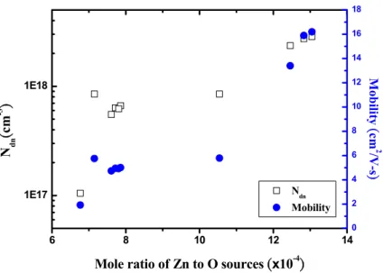
Figure 6 shows the influence of the molar ratio of the Zn to O sources on the carrier concentrations and the electron mobility of the ZnO nanorods. It reveals that the ZnO nanorods grown at the MRs of 6 x 10⁻⁴~1.3 x10⁻³ possess the carrier
concentrations in the range of 1 x 10¹⁷~ 3 x 1018 cm3. The carrier concentration and the mobility of the ZnO nanorods increase with MR. The nanorods with the carrier concentrations of ~1017 cm3 exhibit the mobility in the range of 2-6 cm2/V-s whereas those with carrier concentrations of 1-3 x 1018 cm3 possess the mobility of 13-17 cm2/V-s. The room-temperature photoluminescence (PL) spectra of the ZnO
nanorods grown at various MRs are shown in Figure 7. The lengths, diameters and densities of the ZnO nanorods shown in the Figure are almost the same. Figure 7 demonstrates the uv emission peaks at 378 nm and the absence of the green band emission in these PL spectra. The intensity of the uv emission peak decreases when the MR is increased. In comparison with the carrier concentration dependence of the MR, it is suggested that the decrease of the uv-emission intensity is ascribed to the increment of the carrier concentration of the ZnO nanorods.
Figure 6 Influence of molar ratio of Zn to O sources on carrier concentrations and electron mobility of the ZnO nanorods.
Figure 7 PL spectra of the ZnO nanorods grown at various MRs.
Summary
Determination of the electric properties of the 1D nanostructures using Ac impedance analysis has been developed in the present work. The carrier concentration and electron mobility of the well-aligned ZnO nanorods grown on p-Si substrate at various molar ratios of Zn to O sources (MR) were investigated using the AC impedance analysis. Indium contacts were deposited on the ZnO nanorod
6 8 10 12 14
1E17 1E18
Ndn Mobility
Mole ratio of Zn to O sources (x10-4)
N dn ( cm -3 ) 0 2 4 6 8 10 12 14 16 18 Mobili ty ( cm 2 /V-s ) 350 400 450 500 550 600 0 500 1000 1500 2000 2500 3000 In tensi ty Wavelength(nm) MR = 6.8 x10⁻⁴ MR = 10.5 x10⁻⁴ MR = 12.8 x10⁻⁴
surfaces and p++-Si backside to form the ohmic contacts. The device is suggested to be composed of p++-Si/n-ZnO nanorod junctions in parallel with air variable resistances. The carrier concentration of the ZnO nanorods is estimated from the slope of the linear relationship of the inverse capacitance squared and the reverse-biased voltage. The mobility is further calculated using the carrier concentration and the resistance of the ZnO nanorods extracted from the fitting results of the impedance data. The ZnO nanorods grown at the MRs of 6 x 10⁻⁴~1.3 x10⁻³ possess the carrier concentrations in the range of 1 x 10¹⁷~ 3 x 1018 cm3. The carrier
concentration and the mobility of the ZnO nanorods increase with MR. In addition, the intensity decrease of the uv emission peak is observed in the photoluminescence spectra of the ZnO nanorods when the MR is increased. It is suggested that the decrease of the uv-emission intensity is ascribed to the increment of the carrier concentration of the ZnO nanorods.
References
[1] (a) Lieber, C. M. Solid State Commun. 1998, 107, 607-616. (b) Hu, J.; Odom, T. W.; Liber, C. M. Acc. Chem. Res. 1999, 32, 435-445.
[2] Neamen, D. A. Semiconductor Physics and Devices, 2003, 3rd ed., McGraw-Hill: New York.
[3] (a) Cui, Y.; Duan, X.; Hu, J.; Lieber, C. M. J. Phys. Chem. B 2000, 104, 5213-5216. (b) Huang, Y.; Duan, X.; Cui, Y; Lieber, C. M. Nano Lett. 2001, 2, 101-104. (c) Goldberger J.; Sirbuly, D. J.; Law. M.; Yang. P. J. Phys. Chem. B
2005, 109, 9-14.
[4] (a) Friesen, G.; Dunlop, E. D.; Wendt, R. Thin Solid Films 2001, 387, 239-242. (b) Chaure, N. B.; Bordas, S.; Samantilleke, A. P.; Chaure, S. N.; Haigh, J.; Dharmadasa, I. M. Thin Solid Films 2003, 437, 10-17.
[5] (a) Windisch Jr., C. F.; Exarhos, G. J. J. Vac. Sci. Technol A 2000, 18, 1677-1680. (b) Chemla, M.; Bertagna, V.; Erre, R.; Rouelle, F.; Petitdidier, S.; Levy, D.
Electrochem. Solid-State Lett. 2003, 6, G7-G11.
[6] (a) Straub, A.; Gebs, R.; Habenicht, H.; Trunk, S.; Bardos, R. A.; Sproul, A. B.; Aberle, A. G. J. Appl. Phys. 2005, 97, 083703. (b) Meier, M.; Karg, S.; Riess, J.
Appl. Phys. 1997, 82, 1961-1966. (c) Meijer, E. J.; Mangnus, A. V. G.; Hart, C.
M.; de Leeuw, D. M.; Klapwijk, T. M. Appl. Phys. Lett. 2001, 78, 3902-2904. [7] (a) Wu, J.-J.; Liu, S.-C. Adv. Mater. 2002, 14, 215-218. (b) Wu, J.-J.; Liu, S.-C. J.