行政院國家科學委員會專題研究計畫 成果報告
以低溫共燒陶瓷技術研製車用防撞感測系統之射頻關鍵模 組--總計畫:以低溫共燒陶瓷技術研製車用防撞感測系統之
射頻關鍵模組 研究成果報告(精簡版)
計 畫 類 別 : 整合型
計 畫 編 號 : NSC 96-2221-E-011-005-
執 行 期 間 : 96 年 08 月 01 日至 97 年 07 月 31 日 執 行 單 位 : 國立臺灣科技大學電機工程系
計 畫 主 持 人 : 楊成發
共 同 主 持 人 : 林舜天、馬自莊、廖文照、曾昭雄 計畫參與人員: 博士班研究生-兼任助理人員:劉獻文
處 理 方 式 : 本計畫涉及專利或其他智慧財產權,2 年後可公開查詢
中 華 民 國 97 年 10 月 31 日
以低溫共燒陶瓷技術研製車用防撞感測系統之射頻關鍵模組-
總計畫:以低溫共燒陶瓷技術研製車用防撞感測系統之射頻關鍵模組
計畫編號:NSC 96-2221-E-011-005
執行期限:96 年 08 月 01 日至 97 年 07 月 31 日 計畫主持人:楊成發 教授 國立台灣科技大學 電機工程系 計畫共同主持人:馬自莊 教授、廖文照 教授、曾昭雄 教授
摘 要
本整合型研究計畫為期一年,以研製車用防撞預 警感測系統之射頻關鍵模組。本計畫包含四個子計 畫,其結合射頻、天線與微波電路等各領域之最新技 術,來進行高安全性、高靈敏性、高精確性之智慧車 用防撞預警系統射頻關鍵模組之研發,以提升車用電 子技術之應用層面,具學術研究之前瞻性與新穎性。
該車用防撞預警感測系統涵蓋天線、主被動射頻電 路、電磁脈衝技術、電磁相容及雷達射頻模組等研究 範圍。子計畫一負責微型化濾波器及低雜訊放大器之 研發,子計畫三負責車用無線感測節點之微型化超寬 頻射頻模組之研發,子計畫四負責微型晶片天線研發 及車內外電波傳播、電磁相容特性分析及評估,而子 計畫五則專注於微型化雷達射頻模組之研製與微波介 質量測技術之建立。透過本整合型計畫之執行,將能 為國內無線通訊業界培育射頻、天線及微波電路等相 關領域之人才,具產業價值與技術前瞻性。
關鍵詞:汽車防撞預警、晶片天線、微波濾波器、微 波放大器、超寬頻電磁脈衝技術、無線感測節點、電 波傳播、電磁相容、射頻雷達模組、微波量測技術
子計畫一:
微型化放大器與濾波器射頻模組之研製
主持人:楊成發 教授(台灣科技大學電機工程系)
進行步驟及預期完成之工作項目如下:
1. 依據元件特性及電路規劃,擬訂系統規格。
2. 研製平面式微型化共振器與窄頻帶通濾波器。
3. 研製平面式微型化寬頻轉接電路及帶通濾波器。
4. 研製平面式微型化轉接電路。
5. 研製平面式低雜訊放大器。
6. 量測平面式濾波器、放大器與轉接電路之特性。
子計畫三:
超寬頻無線感測節點之微型化射頻前端電路研製 主持人:馬自莊 副教授(台灣科技大學電機工程系)
進行步驟及預期完成之工作項目如下:
1. 依據元件特性及電路規劃,擬定系統規格。
2. 完成平面人造傳輸線及平面可電氣控制轉接之效 能改良。
3. 完成超寬頻射頻模組之平面電路設計與系統整合 測試。
4. 完成多層人造傳輸線之模擬研究及初步測試,並提 供子計畫一必要之技術支援。
子計畫四:
車用微型晶片天線與電磁傳播環境特性研究
主持人:廖文照 教授(台灣科技大學電機工程系)
進行步驟及預期完成之工作項目如下:
1. 擬訂車用預警防撞雷達天線傳輸規格。
2. 研製平面式高增益微帶陣列天線,供原型車用雷達 使用,並與子計畫一、五之射頻電路及雷達模組整 合。
3. 研製平面式超寬頻天線,供 UWB 無線傳輸模組使 用,並與子計畫一、三之射頻電路及UWB 前端模 組整合。
4. 使用高頻電磁方法,建立車輛模型,評估 UWB 天 線傳輸效能。
子計畫五:
微型化雷達射頻模組研製⎯使用微波六埠網路 主持人:曾昭雄 教授(台灣科技大學電子工程系)
進行步驟及預期完成之工作項目如下:
1. 系統規劃及模擬,並擬定元件規格。
2. 研製平面結構之六埠網路及方向耦合器,並完成相 關效能測試。
3. 使用市售之壓控振盪器、除頻器、相位檢測及鎖相 迴路IC 組裝具有鎖相迴路之射頻訊號源電路,並 進行電路特性量測。
4. 撰寫「類比/數位資料擷取」及「數位/類比控制輸 出」等儀控程式。
5. 使用介質合成波導及 LRR 校準技術開發新式寬頻 材料量測技術。
計畫編號:NSC 96–2221–E–011–086 執行期限:96 年 08 月 01 日至 97 年 07 月 31 日 計畫主持人:楊成發 教授 國立台灣科技大學 電機工程系 計畫參與人員:劉獻文、林郁書、陳炳志、吳國賢、蕭新朧
摘 要
智慧型車用電子系統近年來廣泛受到重視,其中 針對車用防撞感測系統之發展,開發具有低成本與高 穩定性之射頻關鍵零組件是相當重要的。另外,結合 汽車微控制器之應用以及裝置小型化之趨勢,車用防 撞感測系統之射頻模組也必須走向微型化。因此,本 子計畫擬研製車用防撞感測系統之射頻關鍵零組件,
其中包括:寬頻濾波器、窄頻濾波器與低雜訊放大器 等射頻元件,並與其他子計畫整合完成車用防撞感測 系統之射頻關鍵模組。計畫中將使用射頻電路模擬軟 體 ADS、電磁全波模擬軟體 XFDTD 與 HFSS 來進行 上述射頻關鍵零組件之分析與設計,並且實作平面式 濾波器、放大器及轉接電路,以與其他子計畫整合之。
關鍵詞:車用防撞感測系統、濾波器、放大器、射頻 前端模組
Abstract
Intelligent automotive electronic systems have attracted large attentions in recent years. Particularly, it is very important to develop RF key modules with a low cost and very stable performance for an automotive collision-avoidance sensing system. Besides, in order to combine the applications of automotive Micro Control Units (MCU) and device miniaturization, the RF modules of the automotive collision-avoidance sensing system need to be miniaturized. Thus, this sub-project will develop RF key components for the automotive collision-avoidance sensing system in three years, which include wideband filters, narrowband filters and low noise amplifiers (LNA). Therefore, these RF elements can be integrated with those from other sub-projects for realizing the RF key modules of the automotive collision-avoidance sensing system. The RF circuit simulator ADS, full-wave electromagnetic simulation software packages XFDTD and HFSS are employed to analyze and design the RF key components to integrate with other sub-projects.
Key words: Automotive collision-avoidance sensing system, Filter, Amplifier, RF front-end module
一、簡介
由於近幾年來全球各大車廠對於安全、舒適性與 環保方面不斷地提昇,讓車用微控制器(Micro Control Unit, MCU)與周邊電子系統的溝通連結也變得越來越 依靠無線通訊之 RF 相關電子技術,目前多方研究已 經逐步實現將車用電子技術[1][2]融入實用化的階段 了。針對寬頻濾波器、窄頻濾波器與低雜訊放大器等 射頻元件之相關技術發展,國內外已有許多文獻發 表,例如:平面式濾波器設計[3]-[8]、轉接電路[9]-[12]
與放大器模組[13]等。平面式濾波器具有高整合性及 低製造成本,一直是射頻電路系統中最常用的結構,
本子計畫擬應用微帶線和共平面波導兩種結構來開發 適合於窄頻與超寬頻段之共振器與轉接電路,並研製 應用於微波帶通濾波器,以提供給子計畫三之車內通 訊介面以及子計畫五之雷達收發模組之用。此外,本 子計畫研究重點亦包括放大器模組。一般說來,在射 頻訊號透過天線接收之後,會由一個前級低雜訊放大 器(Low Noise Amplifier, LNA)放大所接受到的訊號,
然後再以振盪器混波而輸出,其中包括射頻和中頻訊 號,並透過帶通濾波器得到中頻訊號,再進行後續處 理。在低雜訊放大器部分,將應用子計畫三所發展之 人工傳輸線(Artificial Transmission Line, ATL)技術來 設計低雜訊放大器,並且搭配子計畫四所研製之天線 元件,一起整合成射頻前端模組。
二、超寬頻帶通濾波器之設計與分析 本計畫所提出具截止頻帶之超寬頻帶通濾波器,
其主要的架構是由微帶線至共平面波導轉換器以背對 背之型式所組成,而此轉換器乃由三個主要元件所建 構而成:一段長度在頻率 5.75GHz 為四分之一波導波 長之短路殘段、開路微帶線及短路共平面波導。此具 有 截 止 頻 帶 特 性 之 濾 波 器 於 操 作 頻 段 3.1GHz- 10.6GHz 內具備良好的帶通頻率響應,並含有濾除無 線區域網路信號的頻帶截止功能,其電路架構如圖一 所示,其基板是採用 FR4 玻璃纖維板,其相對介電係 數為εr = 4.4、損耗正切為 tanδ = 0.02,而整體電路尺 寸為 30(L)×14(W)×0.4(H)mm3。如圖二所示,此帶通 濾波器應用了微帶線至共平面波導之轉接器,其利用 一段長度在中心頻率 6.85GHz 為四分之一波導波長之 開路微帶線,使其在中心頻率下可於 A 點產生虛接地 之效果,進而達到微帶線與共平面波導匹配的目的。
另一方面,在轉接器阻抗匹配方面,亦可透過選擇適 當的共平面波導特徵阻抗來加以實現之。由於欲將特 定頻帶之干擾雜訊予以濾除,故將一長度在特定頻率 5.75GHz 為四分之一波導波長之短路殘段加入至微帶
以低溫共燒陶瓷技術研製車用防撞感測系統之射頻關鍵模組-
子計畫一:微型化放大器與濾波器射頻模組之研製
線到共平面波導之轉接器中,使本濾波器附加具有截 止特定頻帶訊號之特性,進而達到超寬頻通訊系統對 於雜訊抑制的需求。
圖一 具有頻帶截止特性之超寬頻帶通濾波器
圖二 微帶線至共平面波導之轉接器
本計畫使用 HFSS 套裝軟體進行濾波器之電路設 計及參數模擬,並應用高效能向量網路分析儀來進行 效能驗證,其中濾波器之實作如圖三所示。由圖四的 頻率響應可以得知,此款具頻帶截止特性之超寬頻帶 通濾波器於操作頻段 3.1GHz-10.6GHz 中具有良好的 頻率響應,其傳輸損失於中心頻率 6.85GHz 為 1dB,
並在起始頻率 3.1GHz 與截止頻率 10.6GHz 分別為 0.58dB 與 2.42dB,而在截止頻段 5.75GHz 之傳輸損失 則為 12dB,其中實測與模擬之結果有些微差異,此可 能是因為製程上的誤差所導致。另外,由於本濾波器 所選用之基材為 FR4 玻璃纖維板,其材料特性會導致 濾波器之傳輸損失於高頻時的表現較為不理想。此 外,由於製程誤差的緣故,使得所量測之反射損失會 略差於模擬值。在群延遲量測方面,其頻率響應如圖 五所示,結果顯示:此款超寬頻帶通濾波器於通帶頻 段裡具有良好之群延遲響應,其變動介於 0.26ns 之 間,故寬頻信號可以從天線端經由本濾波器正確地傳 遞至接收機。
(a)正面 (b)背面 圖三 超寬頻帶通濾波器之實作
圖四 超寬頻帶通濾波器之傳輸與反射損失
圖五 群延遲頻率響應
吾人於設計此濾波器時,乃先針對四分之一波導 波長之短路殘段來進行模擬分析,其電路模擬架構如 圖六所示,而其工作原理為利用在特定頻率下為四分 之一波導波長之短路殘段來併入至一微帶線中,其輸 入能量經由微帶線透過電磁耦合之方式,會耦合至短 路殘段中,使短路殘段於特定頻段底下產生共振效 果。由圖七的傳輸及反射損失結果可以得知:四分之 一波導波長之短路殘段可有效導引出一特定截止頻 段,故運用此短路殘段與超寬頻帶通濾波器來加以結 合,使得濾波器可具有攔截特定頻帶訊號之特性,進 而應用至阻隔特定頻段之雜訊干擾。另外,於模擬的 過程當中,可先對短路殘段的共振結構進行設計。之 後,再針對超寬頻帶通濾波器進行模擬,其目的是為 了減少整體電路設計之運算時間。最後,當個別元件 之效能響應均達到預期目標時,再將其結合以進行整 體的電路模擬,此分析方法可有效提昇電路設計之效 率。為了詳細分析此短路殘段之共振特性,本計畫亦 研究模擬不同 Lstub長度之短路殘段,其傳輸損失之頻 率響應如圖八所示。由此圖可得知:藉由控制短路殘 段之長度,可有效地調整其共振頻率點,進而控制及 移動濾波器之截止頻帶,使得本超寬頻帶通濾波器具 有可控截止頻帶之特性而於設計上可加以靈活運用。
圖六 短路殘段之電路模擬架構
圖七 短路殘段之傳輸與反射損失模擬
圖八 不同長度之短路殘段特性
由圖九(a)和(c)之表面電流分佈可知:當操作頻率 為濾波器之帶通頻段時,其能量會從埠 1 端透過左側 的轉接器將能量從微帶線模態耦合至共平面波導模 態,並且藉由共平面波導將能量饋入至右側的轉接 器。其次,右側轉接器會將其所接收之能量轉換至微 帶線模態,並繼續傳導至埠 2 端。另外,由圖九(b)之 表面電流分佈亦可看出,當操作頻率在此濾波器之截 止頻帶 5.75GHz 時,其四分之一波導波長之短路殘 段會於該頻率產生共振效果,使埠 1 端之轉換器無法 順利地將能量從微帶線模態耦合進共平面波導模態,
致使能量無法繼續傳遞,故藉由此電路特性可達到阻 隔特定頻段訊號之目的。
(a)4GHz
(b) 5.7GHz
(c) 8GHz
圖九 表面電流密度分佈於 4GHz、5.7GHz 與 8GHz
三、窄頻濾波器之設計與分析
由於窄頻濾波器亦為汽車防撞模組的關鍵元件之 一 , 因 此 本 子 計 畫 另 以 步 階 阻 抗 共 振 器 (Stepped Impedance Resonator, SIR) 來設計濾波器,並且使用 RO4003低損耗板材來當作基板,其相對介電係數為εr
= 3.38、損耗正切為tanδ = 0.0027,而整體電路尺寸為 14(L)×12.5(W)×0.508(H)mm3,其濾波器電路結構如圖 十所示,而圖十一為實作成品。為了有效掌握濾波器 的共振特性,我們可根據下列的式子來設計SIR共振 器的尺寸,並進一步調整電路阻抗:
2 1
1
tan ( )
k
(1)2 1/ Z
Z
k
(2) 其中Z1、Z2分別為兩埠的特性阻抗,θ1、θ2為相對應之 電氣長度,而k為特性阻抗比。此外,為了有效縮減此 濾波器之電路總面積,吾人亦透過鑽孔(via hole)的方 式來達成,使得原先的共振長度從原本的λg/2變成 λg/4。其次,由於此SIR共振器會附帶產生一些高階諧 波(high-order harmonics),進而影響到濾波器的效能,故本濾波器的饋入結構乃設計成具有同振幅、相位相 差180度的傳輸結構,並可產生相對應之傳輸零點 (transmission zero),其中我們亦可以利用電路中的兩 個片形(patch)金屬來輔助抑制高階諧波。由圖十二中 可以得知,此濾波器於2.4GHz操作頻段內具備良好的 傳輸與反射損失,其能夠提供良好的濾波響應,而我 們亦可從S參數中看出吾人所設計的饋入結構可以有 效的抑制高階諧波產生,進而提升窄頻濾波器的整體 效能。此外,在高頻部份所產生的誤差乃是由於電路 製程差異與模擬參數未完整精準考量所致。
圖十 步階阻抗共振器實現窄頻濾波器
圖十一 窄頻濾波器實作
圖十二 窄頻濾波器之傳輸與反射損失
另一方面,本計畫亦提出另一款具有較佳傳輸零 點的窄頻濾波器,其設計原理也是基於SIR共振器,
且同樣採用RO4003低損耗板材,其整體電路尺寸為 24(L)×24(W)×0.508(H)mm3,其濾波器電路結構如圖 十三所示,而圖十四為實作電路。此濾波器的饋入結 構與前一款的設計方式雷同,其具有同振幅、相位相 差180度的傳輸結構。為了獲得更好的濾波效能,濾波 器的傳輸零點必須設計成更為陡峭以符合規格,因此 乃 利 用 交互 耦 合的 方 式來改 善 通 帶響 應 (pass-band response),其中耦合方式包含電場耦合與磁場耦合兩 種。在特定的頻率當中,上述兩種耦合方式會產生相 同振幅與180度相位差的響應,進而於通帶附近造成兩 個極為陡峭傳輸零點,使得濾波器的整體效能可以相 對提高。由圖十五中可以得知,此款濾波器於2.4GHz 通帶部份有兩個設計良好的傳輸零點,所以我們可以 獲得良好的傳輸與反射損失,進而能夠提供更好的濾 波響應。另外,在高頻部份所產生的誤差乃是由於電 路製程差異與模擬參數未完整精準考量所致,而共振 電路的Q值偏高,亦會使得模擬精準度受到一些影響。
圖十三 窄頻耦合濾波器
圖十四 窄頻耦合濾波器實作
圖十五 窄頻耦合濾波器之傳輸與反射損失
四、寬頻低雜訊放大器模組之設計與分析 為了配合子計畫四所設計之寬頻天線,本計畫亦 設計一款寬頻低雜訊放大器模組以增加汽車防撞系統 的信號解析能力,其整體模組的電路結構包含了兩個 多單元分支線段(multi-cell branch-line)和一個低雜訊 放大器。為降低傳輸損耗,我們乃採用RO4003低損耗 板材來作為製程基板,其放大器電路結構如圖十六所 示 , 圖 十 七 為 實作 成 品 , 整 體 模 組 的 電 路尺 寸 為 60(L)×23(W)×0.508(H)mm3。在放大器電路中,乃運 用多單元分支線段來達成與寬頻放大器的輸入阻抗及 輸出阻抗匹配,其中乃利用人工傳輸線來加以設計線 段,使得能量能透過多單元分支線段來饋入至放大器 本身,並且進一步控制放大器的操作頻寬。此外,如 圖 十 八 所 示 , 此 多 單 元 分 支 線 段 於 操 作 頻 段 3.1GHz~5.2GHz中具有良好的傳輸效能,其所相對應 的反射損失與入射損失分別為>15dB及<3dB,故結合 低雜訊放大器可達一定之功效,至於模擬與實測之差 異應是來自於製程精準度與參數設定誤差。
圖十六 低雜訊放大器模組
圖十七 低雜訊放大器模組實作
圖十八 多單元分支線段之傳輸與反射損失
為驗證本款低雜訊放大器模組的實際效能,吾人 分別針對單獨放大器及結合多單元分支線段後來進行 比較,如圖十九所示。由此圖可以得知,透過多單元 分支線段的輔助,放大器的反射損失可於操作頻段 3.1GHz~5.2GHz皆滿足>15dB,並經由多單元分支線 段來提供給放大器進一步處理之。相較之下,單獨使 用放大器時的反射損失就不夠理想,使得大部分RF能 量無法傳送進放大器本身。其次,本款放大器的放大 效能於操作頻段可達8dB左右,亦符合一般超寬頻系 統的規格需求,至於P1dB飽和點則是接近7dBm。
圖十九 低雜訊放大器模組之傳輸與反射損失
五、結論
本子計畫因應汽車防撞系統之發展需求,乃提出 相關之主被動電路模組以供其他子計畫應用之,其中 包含了:(1)一款具頻帶截止特性之超寬頻帶通濾波 器,其乃應用微帶線至共平面波導之轉接器,並以背 對背的方式來達成。(2)兩款應用於 2.4GHz 之窄頻濾 波器,其均基於 SIR 共振器來設計之,除具有良好的
通帶響應之外,亦能抑制高階諧波。(3)設計一款結合 多單元分支線段的低雜訊放大器,其透過線段的阻抗 匹配可以於操作頻段內獲得良好的信號放大效果。
參考文獻
[1] G. Qin, Y. Lei, M. Niu, A. Ge and Y. Dai, “Estimation of road situations and driver's intention in automotive electronic control system,” in Proc. IEEE International Vehicle Electronics Conference, vol. 1, pp. 199-201, 6-9 Sept. 1999.
[2] T. Fujikawa, “Semiconductor technologies support new generation hybrid car,” in Proc. VLSI Circuits Digest of Technical Papers, pp. 6-9, 17-19 June 2004.
[3] Y. P. Zhang and M. Sun, “Dual-band microstrip bandpass filter using stepped-impedance resonators with new coupling schemes,” IEEE Trans. Microw.Theory Tech., vol. 54, pp.
3779-3785, Oct. 2006.
[4] Y. C. Chiou, J. T. Kuo and E. Cheng, “Broadband quasi-chebyshev bandpass filters with multimode stepped-impedance resonators (SIRs),” IEEE Trans. Microw.
Theory Tech., vol. 54, pp. 3352-3358, Aug. 2006.
[5] Q. Xue, K. M. Shum and C. H. Chan, “Novel 1-D microstrip PBG cells,” IEEE Microw. Wireless Compon. Lett., vol. 10, pp.
403 - 405, Oct. 2000.
[6] K. M. Shum, T. T. Mo, Q. Xue and C. H. Chan, “A compact bandpass filter with two tuning transmission zeros using a CMRC resonator,” IEEE Trans. Microw.Theory Tech., vol. 53, pp.
895- 900, March 2005.
[7] Y. S. Lin, C. H. Wang, C. H. Wu and C. H. Chen, “Novel compact parallel-coupled microstrip bandpass filters with lumped-element K-inverters,” IEEE Trans. Microw. Theory Tech., vol. 53, pp. 2324-2328, July 2005.
[8] Y. S. Lin, W. C. Ku, C. H. Wang and C. H. Chen, “Wideband coplanar-waveguide bandpass filters with good stopband rejection,”, IEEE Microw. Wireless Compon. Lett., vol. 14, pp.
422-424, Sept. 2004.
[9] R. N. Goverdhanam-Simons and L. P. B. Katehi, “Coplanar striplinecomponents for high-frequency applications,” IEEE Trans. Microw. Theory Tech., vol. 45, no. 10, pp. 1725-1729, Oct.
1997.
[10] S. G. Mao, H. K. Chiou and C. H. Chen, “Design and modeling of uniplanar double-balanced mixer,” IEEE Microw. Guided Wave Lett., vol. 8, no. 10, pp. 354-356, Oct. 1998.
[11] H. T. Kim, S. Lee, S. Kim, Y. Kwon and K. S. Seo,
“Millimeter-wave CPS distributed analogue MMIC phase shifter,” Electron. Lett., vol. 39, no. 23, pp. 1661-1662, Nov.
2003.
[12] L. Zhu and K. Wu, “Model-based characterization of CPS-fed printed dipole for innovative design of uniplanar integrated antenna,” IEEE Microw. Guided Wave Lett., vol. 9, no. 9, pp.
342-344, Sep. 1999.
[13] Y. Yang, J. Cha, B. Shin and B. Kim, “A fully matched N-way Doherty amplifier with optimized linearity,” IEEE Trans. Microw.
Theory Tech., vol. 51, pp. 986-993, March 2003.
以低溫共燒陶瓷技術研製車用防撞感測系統之射頻關鍵模組- 子計畫三:超寬頻無線感測節點之微型化射頻前端電路研製
計畫編號 96-2221-E-011-097
執行期限:96 年 8 月 1 日至 97 年 7 月 31 日
計畫主持人:馬自莊 副教授 台灣科技大學電機工程系 參與研究人員:吳俊杰、許紘偉、賴季暉、王宸晟
中文摘要
本研究計畫為一年期計畫,針對使用超寬頻脈衝傳輸技 術之射頻端收發電路模組進行創新研製及驗證。此收發 電路模組係以一款新型小型化微波取樣器所實現。此微 波取樣器則由一款新型多層版魔術T 電路及平衡取樣橋 所構成。此多層版魔術T 電路具有寬頻帶微帶線至槽線 馬群平衡至不平衡轉接,其頻寬可達 94.2%。本結案報 告之第一部份,將針對新款魔術T 電路及微波取樣器之 設計原理、電路架構及實驗結果進行深入探討。再者,
利用等校時間取樣原理,本報告之第二部份將提出一款 以超寬頻脈衝傳輸技術為基礎之射頻收發電路模組,針 對其電路架構、設計原理、系統效能進行驗證與分析。
實驗結果顯示該模組具有 90 或 270 仟位元組之傳輸速 率,其傳播範圍可達4.5。該模組實際測試時的時域位元 串列傳輸圖形,將於本報告中詳細介紹。最終,本報告 將討論提升位元傳輸速率之辦法與利弊得失。
關鍵字:無線感測網路、多層版電路、微波取樣器、魔 術-T、超寬頻脈衝傳輸技術、射頻前端模組
Abstract
In this project we develop a new impulse-radio-based RF front-end module for ultrawideband communications. The proposed transceiving module is designed based a novel compact microwave sampler. The microwave sampler consists of a multilayered magic-T and a balanced sampling bridge. By utilizing a wideband microstrip-to-slotline Marchand balun, the newly proposed magic-T features an improved bandwidth of 94.2 %. The design concept, circuit topology, and experimental results of the magic-T and microwave sampler are investigated in the first half of this report. By utilizing the equivalent time sampling theory, in the second half of this report we investigate an impulse-radio-based ultrawideband transceiving front-end module. Two transmission data rates, 90 and 270 kbps, are demonstrated with various bit patterns. The experimental
results reveal that the transceiving module has a coverage range up to 4.5 m. The circuit configuration, modulation scheme, and system performance of the front-end module are discussed thoroughly. The tradeoff for increasing the data rate is discussed at the end of this report as well.
Keywords: Wireless sensor network, Multilayered circuit, microwave sampler, magic-T, impulse-radio-based ultrawideband system, RF front-end module.
I. 計畫大綱
本子計畫採用超寬頻電磁脈衝技術研製無線感測節點 之射頻前端電路模組,並以小型化、多層化作為研發目 標。電磁基頻脈衝通訊係超寬頻技術之應用,利用次奈 秒級之電磁基頻脈衝可直接進行資料傳輸,並具有消耗 功率極低、電路架構極簡、對多重路徑衰落抵抗性強、
並可進行精確定位等優點,為感測節點之節能、高效率、
低成本的解決方案,並可改善通訊品質及傳輸速率。本 子計畫承襲既有研發成果,第一年執行期間利用平面電 路進行射頻模組之小型化設計,發掘問題並嘗試解決。
本子計畫所研發完成之射頻前端電路,可作為整合型 計畫所研製之車用預警防撞系統的通訊收發介面,亦可 作為無線感測網絡之通訊管道,並成為車內微控制器 (micro control unit, MCU)之無線通訊介面,深具學術 研究之創新價值與實用意義。
II. 研究成果
本子計畫已順利完成。本年度計畫執行期間,主持人研 究 團 隊 共 發 表 IEEE Transactions on Antennas and Propagation 三 篇 、 IET Microwave, Antennas, and Propagation 一篇、IEEE Transactions on Microwave Theory and Techniques 一篇、2008 IMS 會議論文一篇。此外,
本年度之研發成果,業已分別撰寫論文五篇,投稿至 IEEE Transactions on Antennas and Propagation、IEEE Microwave and Wireless Components Letters 、 IEEE Transactions on Vehicle Technology 、 及 Electronic Letters,目前均正在審查中。成果可謂頗為豐富。現整 彙研究內容如后。
III. 研究內容 1. INTRODUCTION
INCE the regulations by Federal Communication Committee (FCC) in United States in 2002, the ultrawideband (UWB) system has experienced a blooming growth in both industrial and academic fields. By dividing the allocated spectrum into sub-frequency bands, the ultrawideband system for wireless personal area networks (WPANs) provides high speed data transmission rate up to hundreds of Mbps in a 10-meter area. Meanwhile, the impulse-radio-based ultrawideband system, which transmits and receives baseband pulses without a carrier, is still very attractive to a variety of applications owing to its low circuit complexity, no need of mixing circuit, undetectable power spectral density, and high immunity against multi-path interference. In an impulse-radio-based ultrawideband system, subnanosecond impulses are used not only for transmitting the data streams but also for downsampling the received pulses in the receiver. It features various advantages over conventional communication radios [1]-[3].
The aim of this paper is to investigate a new impulse-radio-based ultrawideband RF front-end module for in-vehicle communication. A prototype module is realized with the help of a new multilayered magic-T [4].
The magic-T features a wide bandwidth and compact size.
The design concept, methodology and simulated and experimental results will be discussed in Section II of this paper.
The magic-T in Section II was optimized for microwave sampler application. A microwave sampler is an essential component in an impulse-radio-based ultrawideband communication system. Essentially, a microwave sampler can be viewed as a down-conversion mixer in time domain [5]. Dissimilar to a conventional mixer, nevertheless, a microwave sampler applies
subnanosecond pulses instead of continuous wave at its local oscillator (LO) port. It has the ability to sample a periodical RF signal at shot instants. By utilizing the equivalent time sampling (ETS) theorem [6], a down-scaled version of the periodical signal at the RF port can be reproduced at the intermediate frequency (IF) port with a very low repetition frequency. In this sense, a microwave sampler is simply a mixer which is capable of down-converting an arbitrary periodical RF signal with a great amount of harmonics [5]. It replaces the functionality of the down-converter mixing circuit in a conventional communication system. With the microwave sampler, the mixer, voltage-controlled oscillator and the phase-lock loop can be removed without causing damage. It greatly reduces the complexity of the proposed module. Several literatures have been devoted themselves to investigating the microwave sampling circuits [7]-[9]. Most of the designs are developed with balanced diode configurations and magic-Ts. The balanced structures are especially suitable S
(a) (b)
Fig. 1 Configuration of the proposed (a) magic-T and (b) microwave sampler.
Fig. 2 Electric field distributions of the Magic-T along the cross section A-A’. (a) Difference port excitation. (b) Sum port excitation.
for microwave sampler due to their inherently excellent isolation properties. It can be applied to phase detector [10], frequency discriminator [11], etc. as well. The requirements of a microwave sampler generally include compact size, low conversion loss, and high linearity. In Section III, a new microwave sampler will be developed by utilizing a balance sampling bridge and the magic-T in Section II. This new design features a compact size of 25 by 28 by 1.6 mm3. It is investigated carefully in time domain with the help of a high-speed digital oscilloscope.
The circuit configuration of the proposed impulse-radio-based ultrawideband RF front-end module is discussed in Section IV. The transmitting module consists of a low-frequency excitation circuit, a modulator, an impulse generator, and a power amplifier. The modulator is realized by a single-pole-double-throw (SPDT) switch. The receiving module, on the other hand, is composed of a microwave sampler, a template pulse generator along with low-frequency excitation circuit and an active lowpass filter.
The performance of the transceiving module is demonstrated and discussed by both transmission links over coaxial cable and air interface. This paper is concluded with a brief summary in Section V.
2.DESIGN OF THE NEW MAGIC-T
The magic-T, or the 180o hybrid coupler, is known as one of the core components in various microwave circuits [12]-[18]. Conventional magic-Ts are commonly designed
with double-sided printed circuit broads by utilizing quarter-wavelength lines in either microstrip form [12], stripline form [13], microstrip/slotline hybrid form [14]-[15], or coplanar waveguide (CPW)/slotline hybrid form [16]. The sizes of these designs, nonetheless, are inevitably large due to the existence of multiple quarter-wavelength lines. To tackle this problem, an aperture coupled magic-T is proposed in [17] on a three-layered circuit board with a high dielectric constant (εr=10.2). The operation bandwidth, however, is limited to several percentages. A multilayered magic-T with a significantly improved bandwidth of 78 % has also been demonstrated on a low-loss Rogers RT-5880 substrate (εr=2.2) [18].
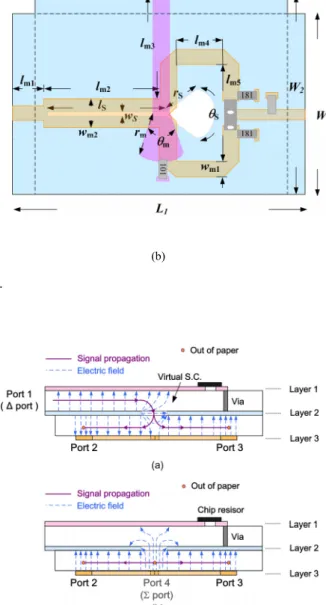
To design a compact multilayered magic-T with an even wider bandwidth, recently we discussed a new aperture coupled microstrip magic-T with a wideband microstrip-to-slotline Marchand balun [4]. The proposed design was fabricated on a low cost FR4 epoxy substrate to fulfill the cost reduction requirement. The circuit layout of the proposed magic-T is illustrated in Fig. 1(a). The proposed design consists of three metal layers. On the top layer (Layer 1), the microstrip line connected to port 1 is terminated with an open-circuited radial stub. A chip resistor is connected to the open end of the stub and provides the necessary current return path and resistive loading for the pulse generator attached to port 1.
The resistor also minimizes the multi-reflections between
(a) (b)
(c) (d) Fig. 3. Simulated and measured S-parameters of the proposed Magic-T.
the radial open stub and the cross-junction of the microstrip line and slotline. A microstrip T-junction along with a quarter-wavelength impedance transformer is printed on the bottom layer (Layer 3) of the magic-T. The layer in-between (Layer 2) is a common ground plane with a coupling slotline etched on it. A short-circuited radial stub is etched at one end of the coupling slot. Essentially, the microstrip line on the top layer and the slotline on the common ground plane form a wideband Marchand balun. It plays a key role in further broadening the operation bandwidth of the magic-T.
In the magic-T, the port 1 serves as the difference (∆)
port whereas the port 4 acts as the sum (Σ) port. The ports 2 and 3, on the other hand, are the output ports of the circuit.
Shown in Fig. 2(a) and (b) are the electric field distributions along the cross section A-A’ of the magic-T as the difference and sum ports are excited, respectively. The operation principles have been well explained in [4] and will not be repeated here for brevity. The proposed magic-T was designed using EM simulator Ansoft HFSS 10.1, and was fabricated on a multilayered FR4 epoxy substrate each with a thickness of 0.8 mm. The dielectric constant and loss tangent of the substrate are 4.4 and 0.022, respectively. The optimized dimensions are given as follows: L1 = 23 mm, L2
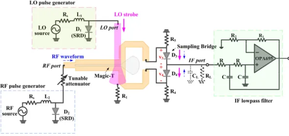
Fig. 4 Configuration of the proposed microwave sampler along with the pulse generators and active lowpass filter.
Fig. 5 Measured waveforms (a) at the RF port, (b) across the sampling diodes, (c) at the IF port, and (d) at the filter output of the microwave sampler.
= 19 mm, W1 = 23 mm, W2 = 25 mm, lm1 = 3 mm, lm2 = lm5 = 11 mm, lm3 = ls =12.5 mm, lm4 = 4.5 mm, wm1 = 1.5 mm, wm2 = 3.2 mm, ws = 1 mm, rs = 2.62 mm, rm = 4.74 mm, θs = 60 o, and θm = 45 o. For demonstration purpose in the laboratory, the two layers of FR4 substrates were initially fabricated independently, and the ground planes of substrates were jointed together by adhesive around the peripherals. The ground planes were kept electrically short-circuited to guarantee proper operation. The overall size of the magic-T is 25 by 23 by 1.6 mm3. The simulated and measured S-parameters are shown in Fig. 3. The measurement was taken by an Agilent E8362B network analyzer. The measurement agrees very well with the simulation. The measured return losses at all ports are better than 9.5 dB (i.e. VSWR < 2) from 1.5 to 7 GHz. The measured 3-dB insertion loss bandwidth between ports 2 and 1, i.e. S12, is 4.41 GHz. It corresponds to a fractional bandwidth of 94.2 %. The minimum insertion loss observed is 5 dB, which is 2 dB apart from the ideal value. The slightly higher insertion loss in the proposed design can be attributed to the lossy nature of the FR4 substrate used. The transmission coefficient at the sum port, i.e. S42 or S43, reveals a lower insertion loss of 3.7 dB. It also features a wider 3-dB insertion loss bandwidth from 0.5 to 8 GHz.
The isolation between the sum and difference ports is better than 35 dB over the frequency range of concern. Shown in Fig. 3(d) is the phase difference between the two output ports as the sum and difference ports are driven alternatively. Well-behaved phase response can be observed throughout the whole band.
3.THE MICROWAVE SAMPLER
By utilizing the proposed magic-T, we demonstrate a multilayered microwave sampler in this section. The
configuration of the proposed microwave sampler is shown in Fig. 1(b) along with the geometric parameters. Figure 4 illustrates the schematic diagram of the microwave sampler together with the pulse generators, sampling bridge, and IF lowpass filter. As shown in the figure, the pulse generator at the LO port periodically sends strobe signals for sampling the RF waveform. A pair of Schottky diodes with the same polarity is connected to the output ports, i.e. ports 2 and 3, of the magic-T. It forms a balanced sampling bridge. The sampling diode used is a low-barrier, low junction capacitance Schottky diode from M/A-COM® with part number MA4E2054-1141T. The IF signal is extracted in between the diode pair, and is terminated by a shunted RC tank. In practical application, the input impedance of the next stage can serve as the RC loadings.
The strobe signals at the sampling bridge are enabled by a shunt-mode pulse generator [19]. The pulse generator consists of a series inductor L1, a series resistor R1 and a shunt-to-ground step recovery diode (SRD) D1. The SRD applied here is a SMMD-0840 diode from the Metelics®
Cooperation. The shunt-mode pulse generator provides Fig. 6 Schematic diagram of the proposed impulse-radio-based ultrawideband RF front-end. (a) Transmitting module. (b) Receiving module.
Fig. 7 Configuration of the pulse generator and shaping network in the transmitting module.
Gaussian-like impulses at its output. The operating principle has been well explained in the literatures [4], [19] and will not be addressed here for the sake of simplicity. The proposed microwave sampler was also designed on a multilayered FR4 epoxy substrate. The design features a compact size of 25 by 28 by 1.6 mm3.
To validate the performance of the proposed microwave sampler, in the experiment we employ a similar shunt-mode pulse generator at the RF port. A tunable attenuator is inserted in-between the RF pulse generator and the magic-T to provide an adequate attenuation. It mimics the received waveform by the receiving module over air interface. Both pulse generators are driven by Agilent vector signal generators E4438C. The operating frequencies of RF and LO signals are 294.9 MHz and 294.4 MHz, respectively.
Figure 5(a) shows the measured waveform at the RF port of the microwave sampler. The measurement was taken by an Agilent real-time digital oscilloscope 54855A along with the 1134A probing system. The sampling rate is 5 GSample/s. The RF pulse has a peak voltage of -120 mV and the pulse width is 1 ns. Figure 5(b) depicts the
measured waveforms across the sampling diodes. The waveforms are with equal amplitude but reverse pulse polarity. The Gaussian-like strobe signals are converted into monocycle pulses at the diode junction due to multi-reflections. The monocycle waveform is more preferable since it can force the sampling diode to turn off rapidly and helps improve the sampling accuracy [9]. The pulse width of the sampling strobe is 380 ps, and the voltage difference across the diodes is higher than 1 V. The output waveform at the IF port is shown in Fig. 5(c). The IF signal actually consists of thousands of LO strobes. Each strobe signal was amplitude-modulated by the RF signal at the sampling period. The IF pulse has a peak voltage of -70 mV, which corresponds to a conversion loss of 9.4 dB in a 50-ohm system. The pulse width of the IF signal is 0.5 µs, and the repetition frequency is 500 kHz. Additionally, it is worthwhile to mention that owing to the nonzero reverse-biased junction capacitance of the sampling diode, the RF signals may AC couple to the IF port even when the sampling diodes are turned off. It gives rise to the RF leakage shown in Fig. 5(c). To filter out the high frequency
(a) (b) (c)
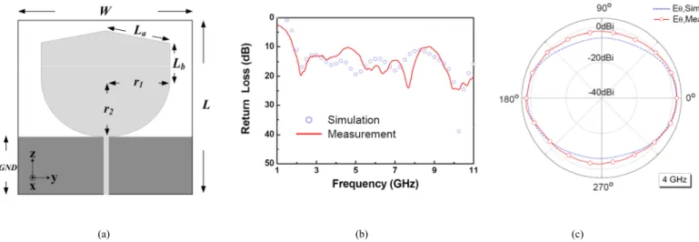
Fig. 8 (a) Geometry, (b) return loss, and (c) xy-plane radiation pattern of the planar monopole antenna for transceiving ultrawideband signals.
(a) (b)
Fig. 9 Photographs of the fabricated (a) transmitting module and (b) receiving module.
components arisen from both the sampling strobes and RF leakage, we implement an active filter at the output of the microwave sampler, as illustrated in Fig. 4. The operational amplifier used is from TI Corporation with part number OPA695. The cutoff frequency is 8 MHz and the DC gain is 2.2. The filtered-out signal is shown in Fig. 5(d). The peak voltage is -0.4 V and the pulse repetition frequency is also 500 kHz. It is evident that the sampled waveform at the IF port is quite similar to the RF input except that the time scale has been downscaled to the microsecond (µs) order.
Finally, it should be emphasized that in theory the RF waveform in the proposed microwave sampler could be an arbitrary periodical signal as long as the difference between the periods of the RF and LO signals is small enough to provide an adequate amount of sampling points.
4.ULTRAWIDEBAND RFFRONT-END MODULE
In this section, an impulse-radio-based ultrawideband transceiving module is demonstrated by implementing the multilayered microwave sampler. The proposed transceiving module aims at implementing in the RF front-end of a variety of ultrawideband systems such as in-vehicle communications, surveillance systems, and etc.
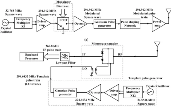
The schematic circuit diagrams of the transmitting and receiving modules are shown in Fig. 6(a) and (b), respectively. In the transmitting module, the CITIZEN®
crystal oscillator CSX-750FC generates a clock signal with
a clock rate of 32.768 MHz and peak-to-peak amplitude of 1.6 V. A TI® frequency multiplier SN65LVDS150 multiplies the clock frequency by a factor of 9. The multiplier is followed by a differential line driver SN65LVDT2DBVR to convert the differential signal at the output of the multiplier to a single-end one at the input of the modulator. The modulator is implemented by a TI®
single-pole-double-throw (SPDT) switch with part number TS5A3157. In the circuit implementation, we choose binary on-off keying due to its low circuit complexity. The baseband bitstream amplitude-modulates the 294.912-MHz square wave by controlling the modulator output. It allows the square wave to pass through when the bit is high. On the other hand, as the bit is low the modulator output is shorted to ground. To properly trigger the shunted-mode pulse generator, a feedback amplifier is attached to the output of the modulator to magnify the modulated square wave. The output signal has a peak-to-peak voltage of 5 V. Figure 7 shows the circuit configuration of the shunt-mode pulse generator along with a pulse shaping network. The pulse shaper consists of three resistive-loaded shunt stubs and two series lumped capacitors C1 and C2. In addition to serve as a resistive loading for eliminating the late-time ringing, the shaping network also acts as a second-order differentiation operator. By the differentiation operation, the pulse shaper can reallocate the spectrum of the incoming Gaussian pulse, which is known to have a large number of low-frequency Fig. 10 (a) Modulated pulse train at the output of the transmitting pulse generator. (b) Individual RF pulses in a single bit. (c) Sampled waveform at the IF port of the microwave sampler. (d) Output waveform at the filter output of the receiving module.
|1 LO 1 RF| 3.093 .
t f f ps
∆ = − =
components, to a higher frequency range. It therefore facilitates the transmission over air interface using an ultrawideband antenna with acceptable size. The pulse generator is optimized by the software Agilent ADS 2006.
The elements are given by L1 = 6.8 nH, R1 = 33 Ω, R2 = R3
= R4 = 12 Ω, C1 = 0.5 pF, and C2 = 1 pF. All the stubs are 1-mm-long 50-ohm microstrip lines. The pulse generating network is followed by a power amplifier, and the output modulated pulse train is transmitted to free space via an ultrawideband antenna. Figure 8(a) illustrates the antenna used for transmitting and receiving the modulated pulse train. The antenna is a planar monopole antenna developed in our laboratory. The bottom part of the radiator is described by an elliptical profile. It helps improve the impedance matching over a wide bandwidth. The pentagon on the upper part of the antenna may further lengthen the electrical current path and hence lower down the lowest operating frequency. The overall antenna size including the finite size ground plane is 60*60 mm2. The geometric parameters are La = 22.4 mm, Lb = 12 mm, r1 = 22 mm, r2 = 20 mm, and LGND = 20 mm. The simulated and measured return losses are shown in Fig. 8(b). The agreement
between the results is very well. The operating bandwidth with return loss better than 10 dB is from 2 to more than 11 GHz. The simulated and measured radiation patterns at 4 GHz, i.e. the center frequency of the pulse spectrum, are illustrated in Fig. 8(c). For simplicity here only the co-polarized component, Eθ, in the xy-plane is shown.
Referring to the figure, the antenna demonstrates quite omnidirectional pattern at the principal plane. The measured antenna peak gain, which occurs at the broadside direction, is 2.7 dBi.
The receiving module consists of a template pulse generator, a microwave sampler, and an active lowpass filter. In Fig. 6(b) the multilayered microwave sampler has been represented by its equivalent circuit model. The template pulse generator has a similar configuration to the shunt-mode pulse generator used in the transmitting module except that the frequency of the crystal oscillator is now 24.5536 MHz. By a multiplier factor of 12, the output clock rate is 294.6432 MHz. Unlike the transmitting module, however, here a pulse generator alone is adequate enough for generating LO strobes for sampling the received waveform. The strobe impulse converts into a pair of monocycle pulses with reverse polarity in the microwave sampler, as has been demonstrated in Fig. 5(b). The RF waveform received by the ultrawideband antenna is first divided into two branches by the T-junction of the sampler.
It is then periodically sampled by the strobe impulses at the balanced sampling bridge. According to the equivalent time sampling theory [6], the equivalent sampling interval between two consecutive samples can be evaluated by
(1) In other words, if the pulse width of the RF signal is 500 ps, every single pulse reconstructed at the IF output will consist of more than 160 samples. Accordingly, the receiving module is capable of downsampling subnanosecond pulses with high accuracy. An active filter is connected to the
Fig. 11 Experimental setup for demonstrating the proposed Fig. 12 Sampled waveforms at the output of the receiving ultrawideband RF front-end module over air interface. for various bit patterns.
Fig. 13 Received amplitude versus the separation distance between the transmitting and receiving antennas.
output of the microwave sampler to filter out the high frequency components. The cutoff frequency is 12 MHz and the DC gain is 2.2. The downsampled pulse train has a pulse repetition frequency of 268.8 kHz, and is now ready for baseband processing.
Photographs of the fabricated transmitting and receiving modules are shown in Fig. 9(a) and (b), respectively. The antennas are not shown in the photographs for brevity. For demonstration in the laboratory, the power amplifier connected to the transmitter is an AR amplifier 1S1G4A with an 18-dB gain. The bitstream is generated by an Agilent 33220A arbitrary waveform generator. Two data rates, 90 kbps and 270 kbps, are demonstrated in the following discussions. Figure 10(a) shows the modulated pulse train at the output of the pulse shaping network. The bit sequence has a repeated 1010 pattern with a data rate of 90 kbps. Each bit actually consists of 3,277 (i.e. 294.912 MHz/90 kHz) RF pulses each with a peak amplitude of 0.3 V. Figure 10(b) illustrates the individual RF pulses in a single bit. The RF pulse approximates to a second-order Gaussian derivative. The repetition frequency is 294.912 MHz and the pulse width is about 500 ps. To demonstrate sampled waveform in an ideal multipath-free environment, the transmitting and receiving modules were temporarily connected together by a coaxial cable. The power amplifier was temporarily removed as well. The waveform at the output of the microwave sampler is shown in Fig. 10(c). As shown in the figure, each bit consists of three downsampled second-derivative Gaussian pulses since the 90-kbps IF pulse train has a repetition frequency of 268.8 kHz. The filtered-out bitstream at the output of the lowpass filter is shown in Fig. 10(d). An enlargement of the downsampled pulse is shown in the inset as well. The output bitstream can be readily demodulated by a simple baseband processor.
Additionally, it is worthwhile to mention that the filtered-out waveform has a 60-mV DC offset, which is likely a result of the noise power in the circuit.
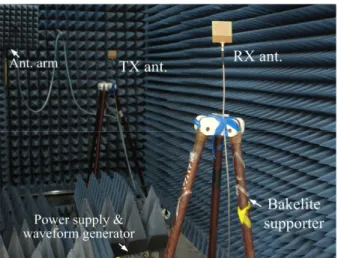
Figure 11 shows experimental setup for validating the transceiving module over air interface. The experiment was completed in an anechoic chamber at National Taiwan University of Science and Technology. Two abovementioned ultrawideband antennas were mounted on the bakelite supporters to transmit and receive the modulated pulse train. The separation distance between the antennas was 2.3 m. The instruments including the power supply, oscilloscope, arbitrary waveform generator, and etc.
were carefully shield by electromagnetic wave absorber to reduce multipath interference. The antenna arm in the background of the measurement setup, however, can be hardly shielded since the chamber is originally design for near-field measurement. Throughout the measurement the data rate is set to 270 kbps, which in turn implies that each filtered-out bit contains only one downsampled pulse.
Four repeated bit patterns, including 0101, 0111, 0001, and 0011, were fed into the transmitting module. The waveforms at the filter output are illustrated in Fig. 12. Due
to the limited space, the waveforms are offset by 0, 50, 100, and 150 mV to facilitate the plot in the same figure.
Referring to the figure, the outputs clearly demonstrate the desired bit patterns which can be readily demodulated by a baseband processor. Figure 13 illustrates the received amplitude versus the separation distance between the transmitting and receiving antennas. Both data rates are evaluated at four different separations, i.e. 0.35, 1.0, 1.65, and 2.3 m. Referring to the figure, the output waveform roughly follows the 1/R fading. The maximum transmitting distance is estimated to be 4.5 m since the minimum detectable threshold is 5 mV above the average value of the bit streams, as has been illustrated in Fig. 12. Finally, it should be emphasized that further increasing the transmission data rate can be accomplished in two ways.
Firstly, at the expense of a lower sampling accuracy, the data rate can be significantly improved by increasing the frequency difference between the RF and LO signals. For example, a transmission data rate of 2 Mbps is possible if the LO frequency is retuned to 292.912 MHz. However, the sampling points per reconstructed pulse drop dramatically from 160 to 21 points. Alternatively, if the frequencies of both LO and RF signals raise proportionally, the sampling accuracy can be retained while the data rate is effectively increased. For instance, the equivalent sampling interval is 8 ps if the LO and RF frequencies are set to 500 and 502 MHz, respectively. The resultant data rate will also be 2 Mbps but the sampling points per reconstructed pulse improve to 62 samples. The cost, nonetheless, rises accordingly since the clock generating circuit needs to be operated at a higher frequency.
5.CONCLUSION
An impulse-radio-based ultrawideband RF front-end module has been proposed and demonstrated in this paper.
The proposed transceiving module is developed based on a novel multilayered microwave sampler. The microwave sampler is composed of a wideband multilayered magic-T and a balanced sampling bridge. The microwave sampler features high sampling accuracy with a compact size of 25 by 28 by 1.6 mm3. By utilizing the equivalent time sampling theory and binary on-off keying modulation scheme, the proposed front-end module demonstrates a transmission data rate of 270 kbps with coverage up to 4.5 m. The tradeoff for increasing the data rate has been discussed in this paper as well. The proposed RF front-end module may find applications in various circumstances such as in-vehicle communications, surveillance systems, and etc.
The future work will be in improving the dynamic range of the microwave sampler, reducing the power consumption of the front-end module, and in developing more complicated modulation scheme to further increase the data rate.
IV.參考文獻
[1] G. R. Aiello and G. D. Rogerson , “Ultra-wideband wireless systems,” IEEE microwave, vol. 4, no.2, pp. 36-47 , June 2003.
[2] L. Yang and G. B. Giannakis, “Ultra-wideband communications: an idea whose time has come,'” IEEE Signal Processing Magazine, vol.
21, no. 6, pp. 26-54, Nov.2004.
[3] C. Fang, Y. Zheng and C. L. Law, “An ultra wideband transmitter based on up conversion architecture,” in Proc. IEEE Int. Workshop on Radio-Frequency Integration Tech., Nov. 2005, Singapore, pp.
38-41.
[4] T. G. Ma and C. F. Chou, “A compact multilayered magic-T in microstrip form and its application to microwave sampler,” in 2008 IEEE Int. Microw. Symp. Dig., Jun. 2008, Atlanta GA, pp. 887-890.
[5] K. A. Remley and D. F. Williams, “Sampling oscilloscope models and calibrations,” in 2003 IEEE Int. Microwave Symp. Dig., Jul. 2003, Philadelphia PA, pp. 1507-1510.
[6] R. Lawton, S. Riad, and J. Andrews, “Pulse & time-domain measurements, Proc. IEEE, vol. 74, pp. 77-81, Jan. 1986.
[7] K. Madnani and C. S. Aitchison, “A 20GHz Microwave Sampler,”
IEEE Trans. on Microw. Theory Tech., vol. 40 , no. 10, pp.
1960-1963, Oct. 1992
[8] K. Madani, “A hybrid 0.5 - 20 GHz microwave sampler,” in IEE Colloquium on Multi-octave Microw. Circuits, Nov. 1991, London UK, pp. 3/1-3/4.
[9] J. Han and C. Nguyen, “Coupled-slotline-hybrid sampling mixer integrated with step-recovery-diode pulse generator for UWB applications,” IEEE Trans. on Microw. Theory Tech., vol. 53, no. 6, pp. 1875-1882, June 2005.
[10] J. Ohm, and M. Alberty, “Microwave phase detectors for PSK demodulators,” IEEE Trans. on Microw. Theory Tech., vol. 29, no. 7, pp. 724-731, Jul. 1981.
[11] B. Stec, C. Recko, and W. Susek, “Multibit microwave frequency discriminators,” in Proc. 2006 Int. Conference on Microw., Radar &
Wireless Communications, May 2006, pp. 240-242.
[12] D. M. Pozar, Microwave Engineering, 3rd ed., John Wiley & Sons, 2005.
[13] J. P. Kim and W. S. Park, “Novel configurations of planar multilayer magic-T using microstrip-slotline transitions”, IEEE Trans. Microw.
Theory Tech., vol. 50, no. 7, pp. 1683-1688, July 2002
[14] K. U-yen, E. J. Wollack, J. Papapolymerou, and J. Laskar, “A broadband planar magic-T using microstrip–slotline transitions,”
IEEE Trans. Microw. Theory Tech., vol. 56, no. 1, pp. 172-177, Jan.
2008.
[15] L. Fan, C.-H. Ho, S. Kanamaluru and K. Chang, “Wide-band reduced uniplanar magic-T, hybrid-ring, and de Ronde’s CPW-slot couplers”, IEEE Trans. Microw. Theory Tech., vol. 43, no. 12, pp. 2749-2758, Dec. 1995.
[16] S. Gruszczynski, K. Wincza, and K. Sachse, “Design of compensated coupled-stripline 3-dB directional couplers, phase shifters and magic-Ts (part II: broadband coupled-line circuits),” IEEE Trans.
Microw Theory Tech., vol. 54, no. 9, pp. 3501-3507, Sep. 2006.
[17] M. W. Katsube, Y. M. M. Anter, A. Ittipiboon, and M. Cuhaci, “A novel aperture coupled microstrip magic-T”, IEEE Microw. Guided Wave Lett., vol. 2, no. 6, pp.245-246, June 1992.
[18] M. Davidovitz, “A compact planar magic-T junction with aperture-coupled difference port,” IEEE Microw. Guided Wave Lett., vol. 7, no. 8, pp. 217-218, August 1997.
[19] R. Hall, S. Hamilton and S. Krakauer, “Impulse-Shunt Made Harmonic Generation,” in Proc. 1966 ISSCC, pp. 66-67.
計畫編號:NSC 96–2221– E–011–008 執行期限:96 年 08 月 01 日至 97 年 07 月 31 日
計畫主持人:廖文照 助理教授 國立台灣科技大學 電機工程系 計畫參與人員:李威漢、王景平、游勝傑
1. 前言
本計畫考量特殊的車輛電磁傳播環境如金屬車 體屏蔽、鄰近脈衝雜訊源以及高溫的物理特性,開發 可達傳輸需求並符合經濟效益的天線構型設計。同 時,由於本計劃所搭配之其他子計畫係利用LTCC 多 層技術製程射頻晶片,故亦考量天線與射頻電路整合 時所產生的電磁相容(electromagnetic compatibility)、
電磁干擾(electromagnetic interference)問題。
本子計畫所研究之工作項目主要有兩項:其一為 評估車用防撞雷達操作時的 FMCW 回波特徵變化;
另一項則是研發利用電磁脈衝技術進行無線通訊所 需的超寬頻天線,並評估超寬頻脈衝訊號在車輛引擎 室內與車廂內的傳播特性,該研究可因應車內各式感 應器與車內微控制器(micro control unit, MCU)的通訊 需求。
本計畫研究之車用防撞雷達回波評估係指利用 隱藏於車輛前方保險桿內的平面式、窄頻、指向性、
高 增 益 天 線, 採 取 雙 頻連 續 波 雷 達(two frequency continuous wave radar, CW radar)形式偵測前方車輛或 固定障礙物的回波特徵。我們利用高頻數值電磁模擬 方法(NEC-BSC code),模擬出不同的車輛遠近距離與 姿態時的回波分佈量值及其相位變化。在模擬模型中 採用單一高指向性的發射天線與多個接收天線位 置,在利用訊號處理方法校正發射到接收天線的背景 耦合量後,可比對各觀察點所接收的回波量大小判斷 出目標物的縱向距離、橫向位移,甚至是車身的姿態 角度。該結果可作為未來發展防撞雷達目標物定位、
定向與行進方式推估演算法之用。
2. 文獻探討
超寬頻訊號於複雜環境的傳播
超寬頻(UWB)傳輸技術的觀念最早由馬可尼於 1895 年發明,而現代超寬頻無線通訊技術是從 1960 年代開始並且於1970 至 1980 發展[1]。FCC 於 2002 年 2 月 14 日發佈免執照授權的 UWB 使用規範,將 3.1 GHz 至 10.6 GHz,共 7,500 MHz 頻段配置給 UWB 裝置使用[1],該規則對於不同類的 UWB 設備,定義 了其發射功率限制,大致上所有頻帶的傳輸功率都限 制在-41 dBm 以下。近年來在無線個人區域網路
(WPAN)特別是高速率傳輸上扮演領導性技術,可 提供多媒體影音傳輸,在10 公尺的傳輸範圍內,可替 代纜線作為影像或聲音的傳輸媒介[1]-[2]。
寬頻傳輸環境的相關研究已經相繼發表,像是超 寬頻訊號在桌上型電腦環境裡的傳播、室內筆記型電
腦對於超寬頻訊號的遮蔽效應以及車輛的衰減量測等 [2]-[4]。然而沒有特別針對車輛引擎蓋下方的研究。
有鑑於此,本研究提出一個模擬與實際量測同時運用 的方式,以去檢測寬頻訊號在具障礙物環境下的傳播 特性。透過網路分析儀,可以記錄下2~6 GHz 此寬頻 範圍的插入損失S21,並使用數值軟體 MATLAB,將 頻域響應轉換到時域上,合成一個極短暫的脈衝訊 號。透過此脈衝訊號的分析,我們可以辨識出發射天 線到接收天線之間環境狀況,並且分析出它在不同的 電磁波散設環境,傳輸效能的優劣。
調頻連續波於汽車防撞雷達環境之回波評估
近年來車輛在正常行進模式下所使用的前方雷 達防撞系統,多採用以毫米波雷達或光學式雷射雷達 技術為主。紅外光在大氣環境中效能時常受到天候的 影響,而使用頻域調變連續波(frequency modulated continuous wave, FMCW)的毫米波防撞雷達不但可用 都卜勒效應計算目標物速度,且可用於計算目標物距 離[9,10]。此外亦可使用脈衝雷達測量目標物距離,利 用計算電磁波行進所造成的相位(時間)延遲,透過頻 域時域的互相轉換找出目標物散射源的幾何對應關 係,但脈衝雷達的原理乃是使用一超寬頻天線來發射 時域的脈衝,因此花費功率大,現階段在發射機技術 與成本上仍有改善的空間。而 FMCW 雷達相對在發 射機元件技術上較為成熟[11]。但須克服的是電磁波 在空中因多重路徑干擾而難以量化的技術問題[12]。
3. 研究方法
寬頻天線設計與效能驗證
在天線的設計上,為了達到寬頻的效果,我們使 用一片截角矩形金屬作為輻射體[5],並採用微帶線的 架構饋入。在天線效能驗證上,我們量測S11 反射係 數頻譜,最後在利用無反射實驗室量測天線輻射場型。
天線使用FR4_epoxy 板材,板厚 1.6 mm,介電係 數為4.4,損失正切為 0.022,其架構如圖三所示,天 線上半部截角矩形輻射體是由50 ohm 微帶線(L2)
饋入,背面金屬地面大小W3 × L2。經電磁模擬軟體 (HFSS10.0)優化後的設計參數是 W1 = 22.5 mm、W2 = 3.4 mm、W3 = 30 mm、L1 = 18.75 mm、L2 = 11.5 mm、
L3 = 35 mm、L4 = 3.29 mm,圖四是模擬出的反射損 失。模擬結果中反射損失小於-10 dB 的頻段範圍從 2.8 延伸到6.3 GHz,比我們需求的頻段從 2 到 6 GHz 偏 為高,所以使用60 mm × 60 mm FR4 的基版製作天 線,以預留調整操作頻段的空間。
以低溫共燒陶瓷技術研製車用防撞感測系統之射頻關鍵模組-
子計畫四:車用微型晶片天線與電磁傳播環境特性研究
圖三: 超寬頻單極天線架構
圖四: 模擬反射損失 S11
實作成品如圖五(a),由於量測的反射係數頻帶的 確偏向高頻,因此使用銅箔貼紙,將截角矩形輻射體 部分分別貼大為原來兩倍,與三分之四倍,如圖三 (b)。圖六是三者的反射損失結果,發現三分之四大小 的反射損失從2 到 6 GHz 都有在-7.14 dB 以下,所以 用它來作為發射及接收天線。天線輻射場型如圖七所 示,E-plane 上的 co-pol 最大增益值出現在 Phi = 0°與 150°,表示有往前的能量分布以及往後上方的能量分 布,並且以垂直極化為主,最大值有3.3 dB。而 H-plane 上的co-pol 顯得比較平均,而 cross-pol 在 4.5 到 6 GHz 的可實現增益值變大,可見有水平極化分量存在,但 增益值不大,在1.3 dB 以下。故此天線以垂直極化為 主,可把它看成是一支垂直擺放的超寬頻單極天線。
(a) 原型天線 (b) 調整後原型天線 圖五: 超寬頻單極天線實作
圖六: 原型天線反射損失頻譜
(a) E-plane, Co-pol (b) H-plane, Co-pol
(c) E-plane, Cross-pol (d) H-plane, Cross-pol 圖七: 天線輻射場型
傳播實驗模型的建置與模擬方法
在傳播實驗模擬模型的建置上,我們將網路分析 儀連接到先前製作的兩支寬頻單極天線上,視為訊號 進出的Port 1 與 Port 2。我們建置有多個不同的傳播 環境,圖八(a)所示環境定義為「No Ground」。而圖 八(b)中是加上長寬高分別為 91 cm × 46 cm × 88 cm 的 台車。台車上面的金屬平面可當成是地面,因此這個 情況設定為「Add Ground」。收發天線分別位於台車 邊緣的中間正上方處,距離台車10 cm 的高度。最後 我們把貼滿鋁箔紙的金屬箱放在台車上面,作為中間 障礙物,箱子中心位置對準地面的中心,金屬箱大小 為19 cm × 26 cm × 29 cm,如圖九。由於金屬箱有六 種擺設的擺設情況,因此我們先以高度(H)分,再以寬 度(W)分,共分作六種 Case,並定義長度為 L。
實驗步驟分兩階段處理,第一階段是作量測,我 們用網路分析儀掃瞄2 到 6 GHz 的頻率範圍,取 801 點,得到傳播的頻率響應頻譜。從頻域結果,可以知 道頻率在不同環境中衰減的情況。第二階段再把量測 到的頻譜結果作傅立業轉換,得到時域上的分布。從 時域上,我們可以更容易且直接的去分析它的大小以 及位置的變化。
(a) No Ground (b) Add Ground 圖八: 傳播實驗模型建置
![[102-2] WNFA lab4 - A Tiny Wireless Sensor Network 2014/5/12 Chih-Hsien Ou](data:image/gif;base64,R0lGODlhAQABAIAAAP///wAAACH5BAEAAAAALAAAAAABAAEAAAICRAEAOw==)