Research Express@NCKU - Articles Digest
Research Express@NCKU Volume 4 Issue 8 - June 6, 2008
[ http://research.ncku.edu.tw/re/articles/e/20080606/5.html ]
Self-assembly nanostructures probed by
scanning tunneling microscopy
J. C. A. Huang
Distinguished Professor, Physics Department and Associate VP of ORD of National Cheng-Kung University
Email: [email protected]
Appl. Phys. Lett. 89, 221915-221917 (2006)
A
bstractThe development of scanning probing microscopy since 1982 has led to the extensive investigation for the nanotechnology. Self-assemble nanostructures have been expected as promising for application of many advanced technologies. In this work, we will present the introduction of the nanotechnology related to scanning tunneling microscopy, particular on our study of self-assembly vicinal surface probed by scanning tunneling microscopy.
1. Introduction:
In recent years, nano materials and nanotechnology has been extensively studied by many scientific research groups in the world. Actually, the application of nano materials such as for catalyst and painting materials has existed for hundred years. There are many nano effects in the nature world. For instance, the surface of the lotus leaves have particular nanostructure; seashells employed organic materials as substrate to self-assemble inorganic/organic composites. The nano magnetic particles like compass exist inside bee’s bodies. These interesting and special phenomena are related to the nano effects.
In 1959, the Nobel Laureate in Physics- Richard Feynman gave a lecture in California institute of technology. In the lecture, he addressed that the possibility of manipulation in atomic scale based on physics theorem. Besides, he said that “Why cannot we write the entire 24 volumes of the Encyclopedia on the head of a pin? ”
Fig1. Atomic manipulation by STM
In 1990, the IBM scientists successfully arranged thirty five xenon atoms to form the letters ‘IBM’ (as seen in Fig1.), which confirms Feynman’s ideas. Nevertheless, the major cause which promotes
nanotechnology is wide-advance of analytic instrument in 80’s, such as scanning tunneling microscope (STM), Atomic Force Microscope (AFM), and Near-Field Microscope (NFM), etc. These microscopic instruments allow physical and chemical characterization of materials in nanometer scale. Particularly, Binnig and Rohrer invented collectively first atomic-resolution surface analytic instrument- STM in 1982. The invention of STM opens a new nanotechnology era.The wide-ranging impact of STM was undoubtedly responsible for the very rapid award of the Noble Prize in Physics to the inventors of the STM in 1986.
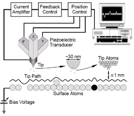
2. Scanning tunneling microscopy
The idea of STM comes from the “topografiner” developed in the early 1970’s (Young et al., 1972), that included most of the elements of an STM but can only operate with a larger tip-to surface gap (>1 nm, at which distance electron transport occurs via field emission). Deficiencies in both the mechanical and electrical systems at 1970’s limited the resolution to a few nanometers vertically and ~0.5 μm laterally. These problems were overcome ten years later by Binnig and Rohrer at the IBM Rüschlikon laboratory. They succeeded in creating an instrument with stable vacuum tunneling and precision scanning
Research Express@NCKU - Articles Digest
Fig.2 Photographs of a commercially available STM (AutoProbe VP, Park Scientific Instruments). (a) A ultra-high vacuum system. (b) STM stage mounted on vacuum flange. (c) a close look of STM showing the tip holder being transferred to the scanner.
Fig. 3 Basic elements of scanning tunneling microscopy
Our STM system is manufactured by Park Scientific Instruments (AutoProbe-VP), as shown in Fig 2. Figure 3 illustrates a sharp metal tip which is brought within 1 nm of the surface of an
electrically-conductive sample and a few volts are applied enabling electrons to quantum-mechanically tunnel across the tip-surface gap. The resulting tunnel current, typically on the order of 1 nA, depends exponentially on the gap: a change of 0.1 nm causes the current to change by a factor of about 10, thus giving STM atomic-scale sensitivity.
Research Express@NCKU - Articles Digest
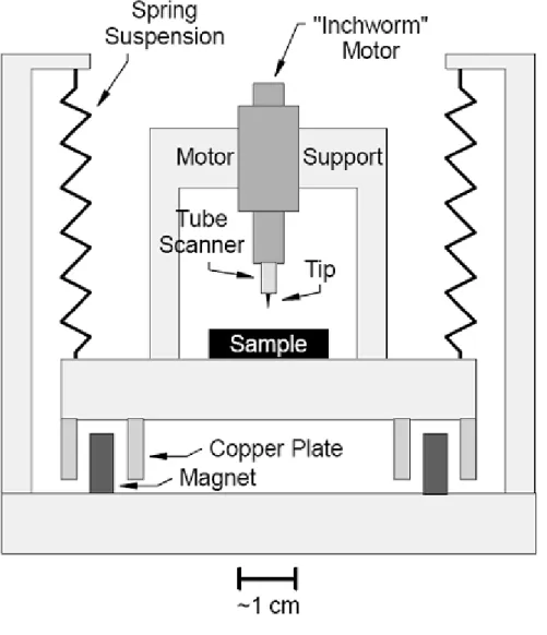
Fig. 4 shows the operating principles for two common coarse approach mechanisms of STM tip: (a) An “inchworm” motor employs a piezoelectric tube (PZT) and piezo-clamps to move an inner shaft with a series of clamping/unclamping and extension/retraction events. (b) Inertial motion of a free mass can be achieved by asymmetrical acceleration.
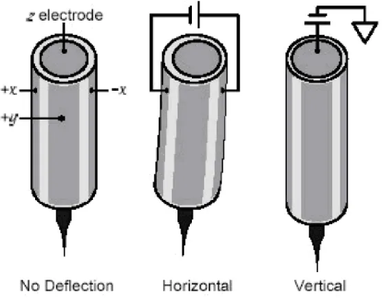
Fig. 5 Schematic sketch for operation of a piezoelectric tube scanner
The design of a typical tube scanner is shown in Fig. 5. A thin-walled tube of PZT is coated with metal on the inner and outer surfaces, with the outer surface divided into four equal quadrants by narrow metal-free regions. The inner surface is then used as the electrode for the vertical displacement (z), and the opposing pairs of outer electrodes are used for lateral motion (x and y). In this geometry a voltage applied between the inner and outer electrodes causes the tube to change length. Opposite voltages applied across opposing outer electrodes will induce one side of the tube to contract and the other to expand, causing a net lateral displacement (along with a small vertical displacement that can usually be ignored).
Fig. 6 Common elements of an STM, including a tip mounted on a piezoelectric tube scanner, a coarse approach mechanism (in this case an “inchworm” motor), and a damped vibration isolation system.
To achieve atomic-scale resolution, the mechanical and electrical components of a STM must enable the tip to be positioned within approximately 1 nm above the surface and then controlled both vertically and laterally with a precision of <0.01 nm. This precision requires low-vibration mechanical systems
combined with low-noise electrical circuitry. Several different ways have been developed to achieve the required mechanical stability; the common elements of such setup are illustrated in Fig. 6. STM requires a coarse approach mechanism capable of bringing the tip into tunneling range with the sample. Once in range, a scanning transducer controls the vertical and lateral position of the tip over the sample. The sample and scanner are mounted in a rigid framework to minimize the effect of mechanical resonances.
Research Express@NCKU - Articles Digest
Fig. 7 Biological sensors (left) and Chemical sensors (right)
Fig. 8 schematic sketch for nano-wire formed through step-flow growth (left);STM images and cross-section profile for Co nano-wire grown on Cu vicinal surface (right)
Nanostructures fabricated by top to down approaches are often restricted in size (using for example optical lithography) or in area (using for example e-beam or scanning-probing-microscopy lithography). Self-assembly is one of the noble techniques to reduce the size of nanostructures. For example, one can grow one-dimension (1-D) nanostructures on a vicinal surface with nano steps terraces. Under
appropriate conditions, 1-D nanostructures would be possibly prepared on the terrace edges through the step-flow growth mode, as shown for example in Fig. 8.
This method not only can provide an ordered arrangement for the deposited atoms but also reduce the dimensions to nanometers scale. Traditionally, vicinal surfaces are fabricated by mis-cutting a single crystal along certain high-index crystallographic planes. However, the precision limit by polishing procedures often leads to step bunching and inhomogeneous terrace width for miscut vicinal surfaces, as shown in Fig. 9. This disadvantage would severely influence the uniformity of nanostructures. In order to avoid these problems, the self-assembly vicinal surface (SAVS) could be a better template to fabricate nanostructures. Furthermore, the SAVS might produce much smaller terraces with single atomic step height for advanced nano-applications.
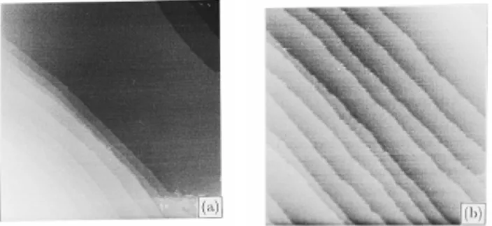
Fig. 9 Step bunching surface of Cu(111): (a)3000Å×3000Å(b)1000Å×1000Å
In this letter, we report the tilt growth and the formation of the SAVS of Mo(001) on Al2O3(1102)
substrate. The scanning tunneling microscopy (STM) and electron diffractions indicate the Mo SAVS with average terraces arranged along the [110]Mo direction. The statistical distribution for terrace width
of the Mo SAVS shows a narrow dispersion, as shown in Fig. 10. We propose that the formation of Mo SAVS is a consequence of a tilt growth of Mo(001) plane on Al2O3(1102) substrate because of asymmetric
lattice mismatch. By simple geometric calculation we also estimate the terrace width and the tilt angle of the Mo(001) SAVS, which is consistent with the experimental results. In this work, we correlates the tilt growth behavior with the formation of the SAVS of Mo(001) surface.
Research Express@NCKU - Articles Digest
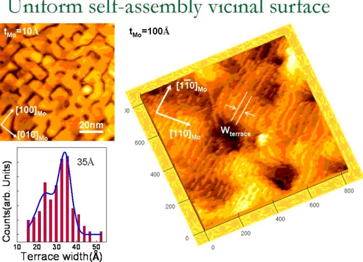
Fig. 10 STM images for (a) 10Å and (b) 100Å Mo films grown on Al2O3(1102) substrates. The statistic
distribution for the terrace width of the Mo(001) SAVS is shown in (c). The scan area of (a) and (b) is 100nm×100nm.