THlA-4
A Locally Matching Technique
for Broadband F
Design
*
ip-c hip Transit ion
Chun-Long Wang and Ruey-Beei
Wu
Department
of
Electrical Engineering and Graduate Institute of Communication Engineering, National
Taiwan University, Taipei, Taiwan, 106
17, ROC
Abstruct
-
A locally matching technique is proposed in this paper to improve the wideband performance of flip-chip transition. The gap width of the CPW line in the flip-chip bump pad region is enlarged for achieving larger inductance to compensate the capacitance at the transition, making the approximate impedance close to 50n.
An equivalent circuit is derived from the frequency response of the transition simulated by Sonnet and is used to control the resonance frequency of the structure. With properly chosen value of the enlarged width, the resonant dip can be controlled to improve return loss over a band from DC to 60GHz. Measurement data of the scaled structure is in good agreement with the simulation results, which validates the proposed design idea.I. INTRODUCTION
Flip-chip transition has become a promising technique over bond-wire in the microwave and millimeter wave frequency, due to its features of short and stable electrical interconnection, low cost, and high reliability. As
frequency goes higher, the parasitic effects of the flip-chip transition may result in performance degradation. They should be considered carefully in order to achieve good transition from DC up to millimeter wave spectrum.
For flip-chips of typical dimensions, the frequency response has been examined to yield an accurate equivalent circuit model which shows overall capacitive property [l]. It was thus suggested that the bump pad be kept as short as possible to lessen the capacitance at initial design [2]. This usually causes great concern in fabrication. Another approach was a staggered design in the central line of CPW [3]. The return loss was improved, but with the increase in the chip areas as trade off.
Recently, some investigators suggested to use a high impedance line or matching circuits on the motherboard to compensate the excessive capacitance of the transition [4]-
[6]. These techniques are satisfactory to optimize the transition over certain frequency band, but difficult to cover a wide band from DC up to millimeter wave spectrum. One way to enhance the transition bandwidth is to reduce the longitudinal dimension of the high impedance line or the matching circuits. Based on this concept, a locally matching technique is proposed in this paper by designing the transition transversely rather than
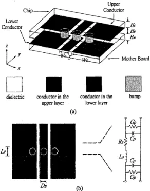
U p p r Conductor
Lower
A
Conductor /
U
dielectric conductor in the conductor in the bump
lower layer
upper layer
n n
( 4
@I
Fig. 1. The structure ofthetraditional flip-chip transition (a) 3-D view (b) upper view and its equivalent circuit. We200pm, S=70pm, We600pm, H e H ~ = H s 1 2 7 p ,
DB=160pm, Lp=200p, E ,=10.2.
longitudinally. Both the simulation and measurement are performed and compared to validate the design concept.
11. COMPENSATION ON ONE SLDE A . Hi-impedance compensation
Consider the structure of a traditional flip-chip transition snown in Fig. l(a). Fig. l(b) shows its top view together with the equivalent circuit which resembles a low pass filter of order N=3. The element values can be determined
*
This work was supported in part under the Grant 89-E-FA06-2 by Ministry of Education and NSC 90-221 9-E002-005 by National Science Council. Republic of China.1397
-
tradnionalequivalent drcuil 100 Ohm hi inpedance line
- - -
0 1 0 m 3 0 4 4 s o w
Frequency (GW
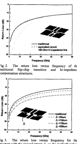
Fig. 2. The retum loss versus frequency of the traditional flip-chip transition and hi-impedance compensation structures. A A=I50um A =m)um 60 0 1 0 m 3 0 4 0 5 0 6 0 Frequency (-1
Fig. 3. The return loss versus frequency for the structure with the ground retreat A on the motherboard as
a parameter.
from the comparison with the frequency response of the transition simulated by Sonnet. It is found that the series resistance
R,
and shunt conductance Gf are small and can 1, the series inductance Ls is found to be 69.95pH and the shunt capacitance Cp is 34.81fF. Since Z, = , / m + 3 2 R is much smaller than the system of characteristic impedance z0=50R,
the transition shows overall 'capacitive property.Fig. 2 compares the simulation results of return loss (RL) for the traditional flip-chip transition and those by the equivalent circuit in Fig. l(b). The agreement verifies the correctness of such an equivalent circuit. The results by adopting the hi-impedance compensation technique [ 5 ] - [ 6 ] is also shown on this figure. It is clear that the return loss is improved at low frequency band only. From an equivalent circuit point of view, the addition of hi- impedance line which contributes a large series inductance to form a low pass filter with order N=4 will degrade its high frequency performance. In addition, the overall effect be neglected. With the geometric dimensions given in Fig.
Fig. 4.
of the locally matching structure.
The return loss versus frequency for the structure of the hi-impedance line is no more a lumped inductance when its length reaches one-tenth of a guided wavelength at high frequencies.
B. Increasing the gap width on motherboard
Td improve the high frequency performance of the flip- chip, the values of the series inductance Ls and the shunt capacitance Cp should be carefdly controlled. Intuitively, a good transition can be achieved if both the values of the series inductance or shunt capacitance are reduced to make the associated impedance Z, =
,/m
matched to 50 Q.Subject to the constrain by the wiring rule in the fabrication process that the length and aspect ratio of bump is maintained, the value of the inductance could not be reduced by this way. The remaining way is to reduce the value of the shunt capacitance in the discontinuity. Fig.
3 shows the simulation results of return loss in which the
gap width on the motherboard is enlarged to reduce the shunt capacitance. It can be seen that the retum loss is improved with a suitable gap width, as evident from the equivalent circuit in Fig. 1 (b). It deserves mentioning that the improvement covers a large bandwidth since the matching structure occupied a very small area.
However, the overall capacitance of the discontinuity is contributed by the shunt capacitance Cf on both the motherboard and the chip sides. Reducing the capacitance on one side only will restrict the effectiveness of this design. Thus, it would be better to employ the idea of locally matching to reduce the values of the capacitance on both sides more efficiently.
111. COMPENSATION ON BOTH SIDES
The locally matching structure is shown in the inset of Fig. 4. It is seen that both the ground conductor on the 'motherboard and chip are retreated by a distance A. Fig. 4
also shows the frequency response of return loss with
,"t
I A =150um 0 1 0 2 0 3 0 4 5 0 6 0'.
; I !;. ,
.
A-m Frequency (GW 6 0 " 1 I IFig. 5. The retum loss versus frequency for the equivalent circuit of the locally matching structure.
0 so 1W 150
Ground Retreat A (um) Fig. 6 .
versus the ground retreat A .
The series inductance Ls and shunt capacitance C,
ground retreat A as a parameter. By properly choosing the parameter, say A=100 pm, the retum loss can be greatly improved over a wide band covering DC up to 60 GHz or more. The design is satisfactory and simple, but with some areas occupied in the transverse direction of the chip as trade off.
The equivalent circuit of the locally matching structure can be well represented as Fig. l(b) including the effect of the step discontinuity since the size of the discontinuity is small as compared to one-tenth of the guided wavelength. The retum loss of the equivalent circuit versus frequency is shown in Fig. 5. The excellent agreement with those in Fig. 4 verifies the correctness of this equivalent circuit. Fig. 6 shows the result of the series inductance Ls and shunt
capacitance
Cp
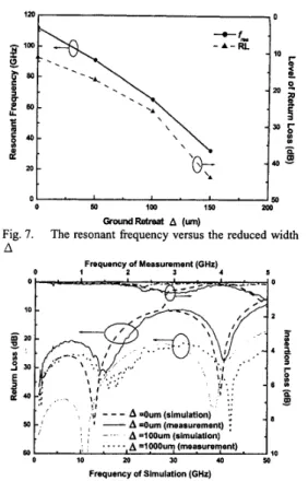
versus the ground retreat A. As A increases, the capacitance decreases as expected while the inductance increases. Actually, A has a more significant influence ob the series inductance than on the shunt capacitance.It is interesting to note the occurrence of the dip in the retum loss versus the frequency for A=15Opm in Fig. 5. The resonant frequency, which corresponds to the dip of
0 50 1M 150 100
GrwndRetreal A (um)
Fig. 7.
A
The resonant frequency versus the reduced width
Frequency of Measurement (GHz) 0 1 2 3 4 5 0 10
-
1;- - -
A =Oum (simulation) ~ '-
A =Oum (measurement) : - A =100um (simulation) ... A =1000um (measurement) 8 50 - ' 60 i o 0 10 20 30 4 50 Frequency of Simulation (GHz)Fig. 8. Frequency response of the back-to-back transition structure for the comparison between simulation results and measurement data of ten times scaled model.
retum loss can be derived from the equivalent circuit of Fig. l(b). There are two solutions, one isf=OGHz and the other is:
At the open circuit limit that Z, tends to
-,
the resonant frequency becomes f,cs = d m / 2 r r which corresponds to the resonance in the transverse direction of the flip-chip transition. Fig. 7 shows the value of resonant frequencyversus the ground retreat A. It can be seen that the value of
the resonant frequency corresponding to A=200pm does not exist because the value of ZD is large than 50R. Also shown in this figure is the level of retum loss, which is defined as the local minimum of retum loss before the resonant frequency
f,,
for a given value of A in Fig. 5.Based on this figure, the ground retreat A can be chosen lproperly to determine the resonant frequency
f,,
for the best transition performance over the desired bandwidth.For experimental verification, two single locally matching structures are fabricated and connected back to back for measurement with ten times scaled up in all the geometric dimensions. The separation between the two single transitions is 22mm, which results in a multiple resonance frequency of 3.16GHz. The circuit is fabricated on the board of RT/Duroid 6010 and bump is formed with copper. The measurements are done on the Vector Network Analyzer HP85 1OC with the TRL calibration.
Fig. 8 shows the frequency response of the back-to-back
transitions obtained by the simulation and measurement under ten times model. Good agreement between simulation and measurement can be seen from the figure except for a small shif? in the resonance frequency. This may be contributed to the abrupt cut of the dielectric of the chip near the discontinuity or the misalignment of solder bumps in fabrication. For the insertion loss, the measurement shows the same tendency as the simulation results if the conductor and dielectric loss are not concerned.
IV. CONCLUSIONS
The hi-compensation structure can improve the performance of the flip-chip transition only in a limited frequency range due to its comparatively large size in longitudinal direction. The locally matching technique with ground retreat A on the motherboard only can
improve the return loss of the flip-chip, but the effectiveness is restricted by the capacitance of the discontinuity on the chip side. The idea of locally matching is also extended to both the motherboard and the chip sides in this paper. By properly choosing a suitable ground retreat A to control the resonant frequency, the return loss of the flip-chip transition can be greatly improved over a wide frequency band with some occupied area on the transverse direction of chip as trade off.
ACKNOWLEDGEMENT
The authors would like to thank Mr. Shih-Chieh Yen and Shih-Je Yang for helps on the circuit board fabrication and Mr. Wen-Hua Tu for the suggestions in measurement.
REFERENCES
[I] H. H. M. Ghouz and E. El-Aharawy, "An accurate equivalent circuit model of flip chip and via interconnects,: IEEE Trans. Microwave Theory Tech., vol. 44, no. 12, pp.
2543-2554, Dec. 1996.
[2] M. Szymanowski and S . Safavi-Naeini, "Characterization of a flip-chip interconnect at frequencies up to 30 GHz," 2000 Canadian Conference on Electrical and Computer Engineering, vol. 2, pp. 784-787,2000.
[3] H. H. M. Ghouz and E. El-Aharawy, "Finite-difference time-domain analysis of flip-chip interconnects with staggered bumps," IEEE Trans. Microwave Theory Tech., vol. 44, pp. 960-963, June 1996.
[4]
N.
Iwasaki, F. Ishitsuka, and K. Kato, "High performance flip-chip technique for wide-band modeles," 1996 IEEE 5thTopical Meeting on Electrical Performance of Electronic Packaging, pp. 207-209, 1996.
[5] W. Heinrich, A. Jentzsch, and G. Baumann, "Millimeterwave characteristics of flip-chip interconnects for multi-chip modules," IEEE Trans. Microwave Theory Tech., vol. 46, pp. 2264-2268, Dec. 1998.
[ 6 ] A. Jentzsch and W. Heinrich, "Theory and measurement of flip-chip interconnects for frequencies up to IOOGHz," IEEE Trans. Microwave Theory Tech., vol. 49, pp. 871-811, May, 200 1.