Bias-Dependent Charge Accumulation in Pentacene-based Thin-Film
Transistors
Chi-Feng Lin
a, Kai-Hsiang Chuang
a, Yet-Min Chen
a, Jiun-Haw Lee
*a, Jian-Jang Huang
a,
and Yu-Wu Wang
ba
Graduate Institute of Electro-Optical Engineering and Department of Electrical Engineering,
National Taiwan University, No. 1, Sec. 4, Roosevelt Road, Taipei, Taiwan, R.O.C.
b
Electronics Research & Service Organization, Industrial Technology Research Institute, Hsinchu,
Taiwan 310, ROC
ABSTRACT
In this paper, we have demonstrated the current increase with repeated measurements of Id-Vds curves with different Vg
values which results from the non-uniform carrier accumulation in the channel region of a pentacene-based thin film transistor (TFT). The mobility of our device reaches 0.07 cm2/Vs even the substrate was not heated during pentacene deposition. Besides, the devices show good air-stable properties. The magnitude of Id decreased less than 30% after
exposure in air for 2 weeks. By repeating the Id-Vds measurements from 0 to -50 V with the Vg values of 0, -10, -20, -30,
-40, and -50 V for 10 minutes, we observed a four times current increase from -0.75 to -2.8 µA at Vg= -50V and Vds
=-50V. The current increase comes from the holes accumulation near the drain. When the source and drain were exchanged, the current decreases to the 0.08 µA. After another 10 minutes operation, the current will recover back to the original values. Such a process is reversible and shows the potential of the memory device base on this pentacene transistor.
Keywords: organic thin-film transistor, mobility, carrier transport
1. INTRODUCTION
Owing to the advantages like low-cost processing, large-area and flexible-substrate capability, organic thin-film transistors (OTFTs) have recently attracted much attention [1], [2]. Recently, carrier mobility of OTFT has a great improvement. Among them, pentacene is one of the most successful organic materials used for the channel layer of p-type OTFTs due to its high hole-mobility [3]. Typically, the organic layers are thermally evaporated onto the substrate. In order to enhance the performance by better aligning the organic molecule, the substrate is usually heated during the evaporation [4]. However, it increases the cost and the complexity of the process. In this work, we demonstrate a pentacene based OTFT with the high mobility and air-stable characteristic without heating the substrate during the evaporation process and discuss the carrier accumulation in the channel influence from the voltage bias [5]. In this paper, the experiment details are given in section 2. Experimental results and the related discussions are presented in section 3. Finally, a summary is drawn in section 4.
2. EXPERIMENT
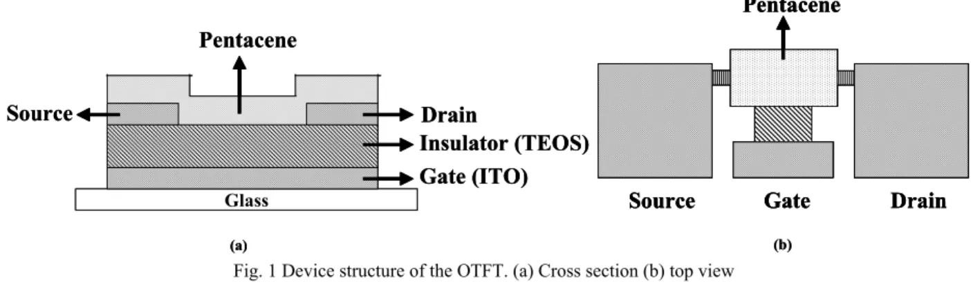
Fig. 1 shows the configuration of our OTFT device, we use a bottom gate and bottom contact structure. The electrodes, including source, drain, and gate are all made by indium-tin-oxide (ITO) with a thickness of 100 nm, which were deposited on a glass substrate by sputtering. The material of gate insulator is tetraethoxysilane(TEOS) with a thickness of 300 nm. It was prepared by plasma-enhanced chemical vapor deposition (PECVD). The channel lengths of the devices were 17, 27, 37, 47, and 57 µm, and the channel width were all 500 µm.
*[email protected]; phone 886 2 2363-5251 ext. 540; fax 886 2 2367-7467
Organic Field-Effect Transistors V, edited by Zhenan Bao, David J. Gundlach Proc. of SPIE Vol. 6336, 63361F, (2006) · 0277-786X/06/$15 · doi: 10.1117/12.678972
The substrate was first cleaned by supersonic bath with de-ionized water, acetone and methanol, each for 5 minutes. Then the substrate was baked at 130 oC for 20 minutes by a hot-plate and treated by oxygen plasma for 90 sec.
After all the pretreatment, the pentacene active layer was deposited by thermal evaporation with the deposition rate of 0.4 Å/sec and the thickness of 1000 Å through a steel shadow mask. Without heating the substrate, the temperature of the substrate was kept in room temperature and the pressure of the chamber was kept in high vacuum of 6*10-6 during
the evaporating. After the evaporation, an HP 4156C Precision Semiconductor Parameter Analyzer was used to measure the characteristic of the OTFTs. The OTFTs were all measured and stored under air environment.
Glass Pentacene Insulator (TEOS) Gate (ITO) Drain Source Pentacene Gate Drain Source (a) (b) Glass Pentacene Insulator (TEOS) Gate (ITO) Drain Source Pentacene Gate Drain Source Pentacene Gate Drain Source (a) (b)
Fig. 1 Device structure of the OTFT. (a) Cross section (b) top view
3. RESULTS AND DISCUSSIONS
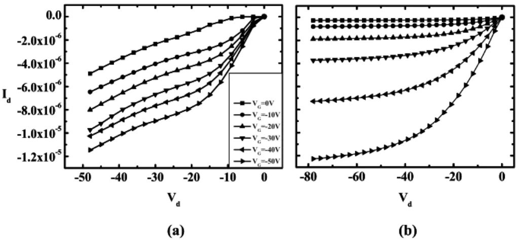
Fig. 2 (a) and (b) shows the ID-VDS curves for the OTFT without and with baking after the wet clean processes of a
channel length of 57 µm with varying VG values from 0, -10, -20, -30, -40 and -50 V, respectively. From Fig. 2(a), it can
be observed that the leakage current is very large when the substrate is not baked. On the other hand, after baking at 130 for 20 min (Fig. 2 (b)), we can see the leakage current has a dramatic decrease. Hence, we assume that the leakage current is attributed to the solvent which affect the carrier transfer in the channel or direct affect by the mobile ion from the solvent.
The mobility values of the OTFT can be deduced from the basic transistor equations
(
g t)
ds ds dark oxL
V
V
V
V
I
W
C
I
+
⎥⎦
⎤
⎢⎣
⎡
−
−
=
22
1
µ
(1)(
g t)
dark oxV
V
I
L
W
C
I
=
−
2+
2
1
µ
(2)Eq. 1 and 2 describe the I-V characteristics in the triode and saturation region, respectively. In these equations, W is the channel width, L is the channel length, µ is the mobility, Vt is the threshold voltage which can be obtained from the
curve of drain current versus gate voltage (Id-Vg), Cox is the capacitance per unit area of the insulating layer, and Idark is
the dark current or leakage current. From Fig. 2 (b), we can derive that the mobility value is 0.07 cm2/Vs in our devices
and the Id = 12 µA under the operation with Vg=-50 V and Vds=-80 V, which is quite high for the OTFTs fabrication
without heating the substrate. It may result from oxygen plasma treatment and/or other surface treatment before the evaporation.
-80 -60 -40 -20 0 Vd -50 -40 -30 -20 -10 0 -1.2x10⁻⁵ -1.0x10⁻⁵ -8.0x10⁻⁶ -6.0x10⁻⁶ -4.0x10⁻⁶ -2.0x10⁻⁶ 0.0 VG=0V VG=-10V VG=-20V VG=-30V VG=-40V VG=-50V Id Vd (a) (b) -80 -60 -40 -20 0 Vd -50 -40 -30 -20 -10 0 -1.2x10⁻⁵ -1.0x10⁻⁵ -8.0x10⁻⁶ -6.0x10⁻⁶ -4.0x10⁻⁶ -2.0x10⁻⁶ 0.0 VG=0V VG=-10V VG=-20V VG=-30V VG=-40V VG=-50V Id Vd (a) (b)
Fig. 2 Id-Vds curves of the OTFT. (a) Without baking the substrate before the evaporation. (b) The substrate was baked at 130 for
20 minutes before the evaporation.
Fig. 3 shows the Id-Vds curves for the OTFT measured at different storage time. During the storage, the OTFT are
put in the air environment and there is no passivation layer on the devices.
Compared the drain current value after 3 days and 12 days storage, the drain current of the OTFT with the channel length of 37 µm was slightly decreased from -0.63 µA to the value of -0.56 µA in 9 days, under the operation with Vg
=-50 V and Vds=-50 V. And for the device with the channel length of 57 µm, the drain current was decreased from -0.52
µA to the value of -0.44 µA. It shows the well air-stable properties for the magnitude of the drain current decreased less than 30% compared to the initial value after exposure in air for about 2 weeks.
-50 -40 -30 -20 -10 0 -7.0x10⁻⁷ -6.0x10⁻⁷ -5.0x10⁻⁷ -4.0x10⁻⁷ -3.0x10⁻⁷ -2.0x10⁻⁷ -1.0x10⁻⁷ 0.0 1.0x10⁻⁷ 2.0x10⁻⁷ VGS=0V VGS=-10V VGS=-20V VGS=-30V VGS=-40V VGS=-50V ID VDS -50 -40 -30 -20 -10 0 -6.0x10⁻⁷ -5.0x10⁻⁷ -4.0x10⁻⁷ -3.0x10⁻⁷ -2.0x10⁻⁷ -1.0x10⁻⁷ 0.0 1.0x10⁻⁷ 2.0x10⁻⁷ VGS=0V VGS=-10V VGS=-20V VGS=-30V VGS=-40V VGS=-50V ID VDS
L=37
L=57
3 days
-50 -40 -30 -20 -10 0 VG=0V VG=-10V VG=-20V VG=-30V VG=-40V VG=-50V VDS -50 -40 -30 -20 -10 0 VG=0V VG=-10V VG=-20V VG=-30V VG=-40V VG=-50V VDS8 days
-50 -40 -30 -20 -10 0 VG=0V VG=-10V VG=-20V VG=-30V VG=-40V VG=-50V VDS -50 -40 -30 -20 -10 0 VG=0V VG=-10V VG=-20V VG=-30V VG=-40V VG=-50V VDS12 days
-50 -40 -30 -20 -10 0 -7.0x10⁻⁷ -6.0x10⁻⁷ -5.0x10⁻⁷ -4.0x10⁻⁷ -3.0x10⁻⁷ -2.0x10⁻⁷ -1.0x10⁻⁷ 0.0 1.0x10⁻⁷ 2.0x10⁻⁷ VGS=0V VGS=-10V VGS=-20V VGS=-30V VGS=-40V VGS=-50V ID VDS -50 -40 -30 -20 -10 0 -6.0x10⁻⁷ -5.0x10⁻⁷ -4.0x10⁻⁷ -3.0x10⁻⁷ -2.0x10⁻⁷ -1.0x10⁻⁷ 0.0 1.0x10⁻⁷ 2.0x10⁻⁷ VGS=0V VGS=-10V VGS=-20V VGS=-30V VGS=-40V VGS=-50V ID VDSL=37
L=57
3 days
-50 -40 -30 -20 -10 0 VG=0V VG=-10V VG=-20V VG=-30V VG=-40V VG=-50V VDS -50 -40 -30 -20 -10 0 VG=0V VG=-10V VG=-20V VG=-30V VG=-40V VG=-50V VDS8 days
-50 -40 -30 -20 -10 0 VG=0V VG=-10V VG=-20V VG=-30V VG=-40V VG=-50V VDS -50 -40 -30 -20 -10 0 VG=0V VG=-10V VG=-20V VG=-30V VG=-40V VG=-50V VDS8 days
-50 -40 -30 -20 -10 0 VG=0V VG=-10V VG=-20V VG=-30V VG=-40V VG=-50V VDS -50 -40 -30 -20 -10 0 VG=0V VG=-10V VG=-20V VG=-30V VG=-40V VG=-50V VDS12 days
-50 -40 -30 -20 -10 0 VG=0V VG=-10V VG=-20V VG=-30V VG=-40V VG=-50V VDS -50 -40 -30 -20 -10 0 VG=0V VG=-10V VG=-20V VG=-30V VG=-40V VG=-50V VDS12 days
Fig. 3 Id-Vds curves of the OTFT with different storage time.
To discuss the behavior of the carrier accumulation in the channel under the bias stress, a DC bias stress experiment was conducted. Fig. 4 shows the drain current versus time with VDS=-35V, VG=-50V and the corresponding
ID-VDS curves of different stressing time. In Fig. 4(a), the current was increased dramatically from -0.39 µA to -1.8 µA
at the first 20 minutes and then was nearly maintained around -1.6 µA for the remaining 3 hours. The same behavior was also observed in the corresponding Id-Vds curves of different stressing time in Fig. 4(b), the drain current was
increased from -0.27 µA before the bias stress to -0.46 µA after 3 hours stressing operation, and recovered to -0.25 µA after the bias stress for 1 day. It shows a significant enhancement after the bias operation. In the case of largest enhancement, the later current was nearly 2 times of the original value and then recovered to almost the same value as the current before bias operation after removing the bias voltage. This current enhancement effect is reproducible. Once again we apply the bias, the current enhancement will be observed again. It indicates that the influences on the current caused by the voltage bias are reversible and reproducible. The origins of these effects may come from the non-uniformly accumulation of the carriers in the channel under the voltage bias [6].
0 30 60 90 120 150 180 -2.0x10⁻⁶ -1.8x10⁻⁶ -1.6x10⁻⁶ -1.4x10⁻⁶ -1.2x10⁻⁶ -1.0x10⁻⁶ -8.0x10⁻⁷ -6.0x10⁻⁷ -4.0x10⁻⁷ -2.0x10⁻⁷ ID Time (min) ID (a) 0 30 60 90 120 150 180 -2.0x10⁻⁶ -1.8x10⁻⁶ -1.6x10⁻⁶ -1.4x10⁻⁶ -1.2x10⁻⁶ -1.0x10⁻⁶ -8.0x10⁻⁷ -6.0x10⁻⁷ -4.0x10⁻⁷ -2.0x10⁻⁷ ID Time (min) ID (a) -50 -40 -30 -20 -10 0 -5.0x10⁻⁷ -4.5x10⁻⁷ -4.0x10⁻⁷ -3.5x10⁻⁷ -3.0x10⁻⁷ -2.5x10⁻⁷ -2.0x10⁻⁷ -1.5x10⁻⁷ -1.0x10⁻⁷ -5.0x100.0-8 5.0x10⁻⁸ VG=0V VG=-10V VG=-20V VG=-30V VG=-40V VG=-50V ID VDS -50 -40 -30 -20 -10 0 VG=0V VG=-10V VG=-20V VG=-30V VG=-40V VG=-50V VDS -50 -40 -30 -20 -10 0 VG=0V VG=-10V VG=-20V VG=-30V VG=-40V VG=-50V VDS
Before stress
Stress for 3 hours
1 day after stress for 10hr
(b) -50 -40 -30 -20 -10 0 -5.0x10⁻⁷ -4.5x10⁻⁷ -4.0x10⁻⁷ -3.5x10⁻⁷ -3.0x10⁻⁷ -2.5x10⁻⁷ -2.0x10⁻⁷ -1.5x10⁻⁷ -1.0x10⁻⁷ -5.0x100.0-8 5.0x10⁻⁸ VG=0V VG=-10V VG=-20V VG=-30V VG=-40V VG=-50V ID VDS -50 -40 -30 -20 -10 0 VG=0V VG=-10V VG=-20V VG=-30V VG=-40V VG=-50V VDS -50 -40 -30 -20 -10 0 VG=0V VG=-10V VG=-20V VG=-30V VG=-40V VG=-50V VDS
Before stress
Stress for 3 hours
1 day after stress for 10hr
-50 -40 -30 -20 -10 0 -5.0x10⁻⁷ -4.5x10⁻⁷ -4.0x10⁻⁷ -3.5x10⁻⁷ -3.0x10⁻⁷ -2.5x10⁻⁷ -2.0x10⁻⁷ -1.5x10⁻⁷ -1.0x10⁻⁷ -5.0x100.0-8 5.0x10⁻⁸ VG=0V VG=-10V VG=-20V VG=-30V VG=-40V VG=-50V ID VDS -50 -40 -30 -20 -10 0 VG=0V VG=-10V VG=-20V VG=-30V VG=-40V VG=-50V VDS -50 -40 -30 -20 -10 0 VG=0V VG=-10V VG=-20V VG=-30V VG=-40V VG=-50V VDS -50 -40 -30 -20 -10 0 -5.0x10⁻⁷ -4.5x10⁻⁷ -4.0x10⁻⁷ -3.5x10⁻⁷ -3.0x10⁻⁷ -2.5x10⁻⁷ -2.0x10⁻⁷ -1.5x10⁻⁷ -1.0x10⁻⁷ -5.0x100.0-8 5.0x10⁻⁸ VG=0V VG=-10V VG=-20V VG=-30V VG=-40V VG=-50V ID VDS -50 -40 -30 -20 -10 0 VG=0V VG=-10V VG=-20V VG=-30V VG=-40V VG=-50V VDS -50 -40 -30 -20 -10 0 VG=0V VG=-10V VG=-20V VG=-30V VG=-40V VG=-50V VDS
Before stress
Stress for 3 hours
1 day after stress for 10hr
(b)
Fig. 4 (a) ID versus time under DC stress. (b) Id-Vds curves of the corresponding stressing time.
Fig. 5 shows another result of the bias stress operation with Vds= -50V, Vg=-50V for 24 hours and the
corresponding Id-Vds curves after different stressing time. In this case, the current was increased from -11 µA to -13.4
µA during the first 10 minutes bias operation and was decreased to -3.6 µA in 24 hours. It shows the current was still increased under higher voltage bias, but it was decreased rapidly during the remaining operation. The same result can also be observed from the drain current values in the ID-VDS curves, under the operation with Vg=-50 V and Vds=-80 V,
the drain current value was increased from -14.1 µA to -20 µA and then was decreased to -0.78 µA. This result shows that the drain current under the bias stress is related to the operation voltage. If the bias voltage is too large, the performances of the OTFT will degrade quickly. But the drain current values will exhibit a significant enhancement if
we applied a proper bias voltage on the OTFT and the enhancement is reversible and reproducible. It shows the potential of being the memory device in the proper operation voltage based on this pentacene transistor [7].
0 5 10 15 20 -1.4x10⁻⁵ -1.3x10⁻⁵ -1.2x10⁻⁵ -1.1x10⁻⁵ -1.0x10⁻⁵ -9.0x10⁻⁶ -8.0x10⁻⁶ -7.0x10⁻⁶ -6.0x10⁻⁶ -5.0x10⁻⁶ -4.0x10⁻⁶ -3.0x10⁻⁶ ID Time (min) 0 167 333 500 667 833 Time (min) 0 167 333 500 667 833 Time (min) (a) 0 5 10 15 20 -1.4x10⁻⁵ -1.3x10⁻⁵ -1.2x10⁻⁵ -1.1x10⁻⁵ -1.0x10⁻⁵ -9.0x10⁻⁶ -8.0x10⁻⁶ -7.0x10⁻⁶ -6.0x10⁻⁶ -5.0x10⁻⁶ -4.0x10⁻⁶ -3.0x10⁻⁶ ID Time (min) 0 167 333 500 667 833 Time (min) 0 167 333 500 667 833 Time (min) 0 5 10 15 20 -1.4x10⁻⁵ -1.3x10⁻⁵ -1.2x10⁻⁵ -1.1x10⁻⁵ -1.0x10⁻⁵ -9.0x10⁻⁶ -8.0x10⁻⁶ -7.0x10⁻⁶ -6.0x10⁻⁶ -5.0x10⁻⁶ -4.0x10⁻⁶ -3.0x10⁻⁶ ID Time (min) 0 167 333 500 667 833 Time (min) 0 167 333 500 667 833 Time (min) (a) -80 -70 -60 -50 -40 -30 -20 -10 0 10 -2.2x10⁻⁵ -2.0x10⁻⁵ -1.8x10⁻⁵ -1.6x10⁻⁵ -1.4x10⁻⁵ -1.2x10⁻⁵ -1.0x10⁻⁵ -8.0x10⁻⁶ -6.0x10⁻⁶ -4.0x10⁻⁶ -2.0x100.0-6 2.0x10⁻⁶ 4.0x10⁻⁶ V G=0V V G=-10V V G=-20V V G=-30V VG=-40V VG=-50V ID VDS -80 -70 -60 -50 -40 -30 -20 -10 0 10 VG=0V VG=-10V V G=-20V V G=-30V V G=-40V VG=-50V VDS -80 -70 -60 -50 -40 -30 -20 -10 0 10 VG=0V VG=-10V VG=-20V VG=-30V VG=-40V V G=-50V VDS -80 -70 -60 -50 -40 -30 -20 -10 0 10 VG=0V V G=-10V VG=-20V VG=-30V VG=-40V VG=-50V VDS
Before Stress
20 min
12 hour
24 hour
(b) -80 -70 -60 -50 -40 -30 -20 -10 0 10 -2.2x10⁻⁵ -2.0x10⁻⁵ -1.8x10⁻⁵ -1.6x10⁻⁵ -1.4x10⁻⁵ -1.2x10⁻⁵ -1.0x10⁻⁵ -8.0x10⁻⁶ -6.0x10⁻⁶ -4.0x10⁻⁶ -2.0x100.0-6 2.0x10⁻⁶ 4.0x10⁻⁶ V G=0V V G=-10V V G=-20V V G=-30V VG=-40V VG=-50V ID VDS -80 -70 -60 -50 -40 -30 -20 -10 0 10 VG=0V VG=-10V V G=-20V V G=-30V V G=-40V VG=-50V VDS -80 -70 -60 -50 -40 -30 -20 -10 0 10 VG=0V VG=-10V VG=-20V VG=-30V VG=-40V V G=-50V VDS -80 -70 -60 -50 -40 -30 -20 -10 0 10 VG=0V V G=-10V VG=-20V VG=-30V VG=-40V VG=-50V VDS
Before Stress
20 min
12 hour
24 hour
-80 -70 -60 -50 -40 -30 -20 -10 0 10 -2.2x10⁻⁵ -2.0x10⁻⁵ -1.8x10⁻⁵ -1.6x10⁻⁵ -1.4x10⁻⁵ -1.2x10⁻⁵ -1.0x10⁻⁵ -8.0x10⁻⁶ -6.0x10⁻⁶ -4.0x10⁻⁶ -2.0x100.0-6 2.0x10⁻⁶ 4.0x10⁻⁶ V G=0V V G=-10V V G=-20V V G=-30V VG=-40V VG=-50V ID VDS -80 -70 -60 -50 -40 -30 -20 -10 0 10 VG=0V VG=-10V V G=-20V V G=-30V V G=-40V VG=-50V VDS -80 -70 -60 -50 -40 -30 -20 -10 0 10 VG=0V VG=-10V VG=-20V VG=-30V VG=-40V V G=-50V VDS -80 -70 -60 -50 -40 -30 -20 -10 0 10 VG=0V V G=-10V VG=-20V VG=-30V VG=-40V VG=-50V VDS
Before Stress
20 min
12 hour
24 hour
(b)
Fig. 5 (a) ID versus time under DC stress. (b) Id-Vds curves of the corresponding stressing time.
Fig. 6 shows the more complicated measurement of bias stress. The definition of source and drain electrodes were exchanged after the bias stress. Then after another bias stress, the source and drain electrodes were changed back to the origin and the bias was applied again. In each times of stressing, we repeat the Id-Vds measurements from 0 to -50 V
with the Vg values of 0, -10, -20, -30, -40, and -50 V for 10 minutes. In Fig. 6(b), the drain current was increased
obviously from -0.75 to -2.8 µA at Vg= -50V and Vds=-50V. When the source and drain were exchanged, the current
decreases to the 0.08 µA, nearly one tens of the original values, and it was almost recover back to the original values after another 10 minutes operation. It indicates that the holes were accumulated near the drain electrode after the bias stress, so the drain current was decreased significantly. Then after exchange the source and drain electrodes and applied the same bias operation, the carrier distribution was recovered to almost uniformly, result in the same current values as the original. In Fig. 6(e) and Fig. 6(f), the source and drain electrodes were change back to the origin and then another 10 minutes bias operation was applied, the increased of the drain current indicate that the operation is reproducible.
-50 -40 -30 -20 -10 0 VG=0V VG=-10V VG=-20V VG=-30V VG=-40V VG=-50V ID VDS -50 -40 -30 -20 -10 0 V G=0V VG=-10V VG=-20V V G=-30V VG=-40V VG=-50V ID VDS -50 -40 -30 -20 -10 0 -3.0x10⁻⁶ -2.5x10⁻⁶ -2.0x10⁻⁶ -1.5x10⁻⁶ -1.0x10⁻⁶ -5.0x10⁻⁷ 0.0 VG=0V VG=-10V VG=-20V VG=-30V VG=-40V VG=-50V ID VDS -50 -40 -30 -20 -10 0 -3.0x10⁻⁶ -2.5x10⁻⁶ -2.0x10⁻⁶ -1.5x10⁻⁶ -1.0x10⁻⁶ -5.0x10⁻⁷ 0.0 VG=0V VG=-10V VG=-20V VG=-30V VG=-40V VG=-50V VDS -50 -40 -30 -20 -10 0 VG=0V VG=-10V VG=-20V VG=-30V VG=-40V VG=-50V VDS -50 -40 -30 -20 -10 0 VG=0V VG=-10V VG=-20V VG=-30V VG=-40V VG=-50V VDS S-D S-D (Stress) D-S D-S (Stress) S-D S-D (Stress) (a) (b) (c) (d) (e) (f) -50 -40 -30 -20 -10 0 VG=0V VG=-10V VG=-20V VG=-30V VG=-40V VG=-50V ID VDS -50 -40 -30 -20 -10 0 V G=0V VG=-10V VG=-20V V G=-30V VG=-40V VG=-50V ID VDS -50 -40 -30 -20 -10 0 -3.0x10⁻⁶ -2.5x10⁻⁶ -2.0x10⁻⁶ -1.5x10⁻⁶ -1.0x10⁻⁶ -5.0x10⁻⁷ 0.0 VG=0V VG=-10V VG=-20V VG=-30V VG=-40V VG=-50V ID VDS -50 -40 -30 -20 -10 0 VG=0V VG=-10V VG=-20V VG=-30V VG=-40V VG=-50V ID VDS -50 -40 -30 -20 -10 0 V G=0V VG=-10V VG=-20V V G=-30V VG=-40V VG=-50V ID VDS -50 -40 -30 -20 -10 0 -3.0x10⁻⁶ -2.5x10⁻⁶ -2.0x10⁻⁶ -1.5x10⁻⁶ -1.0x10⁻⁶ -5.0x10⁻⁷ 0.0 VG=0V VG=-10V VG=-20V VG=-30V VG=-40V VG=-50V ID VDS -50 -40 -30 -20 -10 0 -3.0x10⁻⁶ -2.5x10⁻⁶ -2.0x10⁻⁶ -1.5x10⁻⁶ -1.0x10⁻⁶ -5.0x10⁻⁷ 0.0 VG=0V VG=-10V VG=-20V VG=-30V VG=-40V VG=-50V VDS -50 -40 -30 -20 -10 0 VG=0V VG=-10V VG=-20V VG=-30V VG=-40V VG=-50V VDS -50 -40 -30 -20 -10 0 VG=0V VG=-10V VG=-20V VG=-30V VG=-40V VG=-50V VDS S-D S-D (Stress) D-S D-S (Stress) S-D S-D (Stress) (a) (b) (c) (d) (e) (f)
Fig. 6 Id-Vds curves of the corresponding stressing time. (a) before stressing (b) stressing for 10 minutes (c)exchange the source and
drain electrodes (d)stressing for 10 minutes after exchange the source and drain electrodes (e) change back the source and drain electrodes (f) stressing for 10 minutes after change back the source and drain electrodes
4. SUMMARY
In summary, through the pretreatment of the surface, we have successfully fabricated the OTFT base on pentacene with high-mobility air-stable properties without heating the substrate during the evaporation. For the device with the channel length of 57 µm and the channel width of 500 µm, the mobility value was 0.07 cm2/Vs and the degradation of the drain
current was less than 30% after 12 days storage in the air environment. Besides, the increase of the drain current was observed after the bias stress. A 4 times increasing of the drain current values can be reached by repeating the Id-Vds
measurements from 0 to -50 V with the Vg values of 0, -10, -20, -30, -40, and -50 V for 10 minutes. This behavior is
reversible and reproducible. It shows the potential of being a memory device under the proper bias voltage.
ACKNOWLEDGMENTS
This work was financially supported by ERSO/ITRI.
REFERENCES
1. G. Horowitz, Adv. Mater. 10, 365 (1998).
2. I. Kymissis, C. D. Dimitrakopoulos, and S. Purushothaman, IEEE Trans. on electron devices 48, 1060 (2001). 3. C. D. Dimitrakopoulos, and P. R. L. Malenfant, Adv. Mater. 14, 99 (2002).
4. Y. W. Wang, H. L. Cheng, Y. K. Wang, T. H. Hu, J. C. Ho, C. C. Lee , T. F. Lei, and C. F. Yeh, Thin Solid Films
467, 215 (2004).
5. S. J. Zilker, C. Detcheverry, E. Cantatore, and D. M. de Leeuw, Appl. Phys. Lett. 79, 1124 (2001). 6. M. Koehler, I. Biaggio, Phys. Rev. B 70, 045314 (2004).
7. G. Velu, C. Legrand, O. Tharaud, A. Chapoton, D. Remiens, G. Horowitz, Appl. Phys. Lett.79, 659 (2001).