Innovative Plasma Alignment Method in Flexible Liquid
Crystal Display Films
Kang-Hung Liu,aChin-Yang Lee,bCheng-Ta Ho,cHorng-Long Cheng,c Shih-Ting Lin,c Huang-Chin Tang,b Chia-Wei Kuo,b Chi-Chang Liao,b Han-Ping D. Shieh,aand Wei-Yang Chouc,z
a
Department of Photonics and Institute of Electro-optical Engineering, Department of Photonics and Display Institute, National Chiao Tung University, Hsinchu 300, Taiwan
b
Industrial Technology Research Institute, Hsinchu 310, Taiwan c
Institute of Electro-optical Science and Engineering, Center for Micro/Nano Science and Technology, National Cheng Kung University, Tainan 701, Taiwan
Liquid crystals共LCs兲 in flexible cell were aligned on polyimide 共PI兲 surface treated by a paperlike plasma beam. The beam had energy of 450 eV and incident angle of 70° with respect to normal flexible indium-zinc oxide-coated substrate. The pretilt angle and anchoring energy of LCs on plasma-aligned PI surface were almost identical to the angle and energy of the rubbing PI. However, optical performance of the plasma-aligned cell was superior to the rubbing cell under various bending conditions. Furthermore, such noncontact alignment technology is suitable for large area and roll-to-roll fabrication of flexible LC films. © 2007 The Electrochemical Society. 关DOI: 10.1149/1.2760319兴 All rights reserved.
Manuscript submitted January 25, 2007; revised manuscript received June 25, 2007. Available electronically August 2, 2007.
Thinner and more flexible monitors with bendable frames could become popular in the next generation of flat-panel displays. Con-ventional displays are fairly rigid and therefore more susceptible to damage, while flexible displays are lighter and more durable, and thus have better mobility and longer life. Hence, a substrate of plastic-polymer films or other bendable materials can be used in-stead of glass to produce flexible monitors. However, flexible dis-plays first must overcome scientific, manufacturing, and cost-related obstacles to reach mass production.1-5
Conventional liquid crystal display共LCD兲 works well for rigid displays because the backlight and substrates remain constant, mak-ing it easier to apply color filters to create images. However, when displays are bent, the image quality is distorted, and thus researchers are facing challenges in creating flexible LCDs based on conven-tional technologies. Therefore, to make flexible displays, it is impor-tant to select the most appropriate polymer film materials and to develop more effective LC alignment technology.6-11 There are many drawbacks in the traditional rubbing technique for LC align-ment, such as sample contamination, static charge generation, or scratches. Photoalignment method has a problem with reliability, while ion-beam-alignment method has issues related to uniformity.6,7Moreover, standard LC alignment method, involving the baking process of a polyimide共PI兲 alignment layer at a tempera-ture over 120°C, is widely used today. In general, flexible-plastic substrates are required to be processed at ambient temperature to avoid substrate deformation during the fabrication of flexible dis-plays. It is still a challenge to achieve uniform alignment of the LC on plastic-flexible substrates at a low temperature. Existing reports state that alignment of LC materials is possible at a low temperature.8,9 However, reported methods are complicated and therefore not suitable for mass-production processes. The tempera-ture of manufacturing process depends on the substrate used and can be overcome by using polymer materials with high glass tempera-ture共Tg兲, i.e., polycarbonate 共PC兲. Recently, Kim et al. proposed the
process of aligning layerless flexible LC display fabricated at ambi-ent temperature using an imprinting process.10However, new tech-nologies offering simple and more effective alignment have to be developed for practical applications and to become suitable for in-line processes.
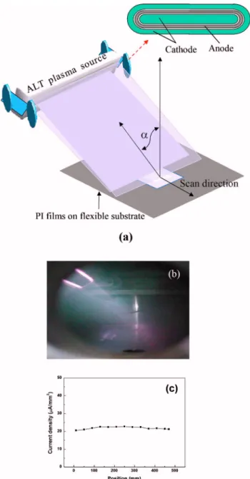
In this study, we propose a simple LC alignment technique that uses a paperlike plasma beam. The schematic diagram of the plasma aligned equipment is shown in Fig. 1a. The plasma source of this system contains inner and outer cathodes and anode, which define
the size and the shape of the discharge channel. The cathodes are grounded, while the anode is under positive potential. At the outer cathode, the source contains permanent magnets. The magnetic cir-cuit formed by steel body and cathodes is interrupted by the glow discharge gap. The plasma beam is formed in the crossed electric and magnetic fields within the discharge channel. The beam is used to treat PI surface and then to align LC on a flexible substrate. We have demonstrated that the technique is very effective to align most LCs, including bendable substrates. Compared with traditional rub-bing alignment, no damage from stresses or scratches on the surface of the flexible substrate was due to noncontact alignment originating from paperlike plasma beam. When the traditional rubbing process was performed on a flexible substrate under roll-to-roll fabrication, the sheer strain and deformation were induced by the roller. The rubbing depth was uncontrollable, resulting in nonuniform LC align-ment. Therefore, the plasma-alignment technique is also suitable for roll-to-roll fabrication of flexible LCDs. The substrates in our flex-ible microcell LCD films were made from 120m thick films of indium-zinc oxide共IZO兲-coated PC and were cleaned using alcohol. The LC layer with microcell structure was inserted between two plastic filmlike substrates. After microcell photospacers were formed, PI 共4170 R2, Nissan Chemical兲 alignment layers, with thickness of 80 nm, were printed using a conventional method. Crossed ultrathin polarizers covered the exterior sides of the plastic substrates. The total thickness of the microcell LCD film was about 520m.
To keep the cell gap constant under bending conditions, a photolithography-etching process with good repetition ratio was used to produce high-quality spacers of the microstructure. First, a 5m thick layer of positive photoresist 共PC403, JSR兲 was formed by spin-coating onto the IZO-coated PC substrate. Using a g-line stepper, striplike structures were patterned on the IZO substrate. Then, the striplike photospacers were baked at 180°C. The photo-spacer baking temperature was lower than the Tgtemperature of the PC substrate, which was equal to 220°C. Therefore, the baking pro-cess did not give rise to bending in the flexible substrate. The width and length of the spacer are 20 and 100m, respectively, with the same pitch of 260m, and the height of the spacer is kept at 5 m. The strip-shaped spacers used in the microcell arrays result in strong rigidity and make the LC-filling fabrication process easier. Thus, the alignment layers were printed on substrates followed by paperlike plasma treatment to achieve a homogeneous LC alignment. Follow-ing the printFollow-ing, the PI films were bombarded by a paperlike argon 共Ar兲 plasma beam with energy of 450 eV, which is the potential energy difference between the sample holder and accelerated elec-trode of the plasma beam. The base and working pressures are 0.01
z
E-mail: [email protected]
Electrochemical and Solid-State Letters, 10共10兲 J132-J135 共2007兲
1099-0062/2007/10共10兲/J132/4/$20.00 © The Electrochemical Society
J132
and 0.2 mTorr, respectively. The bombardment angle was 70° to the normal of the substrates and the bombardment procedure was re-peated ten times. The value of the size of the anode layer thruster 共ALT兲 is 480 ⫻ 90 mm, and the distance between the ALT and the substrate is 60 mm.12,13The moving speed of the sample holder was 6 mm/s. Figure 1b reveals that the flexible substrates were bom-barded by a paperlike plasma beam in a vacuum chamber. Compar-ing ion beam and paperlike plasma beam, the beam profile of ion beam is of Gaussian form; however, the plasma beam, which is like a sheet of paper in our case, has a uniform beam profile within the ALT source, as shown in Fig. 1c. Current density of the plasma beam is about 22A/mm2collected by a Faraday cup. A uniform
LC alignment occurred in the paperlike plasma beam alignment pro-cess, contrary to the ion beam alignment. The apparatus of plasma source was designed and fabricated by us. A successfully prior run had been achieved in the panel of LCD TV. We believe that such a
tool has potential for commercial fabrication of displays. Moreover, this plasma alignment method enables large-scale fabrication of flexible plastic substrates and has potential promising characteristics for industrial applications. After the lamination process, twist nem-atic 共TN兲 test panels were fabricated for electro-optical measure-ments. The positive-type LCs共MJ01744, Merck兲 were injected after the lamination process of the TN-mode test panel. Finally, two ul-trathin polarizers were laminated on the upper and lower plastic substrates to complete the test panel. For comparison purpose, the flexible LCD films were fabricated using conventional rubbing method. The subsequent fabrication processes for the rubbed flexible LCD films were the same as those used for plasma-aligned PI layers. Figure 2 shows the cell gap of flexible LCD films as a function of bending curvature for both LCD films with PI films produced by Ar plasma and conventional rubbing methods. The cell gap varia-tions of both LCD films are about 5% at the radii of the bending curvatures ranging from infinite, i.e., flat state, to 25 mm. The ob-tained result is an acceptable figure for flexible LCD films; there-fore, the cell gap of the LCD film can be well maintained by photo-spacers. Notably, the cell gaps of the LCD films, aligned by paperlike Ar plasma, are smaller 共0.1 m兲 than those aligned by rubbing due to the loss of photospacers during the alignment pro-cess. The pretilt angles of plasma and rubbing aligned LCD films are 2.33 and 2.25°, respectively, as measured by the autronic-MELCHERS GmbH TBA-107 measurement system. The pretilt angle of the LCD film aligned by paperlike Ar plasma is identical to the angle of the film aligned by rubbing for the same PI. Hence, the optimum paperlike plasma beam incidence angle and energy were suitable for fabrication of a flexible TN-mode LCD film. Moreover, plasma alignment could be applied in a roll-to-roll process.
To compare optical performance of plasma and rubbing aligned flexible films, the transmission vs applied voltage共V-T兲 curves were measured between 0 and 5 V using Otsuka LCD5100 at various bending curvatures, as shown in Fig. 3. As shown in Fig. 3a, the transmission characteristics of the flexible TN LCD film, produced by the paperlike plasma beam, are similar to the characteristics of the film with cells aligned by rubbing, which are shown in Fig. 3b. The threshold voltage of both flexible panels is almost the same at approximately 1.5 V. This result implies that the anchoring energy, arising from the paperlike plasma beam bombarded PI, was almost the same as the energy of rubbing PI. Excellent anchor energy pro-duced by paperlike Ar plasma beam is superior to that propro-duced by general Ar+ion beam. Visually, the difference between the two
pan-els can be seen in the anomalous decrease of bright states, ranging from 0 to 1 V. The decrease in bright states takes place in the rubbing-aligned TN flexible LCD film along with the increase in the bending curvature. The transmittance of the rubbing-aligned LCD film maximally decreases up to 10% when the radius of bending
Figure 1. 共Color online兲 共a兲 Schematic of the paperlike Ar plasma beam
alignment system. The incident angle of the beam is tilted from the normal of the flexible substrate. Inset represents an ALT plasma source.共b兲 Picture of paperlike plasma beam taken from a view port and the ALT mounted on a vacuum scanner.共c兲 Beam profile of plasma beam.
Figure 2. 共Color online兲 Cell gap of the plasma and rubbing-aligned LCD
films as a function of the radius of bending curvature.
J133
Electrochemical and Solid-State Letters, 10共10兲 J132-J135 共2007兲 J133
reduces from infinity to 25 mm. However, the transmittance of plasma-aligned LCD film remains almost the same, even though the flexible film bends at different curvatures. The optical performance of the flexible panel aligned by plasma remains constant under bend-ing conditions. The decrease in transmittance, related to the increase of the bending curvature for rubbed LCD film, occurred due to the unaligned region produced by rubbing in the microcell. The un-aligned regions were evidently larger in the rubbed LCD film than the regions in the films produced by paperlike Ar plasma. The un-aligned area could further enlarge under bending conditions, thus resulting in greater decrease of transmittance. Moreover, we can expect that the dark state of the rubbed LCD film will decrease with increase of the curvature in the flexible film due to the light leakage coming from the unaligned region. However, we should note that the level of the light leakage cannot be clearly observed in Fig. 3b.
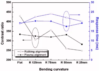
Finally, we investigated the response time and contrast ratio of experimental flexible LCD films fabricated using the paperlike Ar plasma beam and rubbing-aligned PI alignment layers. Response time is the amount of time in which a pixel in an LCD monitor takes to go from active 共white兲 to inactive 共black兲 and back to active 共white兲 again. It is measured in milliseconds 共ms兲. Lower numbers mean faster transitions and therefore fewer visible image artifacts. Response time共right axis兲 and contrast ratio 共left axis兲, as functions of the radius of bending curvature for both LCD films, are plotted in Fig. 4. The response time of both LCD films is almost the same. On average the response time was about 20 ms. Generally, the response time decreases along with decrease of the cell gap in LCDs. Figure 4 reveals that the response time of plasma-aligned LCD film slightly decreases with the increase of the bending curvature due to slight decrease in cell gap under bending conditions共see Fig. 2兲. However,
the response time of the rubbed LCD film initially increases and then decreases along with the increase of the bending curvature. This phenomenon was due to disordered LC molecules, which in-crease the response time, within the unaligned region on PI film. LC molecules are poorly aligned within the unaligned region which is near the photospacer and is enlarged under bending state. Generally, the response time of an LC cell decreases with decreasing cell gap of the LC cell. The cell gaps of both plasma and rubbing-aligned LCD films decrease as increasing the bending level of flexible sub-strates, as shown in Fig. 2. For plasma-aligned LCD film, there is a tendency toward the response time decreasing with decreasing cell gap, as shown in Fig. 4. However, there is an effect of disordered LC molecules within the unaligned region on PI film near the spacer for rubbed LCD film besides the effect of cell gap. The unaligned region will be enlarged under bending state to result in increasing the response time further. Therefore, the response time for rubbed LCD film has a peak. The response time values obtained for experi-mental LCD films are more than adequate for LCDs with cell gap of 5m. The contrast ratio of the flexible LCD film with a plasma-aligned PI layer was about 330. The film exhibited variation equal to approximately 15% at the radius of bending curvature ranging from infinity to 25 mm. The contrast ratio of the rubbed LCD film de-creased greatly when bending curvature inde-creased. The variation of the contrast ratio for rubbed flexible film reaches up to 42%. Ob-tained results indicate that the alignment uniformity of the film pro-duced by paperlike Ar plasma method is much better than the uni-formity of the film produced by rubbing technique under bending condition. Additionally, the uniformity of contrast ratio for plasma and rubbing-aligned LCDs is 330 ± 9.1 and 430 ± 41.4, respec-tively, measured at 13 positions on flat panels. These results reveal that the uniformity of LC alignment through plasma beam method is better than that through traditional rubbing method. The conclusion is also consistent with V-T measurements. Furthermore, the surfaces of paperlike plasma beam and rubbing-aligned PI were observed by polarized optical microscope using 50⫻ objective lens. When the black images 共Fig. 5a and c兲 were taken from the optical micro-scope, two polarizers were parallel to each other, as shown in Fig. 5e, due to the TN mode of the LCD under zero applied voltage. Contrary to black images, the white images共Fig. 5b and d兲 were recorded under a pair of perpendicular polarizers, as shown in Fig. 5f. The irradiation of plasma beam for both glass substrates is like the polarization directions of the microscope in Fig. 5f. Moreover, the alignment direction of LC is the same as the irradiation direction of plasma beam. Figures 5a and b reveal that there are defects in-cluding contamination and scratches on the rubbed PI surface;
how-Figure 3. 共Color online兲 Transmission vs applied voltage curves for 共a兲 a
flexible cell aligned by plasma-beam-processed PI at angle of 70° to the normal of substrate and共b兲 a flexible test cell aligned by traditional rubbing PI under various bending curvatures.
Figure 4. 共Color online兲 Contrast ratio 共left axis兲 and response time 共right
axis兲 as a function of radius of bending curvature for plasma and rubbing-aligned LCD films.
J134 Electrochemical and Solid-State Letters, 10共10兲 J132-J135 共2007兲
J134
ever, plasma-beam-alignment PI surface has perfect morphology like native PI film, as shown in Fig. 5c and d. We are currently working on improving optical characteristics of the flexible LCD aligned by plasma alignment technology presented in our article.
In summary, we have used a paperlike plasma-beam-irradiated PI film to produce an alignment layer suitable for flexible LCD manu-facturing. The level of the anchoring energy for noncontact plasma-aligned LCD was the same as the energy level of a rubbed panel. In
terms of optical performance under bending conditions, the flexible LCD film aligned by plasma method was superior to the rubbed LCD film. Furthermore, by extending the anode layer thruster plasma source, we found that the paperlike plasma is suitable for larger area panel and roll-to-roll production. A study on the atmo-spheric pressure plasma is in progress in order to address the vacuum issues.
Acknowledgment
The authors thank the National Science Council of Taiwan for financially supporting this research under contract no. NSC 95-2112-M-006-005 and NSC 95-2221-E-006-430.
Industrial Technology Research Institute assisted in meeting the publica-tion costs of this article.
References
1. S. C. Jeng, K. H. Chang, J. M. Ding, L. P. Hsin, C. Y. Lin, Y. R. Lin, K. H. Liu, C. C. Lu, Y. A. Sha, H. L. Wang, and C. C. Liao, J. Soc. Inf. Disp., 13, 475共2005兲. 2. S. R. Forrest, Nature (London), 428, 911共2004兲.
3. Y. Chen, J. Au, P. Kazlas, A. Ritenour, H. Gates, and M. McCreary, Nature (Lon-don), 423, 136共2003兲.
4. I. Shiyanovskaya, A. Khan, S. Green, G. Magyar, and J. W. Doane, SID Interna-tional Symposium Digest Tech. Papers, 36, 1556共2005兲.
5. D.-W. Kim, C.-J. Yu, Y.-W. Lim, J.-H. Na, and S.-D. Lee, Appl. Phys. Lett., 87, 051917共2005兲.
6. W. Y. Chou and H. L. Cheng, Adv. Funct. Mater., 14, 811共2004兲, and references therein.
7. W. Y. Chou, Z. Y. Ho, F. C. Tang, Y. S. Mai, T. Y. Wu, H. L. Cheng, C. R. Sheu, C. C. Liao, and K. H. Liu, Jpn. J. Appl. Phys., Part 2, 44, L876共2005兲. 8. S.-J. Kim, T. Ahn, M. C. Suh, C.-J. Yu, D.-W. Kim, and S.-D. Lee, Jpn. J. Appl.
Phys., Part 2, 44, L1109共2005兲.
9. A. Rastegar, M. Skarabot, B. Blij, and Th. Rasing, J. Appl. Phys., 89, 960共2001兲. 10. Y. T. Kim, S. Hwang, J. H. Hong, and S. D. Lee, Appl. Phys. Lett., 89, 173506
共2006兲.
11. J.-H. Kim, M. Yoneya, and H. Yokoyama, Nature (London), 420, 159共2002兲. 12. K.-Y. Wu, P.-C. Liu, C.-Y. Lee, C.-H. Chen, H.-K. Wei, C.-M. Yeh, C.-S. Kou, and
J. Hwang, J. Appl. Phys., 98, 083518共2005兲.
13. K.-Y. Wu, C.-Y. Lee, S.-J. Chang, J. Hwang, H.-C. Tang, C.-W. Chen, C.-D. Lee, and C.-H. Liu, J. Appl. Phys., 101, 023531共2007兲.
Figure 5.共Color online兲 Black and white polarized optical microscope
im-ages of共a兲 and 共b兲 rubbed PI surface, 共c兲 and 共d兲 plasma-aligned PI surface, and共e兲 and 共f兲 a pair of parallel and perpendicular polarizers of the optical microscope, respectively. The size of images is 10⫻ 6 mm.
J135
Electrochemical and Solid-State Letters, 10共10兲 J132-J135 共2007兲 J135