Jiin-Long Yang and J.S. Chena)
Department of Materials Science and Engineering, National Cheng Kung University, Tainan 70101, Taiwan, Republic of China
S.J. Chang
Department of Electrical Engineering, Institute of Microelectronics, National Cheng Kung University, Tainan 70101, Taiwan, Republic of China
(Received 16 June 2004; accepted 5 November 2004)
The distribution of Au and NiO in NiO/Au ohmic contact on p-type GaN was investigated in this work. Au (5 nm) films were deposited on p-GaN substrates by magnetron sputtering. Some of the Au films were preheated in N2ambient to agglomerate into semi-connected structure (abbreviated by agg-Au); others were not preheated and remained the continuous (abbreviated by cont-Au). A NiO film (5 nm) was deposited on both types of samples, and all samples were subsequently annealed in N2ambient at the temperatures ranging from 100 to 500 °C. The surface
morphology, phases, and cross-sectional microstructure were investigated by scanning electron microscopy, glancing incident angle x-ray diffraction, and transmission electron microscopy. I-V measurement on the contacts indicates that only the 400 °C annealed NiO/cont-Au/p-GaN sample exhibits ohmic behavior and its specific contact resistance (c) is 8.93 × 10
−3⍀ cm2
. After annealing, Au and NiO contact to GaN individually in the NiO/agg-Au/p-GaN system while the Au and NiO layers become tangled in the NiO/cont-Au/p-GaN system. As a result, the highly tangled NiO-Au structure shall be the key to achieve the ohmic behavior for NiO/cont-Au/p-GaN system.
I. INTRODUCTION
GaN is a semiconductor that has been extensively in-vestigated for optoelectronic applications,1,2such as light emitting diodes (LEDs) and laser diodes (LDs), because of its wide-spectrum and short-wavelength light emis-sion. The optoelectronic performance of GaN depends on not only the quality of GaN crystals but also the specific contact resistance of metal electrodes to n- and p-type GaN. However, it is a great challenge to obtain low con-tact resistance to p-type GaN because the carrier concen-tration of p-GaN cannot reach the degenerated level and lack of metals with high work function compared to the band gap of GaN. Thus, metallic materials with high work function are expected to alleviate the resistance. Multilayer metallizations with high work function, in-cluding Ni/Au,3–7Pt/Au,8Pt/Ru,9and Pd/Ru,10etc., have been widely fabricated as a contact to p-type GaN.
Many authors7,11–14 have reported that Au/Ni based bi-layer structure annealed in oxygen ambient or air is
able to form ohmic contacts to p-GaN with a specific contact resistance in the range of 10−2
to 10−6 ⍀ cm2 . The exact mechanism on the formation of ohmic con-tact to p-type GaN is still unclear and controversial. Ho et al.12fabricated Au/Ni/p-GaN contact structure and an-nealed the contacts in air. The final contact structure after annealing is Au/p-NiO/p-GaN. According to the equilib-rium energy-band diagram shown in that paper, p-type NiO forms Schottky barriers to both Au and p-type GaN. When the NiO is sufficiently thin (less than the depletion width), the carriers can tunnel through energy barriers in the Au/p-NiO/p-GaN hetero-junction structure. Hence, low resistance of ohmic contacts is obtained. Another mechanism proposed by Koide et al.14 suggests that the ohmic behavior is originated from the increasing hole concentration in the near surface region of p-GaN. The hole concentration is increased by removal of hydrogen atoms in GaN when the samples were annealed in the ambient containing oxygen.
The importance of Au layer and NiO in the contact was also discussed by Narayan et al.,15 who deposited Au/Ni/Au on p-type GaN. They stated that the first Au layer provides a template for NiO growth because of their a)
Address all correspondence to this author. e-mail: [email protected] DOI: 10.1557/JMR.2005.0066
of oxidizing Ni. Furthermore, the dissimilar distribution of Au and NiO in the contact was fabricated intentionally by heat treatment to investigate its effect on ohmic con-tact formation.
II. EXPERIMENTAL
The 4-m-thick undoped wurtzite GaN and 2.2-m-thick Mg doped GaN films were grown sequentially by metalorganic chemical vapor deposition (MOCVD) with carrier gas of hydrogen on (0001)-oriented sapphire sub-strate. Trimethylgallium and ammonia were used as the source reactants and bis-cyclopentadienyl-magnesium applied as the p-type dopant source.
The hole carrier concentration of Mg doped GaN was 1.29 × 1017cm−3
after annealing at 720 °C in N2 atmos-phere for 20 min. Before the deposition of the contact layers, the samples were immersed into 5.86 wt% KOH solution16,17
to remove the native oxide of the GaN sur-face and then rinsed in running deionized water. The 5-nm-thick Au films were then deposited by magnetron sputtering. Afterward, these samples were divided into two groups. Some of them were preheated in N2ambient at 200 °C for 5 min to agglomerate Au layer into semi-connected structure (agg-Au); however, others were omitted this procedure and maintained the continuous Au layer (cont-Au). Next, the NiO (5 nm) layer was sput-tered on both agg-Au and cont-Au samples with atmos-phere of 50% Ar and 50% O2. Recently, the effect of inductively coupled plasma (ICP)-induced damage to n-type GaN was studied by Choi et al.18–20 They have shown that significant plasma damage is seen at ICP power of 200 W or higher. In our reactive magnetron sputtering, the radio frequency (rf) power was applied as low as 30 and 100 W for Au and NiO deposition, respectively. The plasma damage induced by direct sputtering should be relatively small to harm the p-GaN substrate.
The metallized samples were heat treated by a furnace with N2 flow at 100, 200, 300, 400, and 500 °C for 10 min. The purity of the nitrogen gas used for annealing is 99.95%, which implies that some impurities such as O2
electron microscopy (SEM; Philips XL40 FE-SEM, Am-sterdam, The Netherlands).
The phases present in the contact metallization layers were characterized by glancing incident angle x-ray diffraction (Rigaku DMAX 2500, Japan) with an incident angle of 2°. The cross-sectional microstructure of NiO/ agg-Au/p-GaN and NiO/cont-Au/p-GaN samples was in-vestigated by transmission electron microscopy (TEM; Hitachi FE-2000, Japan). Besides, the carrier concentra-tion and resistivity of NiO films were measured based on the Hall-effect principle, by using van der Pauw’s method.23
III. RESULTS AND DISCUSSION
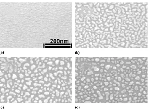
Fig. 1 presents the morphology of Au (5 nm) films after annealing at various temperatures. The as-deposited Au film was a smooth and continuous film [Fig. 1(a)] and it broke into a wormlike structure after annealing at 200 °C for 5 min [Fig. 1(b)]. Upon annealing at 250 and 300 °C, the Au film was agglomerated into islands, and became completely discontinuous [Figs. 1(c) and 1(d)]. It is apparent that the higher annealing temperature, the more agglomeration of Au films. The resistivity of agg-Au after annealing is worth understanding since it shall relate with the interconnectivity of the Au layer. How-ever, we cannot measure it by using four-point-probe method because the sheet resistance of the ultrathin (5 nm) Au film is intrinsically high and the loading of probes may destroy the Au film. For Au/Ni based con-tact, the TEM images show that Au film will agglomerate into individual Au islands and contact directly on p-GaN after annealing. The individual Au islands are a cross-sectional view of the Au network that lead to the low specific contact resistance.24 The wormlike structure of Fig. 1(b) is similar to the Au network because it shows agglomerated and semi-connected films. However, Figs. 1(c) and 1(d) reveal isolated Au islands, which cannot carry the current anymore because of interrupted electron transportation. Therefore, 200 °C was chosen as the preheating temperature for the agglomerated Au (agg-Au) layer.
NiO films of 5 nm in thickness were then deposited on the Au films with or without preheating. Figure 2(a) presents the SEM micrographs on the surfaces of NiO/agg-Au/p-GaN samples before and after annealing. It reveals that the agg-Au layer hardly changed its mor-phology after annealing up to 500 °C, implying that the top NiO layer will prevent the agg-Au film from further deformation. In contrast, Fig. 2(b) shows the SEM micro-graphs of NiO/cont-Au/p-GaN samples before and after annealing. Although the Au layer in this system is cov-ered with a NiO layer, it also agglomerates upon anneal-ing at 400 °C or lower, but in a less extent than the bare Au films (Fig. 1). The Au layer breaks but still remains continuous after annealing at 400 °C. However, after annealing at 500 °C, the surface of NiO/cont-Au/p-GaN is completely deteriorated and the Au layer has aggregated into large grains (average size of 150 nm in diameter).
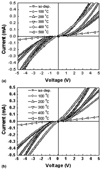
The I-V curves of NiO/agg-Au and NiO/cont-Au con-tacts on p-GaN, using CTLM structure, are shown in Fig. 3. These curves are obtained form the CTLM pat-terns with the spacing gap of 45 m. All NiO/agg-Au/p-GaN samples exhibit nonlinear I-V characteristics [Fig. 3(a)], indicating that the NiO/agg-Au contacts on p-GaN are rectifying. The I-V curve for 500 °C-annealed sample shows nearly linear in the range of −5 to 5 V. However, it cannot be judged as ohmic behavior because it becomes nonlinear over this voltage range. On the other hand, the I-V curves of NiO/cont-Au contacts on p-GaN [Fig. 3(b)] display nonlinear (as-deposited to 300 °C-annealed) or quasi-linear (400 and 500 °C an-nealed) characteristics. Again, the I-V curve of the
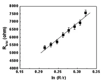
500 °C annealed sample is nearly linear, but it cannot be considered as ohmic behavior owing to the nonlinearity beyond the −5 to 5 V range. The I-V curve of the 400 °C annealed sample also shows almost, but not perfectly, linear characteristic. The slope of the curve varies from 1.40 × 10⁻⁴to 1.45 × 10⁻⁴, depending on the positions. To determine the c value of the 400 °C annealed NiO/cont-Au contact, the data of total resistance (Rtotal) obtained from I-V measurement was plotted as a function of ln(R/r), where R and r represent the radii of the outer and inner rings of CTLM structure, respectively, as shown in Fig. 4. As mentioned previously, the I-V curve of the 400 °C annealed sample is not perfectly linear. The slight variation in the slope of the I-V curve leads to an error in Rtotal. This error is indicated in Fig. 4 by the error bars. According to the CTLM theory, the total resistance follows the equation: Rtotal⳱ Rsh/2[ln(R/r) + Lt(1/R + 1/r)].21,22 The solid line shown in Fig. 4 is obtained by linear regression. Therefore, the sheet resistance of p-GaN (Rsh) and the transfer length (Lt) values can be derived from the slope and the intersect of the solid line in Fig. 4, and the values are 1.27 × 10⁵⍀/sq and 2.65 × 10⁻⁴cm, respectively. Finally, the specific contact resis-tance (c) was obtained as 8.93 × 10
−3 ⍀ cm2 by the equation ofc ⳱ Rsh× Lt.
21,22
Besides, in Fig. 3, there is no systematic dependence of current at a specific voltage versus the sample anneal-ing temperature. As we know, the electrical performance of microelectronic devices is sensitive to the character-istics of materials (e.g., resistivity, defects, phases, mi-crostructure, etc.), and interaction at interfaces (in the current study: NiO/Au, Au/p-GaN, and NiO/p-GaN). FIG. 1. SEM images on the surface of Au (5 nm)/p-GaN samples (a) as-deposited, and after annealing at (b) 200 °C, (c) 250 °C, and (d) 300 °C in N2ambient for 5 min.
Upon annealing, some “opposite” properties may occur simultaneously. For example, the crystallinity for both Au and NiO layers is improved after annealing because of the sharpening of x-ray diffraction peaks (will be shown in Fig. 7). The resistivity of Au will decrease with the increasing crystallinity; however, the resistivity of NiO will increase with the increasing crystallinity (will be shown later. The two contradictory but simultaneously occurring effects will lead to the complex result for the overall performance of the contact system, which may contribute to the lack of trend for the I-V curves.
To explore the mechanism for the formation of ohmic contacts, the cross section of NiO/agg-Au/p-GaN and NiO/cont-Au/p-GaN samples were examined by trans-mission electron microscopy. Figure 5(a) presents the cross-sectional image of NiO/agg-Au/p-GaN sample without postannealing, revealing that the height of agg-Au is around 20 nm and NiO layer covers on agg-agg-Au FIG. 2. SEM images on the surface of (a) NiO (5 nm)/agg-Au/p-GaN
and (b) NiO (5 nm) /cont-Au/p-GaN samples before and after anneal-ing at various temperatures in N2ambient for 10 min.
FIG. 3. I-V curves of (a) NiO (5 nm)/agg-Au/p-GaN and (b) NiO (5 nm)/cont-Au/ p-GaN samples, before and after annealing at various temperatures in N2 ambient. These curves are obtained from the CTLM patterns with the spacing gap of 45m.
uniformly. The Au islands cover partial area of the p-GaN surface, and the NiO layer contacts with the rem-nant p-GaN surface directly. The cross-sectional TEM image of NiO/agg-Au/p-GaN sample after annealing at 400 °C is displayed in Fig. 5(b), showing the structure of NiO/agg-Au/p-GaN sample hardly changes from that of as-deposited one. This result is consistent with the ob-servation of SEM [Fig. 2(a)], indicating that the NiO layer can keep agg-Au from further agglomeration dur-ing annealdur-ing.
Figure 6 presents the cross-sectional morphology of the NiO/cont-Au system and it is clearly distinct from that of the NiO/agg-Au system. The as-deposited NiO/cont-Au/p-GaN sample exhibits a uniform NiO/Au bilayer structure and there is no obvious inter-diffusion between the two layers [Fig. 6(a)]. After annealing at 400 °C, NiO and Au layers significantly diffuse to each other and forms a tangled structure [Fig. 6(b)]. The in-termixing of Au and NiO leads to a Au-NiO composite layer which covers the GaN substrate. However, the Au-to-GaN contacting area is larger than that of the annealed NiO/agg-Au/GaN system [Fig. 5(b)] because here the Au layer is less agglomerated.
To understand whether new phases have formed upon heat treatment, the crystal structure of NiO/cont-Au/p-GaN samples, before and after annealing, were examined by using GIA-XRD and the result is shown in Fig. 7. The GIA-XRD patterns indicate that no new phase has been produced upon annealing. The only change is the im-provement of crystallinity for both Au and NiO layers because of the sharpening of diffraction peaks after annealing.
According to the report by Ho et al.,12 formation of Au/Ni ohmic contact to p-GaN is attributed to the oxi-dation of Ni to NiO. The authors conjectured that NiO performs as a p-type semiconductor. When the NiO is
sufficiently thin (less than the depletion width), the car-riers can tunnel through energy barcar-riers in the Au/p-NiO/ p-GaN hetero-junction structure. We have characterized the carrier type of our sputtered NiO films by Hall meas-urement and it is proven to be p-type. Figure 8 shows the carrier concentration and resistivity of NiO films, as de-posited and after annealing at various temperatures. The as-deposited NiO shows hole carrier concentration and resistivity of 2.68 × 1021 cm−3and 2.98 × 10⁻¹ ⍀ cm, respectively. After annealing, both values decrease sig-nificantly. The carrier concentration diminishes to 1.03 × 10¹⁵
cm−3
when annealing at 400 °C; however, the NiO FIG. 4. Total resistance, obtained from linear I-V curves of the 400 °C
annealed NiO (5 nm)/cont-Au/p-GaN sample, as a function of ln(R/r) values.
FIG. 5. Cross-sectional TEM micrographs of NiO (5 nm)/agg-Au/p-GaN sample: (a) as-deposited and (b) after annealing at 400 °C in N2 ambient for 10 min.
film still preserves its p-type character. According to cross-sectional TEM images (Figs. 5 and 6), both NiO/ agg-GaN and NiO/cont-GaN form the Au/p-NiO/p-GaN structure after annealing at 400 °C. Never-theless, only the NiO/cont-Au system exhibits ohmic be-havior. Therefore, formation of p-NiO is not the only critical issue to obtain the ohmic contact on p-GaN.
In their sample with the lowest contact resistance, Ho et al.12observed agglomerated Au islands with undercut edges (contact angle of 120–140°), which is very similar to the feature of our 400 °C annealed NiO/agg-Au/p-GaN sample [Fig. 5(b)]. They suggested that the ultra-thin p-NiO layer filling in the undercut space would pro-vide the Au/thin p-NiO/p-GaN hetero-junction structure.
We support the presumption that formation of Au/thin p-NiO/p-GaN hetero-junction is the mechanism for achieving ohmic contacts. However, the present study demonstrates that the distribution of Au is also crucial for the formation of ohmic contacts. In the NiO/cont-Au/p-GaN system, the cont-Au layer tends to agglomerate upon annealing, which induces the intermixing of NiO/ cont-Au bilayer. The intermixing results in the direct contact of p-NiO to p-GaN, as well as the tangled distri-bution of Au [Fig. 6(b)]. Once the Au layer agglomerates to distinct islands, for example, the NiO/agg-Au system [Figs. 2(a) and 5] or the 500 °C annealed NiO/cont-Au sample [Fig. 2(b)], no ohmic character can be observed, in spite of the presence of Au/p-NiO/p-GaN junctions. Therefore, the tangled Au structure imparts a good net-work to the conduction of electrical current among the Au/p-NiO/p-GaN hetero-junctions, which is appar-ently a crucial aspect for the formation of ohmic contact on p-GaN.
FIG. 6. Cross-sectional TEM micrographs of NiO (5 nm)/cont-Au/p-GaN sample: (a) as-deposited and (b) after annealing at 400 °C in N2 ambient for 10 min.
FIG. 7. GIA-XRD patterns of NiO (5 nm)/cont-Au/p-GaN samples, before and after annealing at various temperatures in N2ambient.
FIG. 8. Carrier concentration and resistivity of sputtered NiO films (90 nm) deposited on glass, before and after annealing at various temperatures.
Additionally, Jang et al.25 reported that annealing Au/Ni/p-GaN under O2ambient would cause the prefer-ential outdiffusion of Ni to the contact surface to form NiO, leading to the final contact structure of NiO/Au/p-GaN. Ga atoms were dissolved in the Au contact layer and the oxygen atoms incorporated during annealing pro-moted the outdiffusion of Ga atoms from the GaN layer, leaving Ga vacancies below the contact. According to defect chemistry, existence of Ga vacancies will increase the carrier concentration for p-GaN. Consequently, the contact resistivity is reduced.
Due to the limitation of our analytical tools, we cannot identify Ga vacancies in p-GaN, and it is also difficult to quantify the dissolution of Ga in Au because the Au layer is very thin and it is right next to the GaN substrate. Nevertheless, it is very likely that there exists a higher amount of Ga dissolution in cont-Au than that in agg-Au, because the cont-Au sample has a greater Au-to-GaN contacting area than the agg-Au sample does (Figs. 5 and 6). Therefore, in addition to enhanced conductivity due to the tangled Au structure, the cont-Au contact may also dissolve Ga more efficiently and consequently improve the contact ohmicity.
IV. CONCLUSION
The importance of the Au distribution in the sputtered p-NiO/Au contact to the formation of ohmic contacts on p-type GaN is investigated. Intermixing of NiO/cont-Au bilayer upon annealing brings the direct contact between p-NiO and p-GaN, as well as the tangled distribution of Au. The tangled structure provides a good network to conduct the electrical current among the Au/p-NiO/p-GaN heterojunctions, while the large Au-to-Au/p-NiO/p-GaN contact-ing area for the cont-Au contact may also increase the dissolution of Ga in Au and improve the contact ohmic-ity. As a consequence, the conductivity of the whole contact is enhanced and the contact exhibits the ohmic characteristics. If the Au layer agglomerates to distinct islands during heat treatment, the contact will not be ohmic. Therefore, distribution of Au in the Au–NiO sys-tem can be a critical feature for the formation of ohmic contacts on p-GaN.
ACKNOWLEDGMENTS
The authors gratefully acknowledge the financial sup-port from the National Science Council of Taiwan, Re-public of China (Grant No. 90-2216-E-006-069). The authors also thank the support of the field emission gun-transmission electron microscope (FEG-TEM) facility at National Taiwan University.
REFERENCES
1. S. Nakamura, T. Mukai, and M. Senoh: High-brightness InGaN/ AlGaN double-heterostructure blue-green-light-emitting diodes.
J. Appl. Phys. 76, 8189 (1994).
2. S. Nakamura, M. Senoh, S. Nagahama, N. Iwasa, T. Yamada, T. Matsushita, Y. Sugimoto, and H. Kiyoku: High-power, long-lifetime InGaN multi-quantum- well-structure laser diodes. Jpn. J.
Appl. Phys. Part 2 36, L1059 (1997).
3. G. Mohs, B. Fluegel, H. Giessen, H. Tajalli, and N. Peyghambarian: Photoluminescence decay dynamics in an InGaN/AlGaN/GaN double- heterostructure. Appl. Phys. Lett. 67, 1515 (1995). 4. S. Nakamura, M. Senoh, S. Nagaham, N. Iwasa, T. Matsushuta,
H. Kiyiku, and Y. Sugimoto: Characteristics of InGaN multi-quantum-well-structure laser diodes. Appl. Phys. Lett. 68, 3269 (1996).
5. H. Ishikawa, S. Kobayashi, Y. Koide, S. Yamasaki, S. Nagai, J. Umezaki, M. Koike, and M. Murakami: Effects of surface treat-ments and metal work functions on electrical properties at p-GaN/ metal interfaces. J. Appl. Phys. 81, 1315 (1997).
6. J.K. Sheu, Y.K. Su, G.C. Chi, W.C. Chen, C.Y. Chen, C.N. Huang, J.M. Hong, Y.C. Yu, C.W. Wang, and E.K. Lin: The effect of thermal annealing on the Ni/Au contact of p-type GaN.
J. Appl. Phys. 83, 3172 (1998).
7. J-K. Ho, C-S. Jong, C-N. Huang, C-Y. Chen, C.C. Chiu, and K-K. Shih: Low-resistance ohmic contacts to p-type GaN. Appl.
Phys. Lett. 74, 1275 (1999).
8. D.J. King, L. Zhang, J.C. Ramer, S.D. Hersee, and L.F. Lester: Temperature behavior of Pt/Au ohmic contacts to p-GaN, in
Gal-lium Nitride and Related Materials II, edited by C.R. Abernathy,
H. Amano, and J.C. Zolper (Mater. Res. Soc. Symp. Proc. 468, Pittsburgh, PA, 1997), p. 421.
9. J.S. Jang, S.J. Park, and T.Y. Seong: Low resistance and thermally stable Pt/Ru ohmic contacts to p-type GaN. Phys. Status Solidi A 180,103 (2000).
10. J.S. Jang, C.W. Lee, S.J. Park, T.Y. Seong, and I.T. Ferguson: Low-resistance and thermally stable Pd/Ru ohmic contacts to p-type GaN. J. Electron. Mater. 31, 903 (2002).
11. J.K. Sheu, Y.K. Su, G.C. Chi, P.L. Koh, M.J. Jou, C.M. Chang, C.C. Liu, and W.C. Hung: High-transparency Ni/Au ohmic con-tact to p-type GaN. Appl. Phys. Lett. 74, 2340 (1999).
12. J-K. Ho, C-S. Jong, C.C. Chiu, C-N. Huang, K-K. Shih, L-C. Chen, F-R. Chen, and J-J. Kai: Low-resistance ohmic con-tacts to p-type GaN achieved by the oxidation of Ni/Au films.
J. Appl. Phys. 86, 4491 (1999).
13. L-C. Chen, F-R. Chen, J-J. Kai, L. Chang, J-K. Ho, C-S. Jong, C.C. Chiu, C-N. Huang, C-Y. Chen, and K.K. Shih: Microstruc-tural investigation of oxidized Ni/Au ohmic contact to p-type GaN. J. Appl. Phys. 86, 3826 (1999).
14. Y. Koide, T. Maeda, T. Kawakami, S. Fujita, T. Uemura, N. Shibata, and M. Murakami: Effects of annealing in an oxygen ambient on electrical properties of ohmic contacts to p-type GaN.
J. Electron. Mater. 28, 341 (1999).
15. J. Narayan, H. Wang, T-H. Oh, H.K. Choi, and J.C.C. Fan: For-mation of epitaxial Au/Ni/Au ohmic contacts to p-GaN. Appl.
Phys. Lett. 81, 3978 (2002).
16. J-L. Lee, J.K. Kim, J.W. Lee, Y.J. Park, and T. Kim: Effect of surface treatment by KOH solution on ohmic contact formation of
p-type GaN. Solid-State Electron. 43, 435 (1999).
17. J. Sun, K.A. Rickert, J.M. Redwing, A.B. Ellis, F.J. Himpsel, and T.F. Kuech: p-GaN surface treatments for metal contacts. Appl.
Phys. Lett. 76, 415 (2000).
18. H.W. Choi, S.J. Chua, A. Raman, J.S. Pan, and A.T.S. Wee: Plasma-induced damage to n-type GaN. Appl. Phys. Lett. 77, 1795 (2000).
19. S.J. Chua, H.W. Choi, J. Zhang, and P. Li: Vacancy effects on plasma-induced damage to n-type GaN. Phys. Rev. B 64, 205302 (2001).