Comparison of Al
0.32Ga
0.68N/GaN Heterostructure Field-Effect
Transistors with Different Channel Thicknesses
Tzong-Bin Wang, Wei-Chou Hsu,zJun-Long Su, Rong-Tay Hsu,aYu-Huei Wu,a
Yu-Shyan Lin,band Ke-Hua Su
Institute of Microelectronics, Department of Electrical Engineering, National Cheng-Kung University, Tainan, Taiwan 70101
Al0.32Ga0.68N/GaN heterostructure field-effect transistors共HFETs兲 grown by low-pressure metallorganic chemical vapor deposi-tion are successfully fabricated. A Mg-doped insulating GaN layer is inserted to suppress the leakage current, improve the breakdown voltages, and yield excellent pinch-off characteristics. Moreover, HFETs with different channel thicknesses of 1200, 1500, and 1800 Å are investigated. Experimental results show that an HFET with a 1800 Å thick channel layer has the highest electron mobility, electron concentration, drain current, and extrinsic transconductance.
© 2007 The Electrochemical Society. 关DOI: 10.1149/1.2409478兴 All rights reserved.
Manuscript submitted July 11, 2006; revised manuscript received October 10, 2006. Available electronically January 5, 2007.
There has been a dramatic increase in research of GaN materials in the past several years. The main applications are in high power-temperature-frequency electronics and optoelectronic devices, such as laser diodes共LDs兲, light-emitting diodes 共LEDs兲, UV photode-tectors共PDs兲, high electron mobility transistors 共HEMTs兲, and het-erojunction bipolar transistors 共HBTs兲.1-4 AlxGa1−xN/GaN
hetero-structure field effect transistors共HFETs兲 have been demonstrated to be effective under high-power, high-frequency, and high-temperature conditions, because they have wide bandgap, high breakdown voltage, high thermal stability, and high electron satura-tion velocity共3 ⫻ 107cm/s兲. Meanwhile, an AlGaN/GaN
hetero-structure with a high conduction band offset and a high piezoelec-tricity may result in high sheet carrier densities up to 1–2 ⫻ 1013cm−2.5-8
Polarization-induced electric field significantly in-creases the sheet carrier concentration. Furthermore, the large conduction-band discontinuity共⌬EC兲 also increases the confinement of the two-dimensional electron gas共2-DEG兲. Piezoelectric effects can markedly influence the concentration and distribution of free carriers in strained nitride-based heterostructures with the wurtzite crystal structure grown in the共0001兲 orientation by metallorganic chemical vapor deposition共MOCVD兲.9,10However, the major prob-lem that has hindered the development of GaN is the lack of a suitable substrate material that is lattice-matched and thermally compatible with GaN. An AlxGa1−xN/GaN heterostructure grown on sapphire substrates exhibited less 2-DEG mobility than those grown on SiC substrates because of 13.8% lattice mismatch between sap-phire and GaN.11 Dislocations in GaN bulk caused by the large lattice mismatch between sapphire and GaN can be treated as deep traps. Carriers共such as electrons兲 are captured without any bias at room temperature. Therefore, when AlGaN/GaN HFETs are oper-ated, the carriers may cause large buffer leakage current, which con-sequently increases the pinch-off voltage. In this paper, a p-type GaN which is doped with Mg is introduced between the GaN buffer layer and the channel layer to reduce the buffer leakage current. Three AlGaN/GaN heterostructures with different channel thick-nesses are proposed. The electrical performance of these HFETs is investigated by elucidating the source-drain current as a function of the gate voltage, the transconductance, the breakdown voltage, and the output characteristics at room temperature.
Devices Structure and Fabrication Process
AlGaN/GaN HFETs were grown by low-pressure metallorganic chemical vapor deposition共LP-MOCVD兲. Sapphire with 共0001兲
ori-entation 共c-face兲 was used as the substrate. Trimethylgallium 共TMGa兲, trimethyaluminum 共TMAl兲, and ammonia 共NH3兲 were
used as Ga, Al, and N sources, respectively. SiH4was used as the Si
dopant source for n-type AlGaN. Bicyclopentadienyl magnesium 共CP2Mg兲 was used as the p-type source. The growth pressure was
200 Torr. The carrier gas was hydrogen共H2兲. Prior to the growth of
GaN films, sapphire substrates were heated to 1100°C to remove the surface contamination in a fully hydrogen environment. The epitax-ial layers consisted of a 30 nm thick GaN nucleation layer, a 2m thick unintentional doped GaN layer, a 0.7m thick Mg-doped GaN layer, a undoped GaN channel layer, a 5 nm undoped Al0.32Ga0.68N spacer layer, and finally a 20 nm Si-doped
n+-Al
0.32Ga0.68N layer 共5 ⫻ 1018cm−3兲. The objective of the
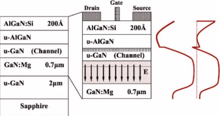
Mg-doped GaN is to isolate the leakage current of the buffer layer. The as-grown Mg-doped GaN layers were almost insulating. Three HFETs with different channel thicknesses of 1200, 1500, and 1800 Å were denoted HFET-12, HFET-15, and HFET-18, respec-tively. Figure 1 shows the cross section and energy band diagram of the Al0.32Ga0.68N/GaN HFETs. Device active regions were defined
using mesa etching by ICP-RIE 共inductively coupled plasma-reactive ion etching兲 using the Cl2/Ar plasmas. The etching rate was about 410 nm/min. Etching was followed by the formation of source-drain ohmic contacts by the rapid thermal annealing of ther-mally evaporated Ti/Al 共15 nm/100 nm兲 at 850°C for 30 s. Gate electrodes with a length of 1.2m were then defined by photoli-thography, Ni/Au共50 nm/70 nm兲 thermal evaporation, and liftoff, subsequently. On-wafer dc measurements were made using a Keithley 4200 semiconductor parameter analyzer.
aPresent address: Land Mark Optoelectronics Corporation, Yung-Kang, Tainan, Taiwan, 710.
bPresent address: Department of Materials Science and Engineering, National Dong Hwa University, 1, Sec. 2, Da-Hsueh Road, Shou-Feng, Hualien, Taiwan. z
E-mail: [email protected]
Figure 1.共Color online兲 Schematic cross section and energy band diagram
of HFET-12, HFET-15, and HFET-18.
Journal of The Electrochemical Society, 154共3兲 H131-H133 共2007兲
0013-4651/2007/154共3兲/H131/3/$20.00 © The Electrochemical Society H131
Results and Discussion
Table I compares Hall measurement of distinct structures at 300 and 100 K. At 300 K, the mobility and sheet carrier concentration of HFET-18 are 409 cm2/Vs and 1.18⫻ 1013cm−2, respectively.
These values are the highest among the three proposed HFETs. The mobility and sheet carrier density of HFET-12 are 147 cm2/Vs and
3.99⫻ 1012cm−2at 300 K, respectively. These values for HFET-12 are much lower than those of HFET-18 because of the depletion region between the Mg-doped GaN layer and the undoped GaN channel layer, where an electrical field exists from the bottom of the undoped GaN共channel layer兲 to the top of the Mg-doped GaN layer. The carriers in the undoped GaN layer are partly depleted by the Mg-doped GaN and others will be confined in the AlGaN/GaN het-erointerface to form 2-DEG. The electrical field across the depletion region is important in determining the mobility of the carriers con-fined in the channel. Thus, as the thickness of the undoped GaN channel layer increases, a greater carrier concentration is confined and the 2-DEG will suffer less from the electronic field because the confined carriers are farther away from the depletion region. There-fore, the HFET-18 has the largest carrier mobility and carrier con-centrations. As the temperature increases, the 2-DEG mobility falls, because the lattice scattering becomes stronger. A sheet carrier den-sity as high as 1–2⫻ 1013cm−2is obtained from the AlGaN/GaN
heterointerface because of the piezoelectric effect.
The lattice mismatch between GaN and the sapphire is respon-sible for the large dislocation density and then forms traps, enabling the carriers to be captured. Under nonthermal equilibrium condi-tions, these caught carriers become free carriers. Figure 2 plots the current-voltage characteristics of the unintentional doped GaN layer. After the Mg-doped GaN layer is removed, the unintentional doped GaN layer shows a relatively large buffer leakage current. When the voltage exceeds 8 V, the leakage current exceeds 100 mA. To re-duce the leakage current, a Mg-doped GaN layer is introre-duced to provide the channel with good confinement.
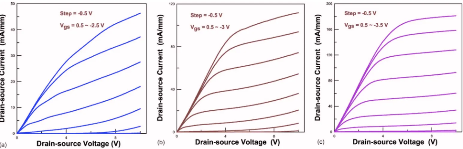
Figure 3a plots the IDS-VDS characteristics of FET-12 with VGS
from 1 to −2.5 V at 300 K. The excellent pinch-off characteristics are attributed to the use of the Mg-doped GaN layer. The value of
Idssis defined at Vgs= 0 V. Therefore, from Fig. 3a, the Idssvalue at
VDS= 10 V is 37 mA/mm for HFET-12. Figure 3b and c plots the
IDS-VDScharacteristics of HFET-15 and HFET-18, respectively. The
values of Idssfor HFET-15 and HFET-18 are 92 and 160 mA/mm,
respectively. The drain current density is directly proportional to the product of the electron mobility and the carrier density. Conse-quently, the results are consistent with the Hall measurement. The individual threshold voltages of HFET-15 and HFET-18 are −3 and
Table II. Comparisons of dc characteristic of the three HFETs and the PolFET (Ref. 13).
Devices HFET-12 HFET-15 HFET-18 PolFET
Lg共m兲 1.2 1.2 1.2 0.7 共cm2/Vs兲 147 395 409 826 IDSS共mA/mm兲 37 92 160 850 Gm共mS/mm兲 20 44 74 93 VB共V兲 25 21 18 — Vth共V兲 −2.5 −3 −3.5 −10 ft共GHz兲 — — — 18.6 fmax共GHz兲 — — — 44
Figure 2.共Color online兲 Leakage current of 2 m thick unintentional doped
GaN layer of the Al0.32Ga0.68N/GaN HFET.
Figure 3.共Color online兲 Current-voltage characteristics of 共a兲 HFET-12, 共b兲 HFET-15, 共c兲 HFET-18 with a gate areas of 1.2 ⫻ 100 m2at 300 K.
Table I. Hall measurements of the three Al0.32Ga0.68N/GaN HFETs. Temperature 共K兲 共cm2H/Vs兲 nS Hall ⫻1012共cm−2兲 Rsh 共⍀/ 䊐 兲 HFET-12 300 147 3.99 10,700 100 253 3.73 5520 HFET-15 300 395 9.01 1760 100 676 8.98 1030 HFET-18 300 409 11.8 1460 100 679 11.7 785
H132 Journal of The Electrochemical Society, 154共3兲 H131-H133 共2007兲
H132
−3.5 V, respectively. Because in HFET-18 a thick channel would have more carriers, its depletion therefore requires a higher negative voltage. The self-heating effect of the poor thermal conductivity of the sapphire substrate is not obvious, probably because the drain current density is not high enough.
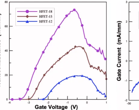
Figure 4 plots the maximum extrinsic transconductance共Gm,max兲 of the three proposed HFETs at 300 K. The Gm,maxvalues of HFET-18, HFET-15, and HFET-12 are 74, 44, and 20 mS/mm, respec-tively. As we can see in Fig. 4, Gm,maxwith respect to gate voltage is shifted towards the positive gate voltage for lower channel thickness because of the larger carrier density. Therefore, there is a relatively larger threshold voltage for HFET-18. The threshold voltage of an HEMT can be obtained by solving the one-dimensional Poisson’s equation as12
Vth=共⌿B/q兲 − 共⌬EC/q兲 − 共qNddd/兲
where⌿B is the Schottky barrier height of metal on the Schottky layer, ⌬EC is the conductance-band discontinuity between the Schottky layer and channel layer, Ndis the sheet concentration, ddis the distance between the gate and doping plane, and is the permit-tivity of Schottky layer. Among these three samples, all the structure conditions are the same except for the thickness of the undoped GaN channel layer. Hall measurement shows that the carrier concentra-tion 共Nd兲 decreases with the thickness of undoped GaN channel. Thus, from the above equation, Vth moves toward more positive values because of the decrease in the Nd. Figure 5 plots the two terminal gate-to-drain breakdown voltage共VGD兲 of the three HFETs.
VGD is defined as the voltage at which the leakage current is 1 mA/mm at 300 K. The values of VGDfor HFET-18, HFET-15, and
HFET-12 are −25, −21, and −18 V, respectively. Because HFET-18 has more carriers in the channel, it has a larger leakage current and lower breakdown voltage than the other two proposed HFETs. Table II compares the performance of the studied devices and the PolFET reported in Ref. 13. As we can see from the polarization-doped FET 共PolFET兲, the larger mobility results in larger Idss. For HFET-18, the
high frequencies characteristic was suppressed because of the lower mobility.
Conclusions
AlGaN/GaN HFETs were fabricated. Three structures with dif-ferent channel thickness are discussed. HFET-18 has a maximum saturation current density 共Idss兲 of 160 mA/mm and the highest transconductance共Gm,max兲 of 74 mS/mm because of its highest car-rier concentration. Moreover, a Mg-doped insulating GaN layer is inserted to suppress the leakage current, improving the breakdown voltages. Additionally, excellent pinch-off characteristics are achieved. The pinch-off voltages of HFET-18, HFET-15, and HFET-12 are −3.5, −3, and −2.5 V, respectively, because the more carriers in HFET-18 require a higher negative to be depleted.
National Cheng-Kung University assisted in meeting the publication costs of this article.
References
1. C. F. Shih, N. C. Chen, P. H. Chang, and K. S. Liu, J. Electrochem. Soc., 152, G816共2005兲.
2. J. K. Kim and J.-L. Lee, J. Electrochem. Soc., 151, G190共2004兲.
3. M.-W. Ha, S.-C. Lee, J.-C. Her, K.-S. Seo, and M.-K. Han, Electrochem. Solid-State Lett., 8, G352共2005兲.
4. S. Yoshida and J. Suzuki, Jpn. J. Appl. Phys., Part 2, 38, L851共1999兲. 5. M. A. Khan, Q. Chen, J. W. Yang, M. S. Shur, B. T. Dermott, and J. A. Hinggins,
IEEE Electron Device Lett., 17, 325共1996兲.
6. Y. F. Wu, B. P. Keller, P. Fini, S. Keller, T. J. Jenkins, L. T. Kehias, S. P. DenBaars, and U. K. Mishra, IEEE Electron Device Lett., 19, 50共1998兲.
7. C. H. Chen, S. Keller, G. Parish, R. Vetury, P. Kozodoy, E. L. Hu, S. P. Denbaars, and U. K. Mishra, Appl. Phys. Lett., 73, 3147共1998兲.
8. R. Li, S. J. Cai, L. Wong, Y. Chen, K. L. Wang, R. P. Smith, S. C. Martin, K. S. Boutros, and J. M. Redwing, IEEE Electron Device Lett., 20, 323共1999兲. 9. W. Q. Chen and S. K. Hark, J. Appl. Phys., 77, 5747共1995兲.
10. A. Bykhovski, B. L. Gelmont, and M. S. Shur, J. Appl. Phys., 81, 6332共1997兲. 11. J. M. Redwing, M. A. Tischler, J. S. Flynn, S. Elhamri, M. Ahoujja, R. S. Newrock,
and W. C. Mitchel, Appl. Phys. Lett., 69, 963共1996兲.
12. A. Mahajan, M. Arafa, P. Fay, C. Caneau, and I. Adesida, IEEE Trans. Electron Devices, 45, 2422共1998兲.
13. S. Rajan, H. Xing, S. DenBaars, and U. K. Mishra, Appl. Phys. Lett., 84, 1591 共2004兲.
Figure 4. 共Color online兲 Comparisons of transconductance of the three
HFETs. Figure 5.down voltage of the three HFETs.共Color online兲 Comparisons of two terminal gate-to-drain break-H133
Journal of The Electrochemical Society, 154共3兲 H131-H133 共2007兲 H133