Pixel Circuit with External Current Source to Achieve Fast Compensation for Variations of LTPS TFTs for AMOLED Displays
Chih-Cheng Hsu, Chun-Ming Lu, Po-Chun Lai, Po-Syun Chen, and Chih-Lung Lin
*National Cheng Kung University, Department of Electrical Engineering Tainan City 701, Taiwan
Phone: +886-6-2757575 ext.62338 Fax: +886-6-234-5482 E-mail: [email protected]
This work proposes a new pixel circuit of low-temperature polycrystalline-silicon thin-film transistors (LTPS-TFTs) for active-matrix organic light-emitting diode (AMOLED) displays, which combines parallel addressing scheme, current-programmed, and voltage-programmed methods. The proposed pixel circuit is used to compensate for the threshold voltage variations of driving TFT, and the current-resistance voltage drop in power line (I-R drop). Moreover, the proposed pixel circuit can avoid flicker and extend compensation time. The simulation results demonstrate that the relative current error rates are less than 5% and 1% as the variations of threshold voltage and I-R drop are ±0.5 V and -0.5 V, respectively.
1. Introduction
Low-temperature polycrystalline-silicon thin-film transistors (LTPS-TFTs) have been widely used in pixel circuits of active-matrix organic light-emitting diode (AMOLED) displays because of their high mobility and stable electrical characteristics [1]-[3]. However, the fluctuations of excimer laser annealing (ELA) cause variations in the electrical characteristics of LTPS-TFTs, such as threshold voltage (VTH) and mobility variations, which leads to the nonuniformity of OLED currents [4].
Therefore, many methods have been used to compensate for VTH
variations of TFTs to generate uniform OLED currents, such as current-programmed and voltage-programmed methods [5],[6].
The current-programmed method compensates for VTH and mobility variations accurately. However, it needs a longer programming time because of a low data current at low gray level [7]. Thus, the voltage-programmed method is widely used because the programming time of voltage-programmed method is shorter than that of current-programmed method. Moreover, the current- resistance voltage drop (I-R drop) in power line is a critical issue in conventional 2T1C p-type pixel circuit, which causes the degradation of OLED currents and nonuniformity of brightness.
The voltage-programmed pixel circuit presented by Dawson et al.
compensates for the VTH variations and I-R drops [8]. However, this pixel circuit uses too many signal lines and complex control signals. Therefore, many voltage-programmed pixel circuits have been proposed which reduce signal lines and simplify control signals [9]-[13]. Although previous pixel circuits compensate for variations of threshold voltage successfully, they still suffer from flicker. Moreover, these pixel circuits need data lines to provide voltages in compensation stage, data input stage, and other stages
in scan time of one row (TSCAN), which limits the compensation time (TCOMP) to be less or equal to the TSCAN. Furthermore, TSCAN
becomes shorter as the resolution of displays becomes higher, so the TCOMP is not long enough for these pixel circuits to complete the compensation. Therefore, the parallel addressing scheme was proposed which uses data line to provide voltages only in data input stage and the overlapped compensation stage to extend TCOMP [14].
This work proposes a new pixel circuit based on LTPS-TFTs which combines parallel addressing scheme, current-programmed and voltage-programmed methods to achieve fast compensation for VTH variations of TFTs, and extend the TCOMP to ensure the compensation is complete. Moreover, the proposed pixel circuit keeps cross voltage of OLED lower than the VTH of OLED in compensation stage to avoid flicker. Furthermore, the OLED currents of proposed pixel circuit have high immunity to the influences of I-R drops. Simulation results show that the current error rates are lower than 5% at different gray levels as VTH
variations of driving TFT are ±0.5 V, which confirm that the proposed pixel circuit generates high uniform OLED currents.
2. Circuit Operation
Fig. 1 shows the schematic and the timing diagram of the proposed pixel circuit which is composed of four p-type switching TFTs (T1, T2, T3 and T4), one p-type driving TFT (T5), two capacitors (C1 and C2). The SCAN1 is used to control the reset of node C and detections of VDD and the VTH of driving TFT. SCAN2 is used to control the data input. T5 is used to generate emission currents for OLED. The IREF is a large current, which is used to reduce the detecting time when the pixel circuit detects the VTH of the driving
TFT, and suppress the cross voltage of OLED in the compensation stage to prevent flicker. The VREF supplies the reference voltage for the proposed pixel circuit. VDATA, VDD, and VSS are voltages of data line, power line, and common line, respectively. The width and length of the driving TFT are 4 μm and 15 μm, respectively. The width and length of all switching TFTs are both 3 μm. The capacitances of C1 and C2 are 0.3 pF and 0.2 pF, respectively. The voltages of SCAN1 and SCAN2 are both from -7 V to 7 V. VDD
and VSS are 4.5 V and -4.5 V, respectively. VDATA is from 0.5 V to 3.5 V. VREF and IREF are -3 V and 3 μA, respectively. The VTH of OLED (VTH_OLED) is 4 V. The operation of proposed pixel circuit can be divided into three stages –compensation stage, data input stage, and emission stage. The details of operation in each stage are described as follows.
In compensation stage, SCAN1 is low to turn on T2, T3 and T4. SCAN2 is high to turn off T1. The voltage of node C (VC) will be reset to VREF through T2. Moreover, the pixel circuit detects the VTH of driving TFT by IREF as shown in the equation (1).
.
|}
|
{
DD A TH_ T5 2REF
K V V V
I = − −
(1) where K is μ·COX·W/L, and VTH_T5 is the VTH of T5. According to the equation (1), the K, and IREF are constant, so the voltage of node A (VA) will be discharged to a voltage which corresponds to the variations of VTH_T5 and VDD. Furthermore, since IREF is a large current, VA will be fast discharged to a low voltage, which is lower than VSS+VTH_OLED. Thus, VA can be calculated as the equation (2)..
|
|
_ 5K V I
V
V
A=
DD−
TH T−
REF (2) Therefore, the VTH_T5 will be sensed and stored in C2. Additionally, the voltage of node B (VB) is equal to VA because T3 is turned on.Therefore, the currents of driving TFT will not flow through the OLED, and the flicker can be avoided. Furthermore, since T1 is off in this stage to prevent data voltages applied to the pixel circuit, the period of this stage can be extended by overlapping compensation stages of pixel circuits in different rows.
During data input stage, SCAN1 goes high to turn off T2, T3 and T4. SCAN2 goes low to turn on T1. VDATA is applied to node C through T1, and node A is floating. Thus, VA is coupled by C1 and C2 to the required driving voltage, which is used to generate OLED current and presented in the equation (3).
).
(
2 1 5 1
_ REF DATA REF
T TH DD
A
V V
C C
C K
V I V
V −
+ +
−
−
=
(3)
Finally, in emission stage, SCAN1 remains high and SCAN2 changes from low to high to turn off all switching TFTs. VB
becomes VSS+ VOLED, where VOLED is cross voltage of the OLED in this stage. Therefore, the pixel circuit applies emission current, which is generated by the driving TFT in saturation region, to OLED. The OLED current follows the equation (4):
. ) (
SG TH_ T5 2OLED
K V V
I = −
2 5 _ 2
1 1
5 _
} )
)(
( {
T TH REF DATA
T REF TH DD DD
V V
C V C
C
K V I
V V K
− + −
−
+ +
−
=
. )}
)(
(
{
22 1
1 DATA REF
REF
V V
C C
C K
K I −
− +
=
(4) From the equation (4), the OLED current is independent of the VTH of the driving TFT and the VDD. Therefore, the effect of VTH variations of driving TFTs, and I-R drop of power line can be eliminated by the proposed pixel circuit.
3. Simulation Results
This work used HSPICE software to simulate the VA, VC, and OLED current for confirming the compensation capabilities of the proposed pixel circuit. Fig. 2(a) shows that the transient waveforms of VA and VC in every stage when the VTH variations of driving TFT are 0.5 V and -0.5 V. The transient waveforms of VA
demonstrate that the pixel circuit senses the VTH_T5 very quickly.
Moreover, the pixel circuit sensed the voltage differences of VA, which is almost identical to the variations of VTH, when VTH
variations are 0.5 V and -0.5 V, and the voltage differences will be kept until next compensation stage. Furthermore, the VA in the compensation stage, is lower than -0.5 V, which is the voltage of Fig. 1. Schematic of pixel circuit and timing diagram of proposed circuit
VSS+VTH_OLED. The simulated results of VA ensure that the proposed pixel circuit can avoid flicker and achieve fast compensation for VTH variations of driving TFTs. The OLED currents of the proposed pixel circuit are simulated to confirm the influences of VTH variations on the OLED currents. Fig. 2(b) plots the OLED currents versus the different data voltages as the VTH
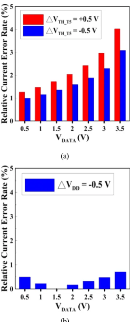
variations of driving TFT are 0.5 V and -0.5 V. The simulated results verify that the OLED currents present high uniformity at every gray level when the proposed pixel circuit suffers from the variations of VTH. Fig. 3(a) plots the relative current error rates versus different data voltages when the variations of VTH are 0.5 V and -0.5 V. The results demonstrate that the relative current error rates are all lower than 5%, which verify that the OLED currents have high immunity to VTH variations. Additionally, to confirm the influence of I-R drops on OLED currents, the simulations evaluate the relative current error rates at every gray level when power line has I-R drops. Fig. 3(b) plots the relative current error rates versus different data voltages as the I-R drop of the power line is -0.5 V.
The simulated results show that the relative current error rates are all lower than 1% and verify that the proposed pixel circuit has the capability to compensate for I-R drops to generate uniform OLED
currents. Therefore, the results of simulations verify that the proposed pixel circuit compensates for variations of VTH and I-R drops successfully, and the OLED currents of the proposed pixel circuit have high uniformity at every gray level and high immunity to VTH variations and I-R drops.
4. Conclusions
This work proposes a new LTPS-TFTs pixel circuit that combines parallel addressing scheme, current-programmed and voltage-programmed methods to compensate for variations of VTH
of TFTs, and I-R drops of power line. The simulation results demonstrate the relative current error rates are all below 5% when variations of VTH are ±0.5 V and all below 1% when I-R drop is -0.5 V, which verify that the proposed pixel circuit has high immunity to VTH variations of TFTs, and I-R drops. The proposed pixel circuit achieves fast compensation and generates high uniformity OLED currents. Therefore, the proposed pixel circuit is suitable for use in AMOLED display.
(a)
(b)
Fig. 2. (a) Transient waveforms of VA and VC of proposed pixel circuit. (b) OLED currents versus data voltages of proposed pixel circuit.
(a)
(b)
Fig. 3. (a) Relative current error rates with ±0.5 V variations of TFT VTH
for proposed pixel circuit. (b) Relative current error rates with 0.5V VDD
drop for proposed pixel circuit.
Acknowledgments
This work was supported in part by the Advanced Optoelectronic Technology Center, National Cheng Kung University, Tainan, Taiwan, and the Ministry of Science and Technology of Taiwan under Projects of MOST 105-2218-E-006-009 and MOST 105-2622-E-006-033-CC2, as well as AU Optronics Corporation is appreciated for its technical and funding support
References
1) C. L. Lin, and Y. C. Chen: IEEE Electron Device Letters, vol. 28, no. 2, Oct 2007, pp. 129-131.
2) C. L. Lin, W. Y. Chang, C. C. Hung, and C. D. Tu: IEEE Electron Device Letters, vol. 33, no. 5, May 2012, pp. 700-702.
3) J. P. Lee, H. S. Jeon, D. S. Moon, and B. S. Bae: IEEE Electron Device Letters, vol. 35, no. 1, Jan. 2014, pp. 72-74 .
4) S. H. Jung, W. J. Nam, and M. K. Han: IEEE Electron Device Letters, vol. 25, no. 10, Oct. 2004, pp.690-692.
5) S. J. Ashtiani, P. Servati, D. Striakhilev, and A. Nathan: IEEE Transactions on Electron Devices, vol. 52, no. 7, Jul. 2005, pp. 1514-1518.
6) W. J. Wu, L. Zhou, R. H. Yao, and J. B. Peng: IEEE Electron Device Letters, vol. 32, no. 7, Jul. 2011, pp.931-933.
7) J. H. Lee, W. J. Nam, S.H Jung, and M.K Han: IEEE Electron Device Letters, vol. 25, no. 5, MAY. 2004, pp. 208-282.
8) R. Dawson et al.: IDEM Tech. Dig., 1998, pp.875-878.
9) H. Y. Lu, P. T. Liu, T. C. Chang, and S. Chi: IEEE Electron Device Letters, vol. 27, no.9, Sep. 2006, pp.743-745.
10) C. L. Lin, T. T. Tsai, and Y. C. Chen: IEEE/OSA Journal of Display Technology, vol. 4, no.1, Mar. 2008, pp.54-60.
11) C. L. Lin, C. C. Hung, P. S. Chen, P. C. Lai, and M. H. Cheng: IEEE Transactions on Electron Devices, vol. 61, no. 7, Jul. 2014, pp. 2454-2458.
12) C. L. Lin, P. S. Chen, M. H. Cheng, Y. T. Liu, and F. H. Chen:
IEEE/OSA Journal of Display Technology, vol. 11, no. 2, Feb. 2015, pp.
146-148.
13) C. Wang, C. Leng, L. Wang, W. Lu, and S. Zhang: IEEE/OSA Journal of Display Technology, vol. 11, no. 7, July 2015, pp. 615-619.
14) C. L. Lin, P. C. Lai, P. C. Lai, and P. S. Chen: IEEE Journal of the Electron Devices Society, vol. 4, no. 6, Nov. 2016, pp.436-440.