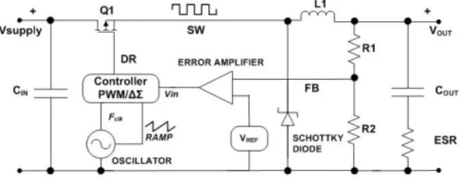
Figure 1. Block diagram of DC-DC converter based on buck
A Delta-Sigma based DC to DC Converter - A Design Space Exploration
Kamala Hariharan
Student Member, IEEE Santa Clara University 500,El Camino Real, Santa Clara, CA-
95052 [email protected]
Shoba Krishnan
Member, IEEE Santa Clara University 500, El Camino Real, Santa Clara, CA-
95052 [email protected]
Susan Luschas
Member, IEEE Santa Clara University 500, El Camino Real, Santa Clara, CA-
95052
[email protected]
Abstract -- Traditional pulse-width modulation (PWM) in a DC-DC converter offers high efficiency but has large spurs occurring at integer multiples of the clock frequency. An alternate architecture using the delta sigma (ΔΣ) controller is studied and compared for theoretical spurious performance and efficiency. Tradeoffs in selecting the delta-sigma order, over sampling ratio (OSR), and input voltage (Vin) range are investigated. While a large OSR and high order can reduce the magnitude of the spurs and push them out to a higher frequency, the power efficiency of the system is compromised.
This paper aids designers in exploring the design space for the optimal ΔΣ parameters given efficiency and spurious performance specifications..
Index Terms—DC-DC Converter, Delta Sigma Modulation, FFT, Efficiency, OSR, Order
I. I
NTRODUCTIONDC-DC converters are architectures that convert a DC input voltage to a stable and unvarying DC output voltage.
These converters are mainly classified into two categories.
They are Linear Drop Out Regulators (LDO) and switching regulators [1].LDOs regulate the output by behaving as variable resistors between the input and output. While these architectures offer extremely low ripple at the output, they have low efficiency since they continuously dissipate power across the variable resistor. Switching regulators use a clocked signal to generate current in an inductor that is proportional to the load requirements. Since an ideal inductor and ideal switch are lossless components, switching regulators have high power efficiency at the expense of a more complex architecture and noise performance.
Switching regulators typically use pulse width modulation (PWM) as the control scheme for regulation. These controllers switch every clock cycle to maintain the regulated output voltage. This switching noise manifests itself in the form of ripple at the output in the time domain and as spurs at discrete multiples of the clock frequency (F
clk) in the frequency domain. The noise directly couples into the components that draw current from the regulator.
The block diagram in Figure 1 shows a buck converter using a PWM controller. The control loop consisting of the feedback resistors R1 & R2, error amplifier with the compensation network (not shown in figure) and the PWM Controller is the basic loop used in conventional DC to DC
converters. The DR node is the controller output that makes transistor Q1 switch periodically such that the waveform at the SW node resembles a square wave. Since the DR node is controlled by F
clk, the frequency at the SW node is identical to F
clk. Fourier analysis theory states that the DC component of a periodic waveform is equal to its average value [1].
Hence by adjusting the duty cycle of the square waveform, variable output voltages can be obtained. L1, C
outand the parasitic resistance ESR together act as a low pass filter to provide the averaged output. The compensation network is designed to stabilize the system. By selecting the filter cutoff frequency to be much smaller than the switching frequency, an output voltage that has very small ripple can be obtained.
An alternative control solution to reduce the clock spurs of the PWM using the noise shaping characteristics of the delta sigma (ΔΣ) modulator is described in [2-6]. It has been shown that the ΔΣ can replace the PWM controller in Figure 1 and still retain the properties of the conventional switching regulator. The error amplifier with its external compensation network is similar to that required by the conventional PWM based controller since the poles and zeros of the ΔΣ controllers are located well above the loop crossover frequency created by the compensation network [2]. The ΔΣ controller uses the pulse density modulation (PDM) technique to maintain its output voltage by producing a variable train of pulses. As a result, its switching frequency will be different from the clock frequency F
clk.
ΔΣ modulators consist of integrators connected in a feedback loop so that the average output equals the average of the input signal. The feedback via the integrator shapes the modulation noise, placing most of its energy outside the signal band [7].
The noise shaping property of the ΔΣ modulator causes randomization in the switching of the SW node of Figure 1, such that transistor Q1 may not switch every clock cycle.
PEDS2009
This study targets applications such as cell phones and wireless communication systems where both high efficiency and excellent spurious noise performance are desired. It is shown that the design of these systems using the ΔΣ controller involves an optimal choice of design parameters.
Section II analyzes the PWM and ΔΣ topologies for spurious performance and power efficiency. The system behavior for different output voltage specifications and for variations in the design parameters such as over sampling ratio (OSR) and order are examined in Section III. The paper concludes by exploring the design space that helps select the appropriate ΔΣ parameters for optimal buck converter performance.
II. C
ONTROLLER PERFORMANCEM
ETRICSSpurious performance and power efficiency are the most critical specifications for switching regulators and are described in this section.
A. Spur performance
Spurs are an important metric for switching regulators as their magnitude and frequency of occurrence determine the size of the output filter. If not filtered appropriately, the spurs may couple into the circuits that they drive. This could cause, for example, a wireless transceiver to not meet FCC regulations. In addition to the traditional evaluation of the ripple in the time domain, it is critical to examine the performance in the frequency domain.
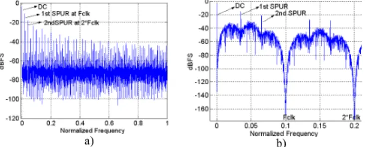
The spurs can be measured by performing a Fast-Fourier transform (FFT) on the node DR in Figure 1. Figure 2a and Figure 2b show the FFTs of the PWM and ΔΣ systems respectively depicting the location of the first and second high energy tones with respect to F
clk. The spurs at multiples of F
clkfor the PWM controller are clearly visible in Figure 2a.
For the ΔΣ system, the spurs are located below F
clkvalue but
much higher than the loop crossover frequency (not shown in figure) created by the compensation network in the error amplifier. This frequency is set so that it lies in the in-band of the ΔΣ modulator. The lower the frequency of the spur, larger components and/or a more complicated filter with a steep roll-off may be required.
B. Efficiency
Efficiency is a measure of the power dissipated in a system.
For a DC-DC converter the efficiency is given by η= P
out/P
Supplyin % (1)
where P
out=Output power and P
supplyis the input power given by (2).
P
supply= P
out+ P
loss(2) where P
loss= P
static+P
trans+P
Cg+ P
MOS(3)
where P
staticoccurs due to the load current and the parasitic resistance present in the inductor; P
transrelates to the power loss that occurs due to the finite rise and fall times; P
Cgis the power lost in charging and discharging of the gate capacitance (C
g) of Q1 during switching and P
MOSindicates the conduction losses that arise due to the finite resistance of the switch Q1 [8]. Since the PWM and the ΔΣ based buck converters differ only in the MOSFET gate drive waveform (node DR in Figure 1), the static loss contribution is the same and hence is not considered for comparison. The other three loss terms depend on how often the gate of Q1 is switched and therefore contribute to the efficiency difference between the two systems.
To compare the performance of the two systems, a typical cell phone application using a buck converter was chosen with its input supply voltage V
supplyat 3.5V and driving a load current of 2A. In-band was defined as 0-200 KHz, which is typically the bandwidth of such systems in these applications [7, 8]. The resistance of Q1 was assumed to be 25mΩ, and its gate capacitance C
gto be 5nF. The rise and fall times of the DR signal were assumed to be 2.5ns.
III. ΔΣ S
YSTEM PARAMETERE
XPLORATIONThe performance of the ΔΣ controller is dependent on its input voltage (V
in) relative to full scale, the oversampling ratio (OSR) and the order. Reference [9] provides a mathematical relation between the in-band noise power and each of the above parameters. The ΔΣ toolbox in Matlab
™was used to create the controller models. The controller input, V
in, is essentially the same for both cases [9, 10]. The high frequency spurs were simulated by performing the FFT on these models as shown in Figure 2. The efficiency was calculated by measuring the number of transitions over a time period. The two systems were assumed to have the same filter requirements and loop dynamics in order to make a direct comparison. Addition of dither to the systems can help reduce spur magnitudes in both the delta-sigma and PWM systems [3,4]. However, no dither was added at the DR node for either of the two systems for simplification of their analyses.
A. Output Voltage Variation
Changes in the output loading or changes in the supply cause a proportional change in V
into the controller in Figure 1. This design parameter is fixed for a given value of V
supplyand
a) b)
Figure 2. FFT of DR signal for a) PWM and b) ΔΣ based DC-DC converters showing 1st and 2nd spurs. Fclk =12.8 MHz, loop cross over frequency=200KHz
PEDS2009
V
OUT. In the PWM case, this variation causes a corresponding change in the duty cycle of the DR signal of Figure 1. A ΔΣ modulator with order 2 and OSR of 64 was chosen as the baseline for understanding the system performance for V
invariation. The choice for the order and OSR was dominated by the noise shaping and simplicity of the architecture [11]. V
inwas varied between +/-0.8, referenced to a full scale of 1. This corresponds to a duty cycle variation between 10 and 90% in the PWM system with V
inof 0 corresponding to a duty cycle of 50%. Figure 3a and Figure 3b show the variation of spur magnitudes and spur frequency respectively with V
infor the two systems. The spurs were measured relative to the DC value of the output as shown in Figure 2 (dBc).
For the PWM based system, the switching frequency does not change with the variation in duty cycle. Hence the spurs remain at integer multiples of the clock frequency. As the duty cycle varies, the magnitude of the spurs changes. This is because the location of the zeros (nulls) in the sinc function shift as the duty cycle changes. As V
inapproaches mid-scale, the spur occurring at even multiples of F
clkland in nulls of the sinc function, leaving only odd harmonics of F
clk[12].
For the ΔΣ system, as V
inincreases the number of transition pulses for a given time period increase thus causing the spur magnitude to decrease. As V
inapproaches mid-scale, the ΔΣ output transitions every two clock cycles. This resembles the PWM system running at F
clk/2 and the maximum spur occurs here. As V
inincreases further, the duty cycle approaches its maximum value, thus decreasing the number of transitions in the ΔΣ, and a subsequent reduction in spur magnitude and frequency. The same phenomenon occurs as V
inreaches its minimum value. From Figure 3a & 3b it is seen that while the spur magnitudes of the 1
stand 2
ndspurs for the ΔΣ are lower than the PWM, they are located at frequencies lower than F
clk. The ΔΣ also shows significantly lower spur magnitude at F
clkwhen compared to the PWM system.
Figure 3c shows the efficiency with varying V
infor the two systems. From the graph it is seen that the efficiency of the ΔΣ is higher than the PWM operating at the same clock frequency. This is due to the fact that the ΔΣ controller does not switch every clock cycle to maintain the output in regulation. With fewer transitions, the ΔΣ has reduced P
Cg, resulting in an increase in efficiency.
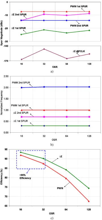
B. ΔΣ Design Parameters Variation 1) Choice of Over Sampling Ratio (OSR) :
This section quantifies the effect of various oversampling ratios on the ΔΣ spurious performance. Increasing the over- sampling ratio corresponds to an increased clock frequency relative to the fixed signal bandwidth of 200KHz. To analyze the performance of the ΔΣ controller, a 2
ndorder system with V
inat 0.3V was chosen as a benchmark. The V
inwas chosen to be close to the mid-scale value but below the two extremities corresponding to maximum and minimum duty cycles. Figure 4a and Figure 4b show the variation of spur magnitude and spur frequency with OSR relative to F
clkfor the two systems.
For the PWM based system, an increase in OSR results in an increase in F
clk. The spur magnitude remains constant due to
the fixed duty cycle D and does not change with increased F
clk. The spur frequency increases linearly due to the increase in F
clk. For the ΔΣ modulator, also increasing OSR causes an increase in F
clk.The in band noise floor is reduced by pushing the noise to higher frequencies. The spur magnitudes for the 1
stand 2
ndspurs remain relatively constant for increasing OSR. The spur frequency increases as expected because of the increase in the F
clk. Due to the normalized frequency scale used in Figure 4b, the location of spur remains constant. The
a)
b)
c)
Figure 3 . Response of the PWM and ΔΣ for variation with Vin a) Spur Magnitude (dBc) b) Spur Frequency normalized to Fclk and c)Efficiency. A
2nd order ΔΣ system with OSR=64 was used for these simulations.
PEDS2009
spur magnitude of the ΔΣ at the F
clkis again lower than the PWM system.
Figure 4c shows the variation in efficiency with OSR. As the OSR increases, the efficiency decreases because the P
Cgand P
translosses become significant with increasing frequency.
The ΔΣ controller has fewer output transitions to regulate the output voltage and therefore shows better efficiency.
Increasing OSR pushes the spurs to higher frequencies and reduces the in-band noise floor thereby easing the filtering requirements. On the other hand, the efficiency of the system is compromised due to the increased clock frequency.
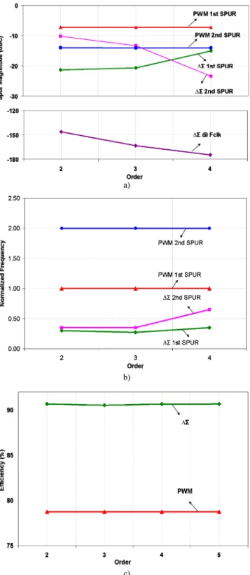
2) Selection of Order:
The variation in order in a ΔΣ modulator relates to increasing the number of integrators in its feedback loop. To study the performance of the ΔΣ modulator with order, Vin was fixed at 0.3V and an OSR of 32 was chosen. The PWM system shows no variation with ΔΣ order and is only used as a reference. Figure 5a shows the spur magnitude of the ΔΣ system for variation in order. As the order increases, the output becomes more randomized which causes the magnitude of the 1st spur to increase and the 2nd spur to decrease. Figure 5b shows the spur frequency for variation in order. The 1st spur frequency remains relatively constant for increasing order and occurs below F
clk/2. The frequency of the 2
ndspur on the other hand, increases with order. The spur magnitude at the clock frequency is again found to be lower than the PWM system. Although the magnitudes of the 1
stspur increase with order, they are located at a much higher frequency than the bandwidth of interest and therefore can be easily filtered .Figure 5c shows the variation of the efficiency with order of the ΔΣ system. The efficiency remains relatively constant as the overall number of transitions in the ΔΣ system remains constant.
Increasing the order in a ΔΣ system can aid in better noise shaping and reduction of spur magnitude but at the cost of higher complexity of the architecture and increased out-of- band noise.
C. Design Selection
A design guideline for controller selection can be established by using the above simulation results. For example, A typical cell phone application requiring about 90% efficiency, can be achieved by the ΔΣ system for V
ingreater than 0.5V with a 2
ndorder and OSR=64, as evident in Figure 3c. This corresponds to a buck converter having a duty cycle greater than 75%. Another choice for the same application would be for a 2nd order system with V
inset at 0.3V and OSR lesser than 32 as inferred from Figure 4c which corresponds to 65% duty cycle in the buck converter.
IV. C
ONCLUSIONThe conventional PWM and the ΔΣ based DC-DC converters are compared for their efficiency and spurious performance. The ΔΣ based controller reduces magnitude of the spurs at the clock frequency but has spurs that occur at frequencies lower than F
clk. The spur magnitude and frequency of the ΔΣ resemble the PWM system switching at F
clk/2 as V
inapproaches mid scale. An optimum choice for the order and OSR exist for the ΔΣ based controller given the
a)b)
c)
Figure 4. Response of the PWM and ΔΣ for variation with OSR a) Spur Magnitude (dBc) b) Spur Frequency relative to Fclk and c)Efficiency. A 2nd
order ΔΣ system with Vin=0.3V was used for these simulations.
PEDS2009
spur performance, efficiency and V
inspecifications. As OSR increases, the spurs are pushed out in frequency, improving noise performance and alleviating the filtering requirements.
However, this sacrifices efficiency. As ΔΣ order increases, the
magnitude of the 2
ndspurs are again reduced as they are pushed out in frequency, due to increased randomization of the ΔΣ output. This paper shows that for certain spur frequency, spur magnitude, and efficiency specifications, the ΔΣ controller can out-perform the PWM.
V. R
EFERENCES[1] Ericson,Maksamovic,”Fundamentals of power electronics”, Kluwer publishers, 2002
[2] Steven K. Dunlap, Terry S. Fiez, “A Noise Shaped Power Supply Using a Delta Sigma Modulator,” IEEE Transactions on Circuits and Systems,vol.51, No.6 ,pp. 1051-1061, June 2004
[3] C. H. Bae, J. H. Ryu and K. W. Lee, " Suppression of Harmonic Spikes in Switching Converter Output Using Dithered Sigma-Delta Modulation," IEEE Trans. on Indus. Appli., vol. 38, no. 1, pp 159 – 166, January 2002.
[4] S. J. Finney, T. C. Green and B. W. Williams, " Spectral Characteristics of Resonant-Link Inverters," IEEE Trans. on Power Elec., vol. 8, no. 4, pp 562 – 570, October 1993.
[5] J. Paramesh and A. V. Jouanne, " Use of Sigma-Delta Modulation to Control EMI from Switch-Mode Power Supplies," IEEE Trans. on Indus. Elec., vol. 48, no. 1, pp 111 – 117, February 2001.
[6] A. Hirota, S. Nagai and M. Nakaoka, " A Novel Delta-Sigma Modulated DC-DC Power Converter utilizing Dither Signal," pp. 831 – 836 1999
[7] “MIC4724 3A, 2MHz Integrated switch Buck Regulator with 6V max input”, Datasheet-Micrel Semiconductor
[8] “LTC3545-Triple 800mA Synchronous Step down Regulator- 2.25MHz”, Datasheet -Linear Technology Corp.
[9] Richard Schreier, Gabor .C. Temes,”Understanding Delta Sigma Data Converters”, IEEE Press, 2005
[10] Delta Sigma Toolbox Users Guide, Version 7.1,The Matworks Inc, Natick, MA, 2008
[11] James C. Candy, Gabor. C. Temes,”Oversampling Methods for A/D and D/A Conversion”, an article in “Oversampling Delta Simga Data Converters Theory, Design and Simulation”, IEEE press, 1991 [12] Sanjit K. Mitra , “Digital Signal Processing, A Computer based
approach”, Third Edition,Mc-Graw Hill ,2006.
[13] Travis Eichhorn,”Comparing the calculated vs measured efficiency loss in synchronous buck converters”,EE times , Oct 2006
a)
b)
c)
Figure 5 . Response of the PWM and ΔΣ for variation with order a) Spur Magnitude (dBc) b) Spur Frequency relative to Fclk and c)Efficiency. A ΔΣ
system with Vin=0.3V & OSR= 32 was used as the test setup.