行政院國家科學委員會專題研究計畫 成果報告
軟體無線電系統晶片--子計畫二:軟體無線電基頻電路與 頻率合成器
研究成果報告(精簡版)
計 畫 類 別 : 整合型
計 畫 編 號 : NSC 97-2221-E-011-142-
執 行 期 間 : 97 年 08 月 01 日至 98 年 10 月 31 日 執 行 單 位 : 國立臺灣科技大學電機工程系
計 畫 主 持 人 : 陳筱青
計畫參與人員: 碩士班研究生-兼任助理人員:郭家豪 碩士班研究生-兼任助理人員:張書維 碩士班研究生-兼任助理人員:涂柏榕 碩士班研究生-兼任助理人員:黃麟翔 碩士班研究生-兼任助理人員:金彥呈
報 告 附 件 : 出席國際會議研究心得報告及發表論文
處 理 方 式 : 本計畫涉及專利或其他智慧財產權,2 年後可公開查詢
中 華 民 國 99 年 01 月 14 日
行政院國家科學委員會補助專題研究計畫 ■ 成 果 報 告
□期中進度報告 軟體無線電基頻電路與頻率合成器
計畫類別:■ 個別型計畫 □ 整合型計畫
計畫編號:NSC 97 - 2221 - E - 011 - 142 - 執行期間: 97 年 8 月 1 日至 98 年 10 月 31 日
計畫主持人:陳筱青 共同主持人:
計畫參與人員: 張書維,郭家豪,黃麟翔,涂柏榕,金彥呈
成果報告類型(依經費核定清單規定繳交):■精簡報告 □完整報告
本成果報告包括以下應繳交之附件:
□赴國外出差或研習心得報告一份
□赴大陸地區出差或研習心得報告一份
■出席國際學術會議心得報告
□國際合作研究計畫國外研究報告書一份
執行單位:台灣科技大學電機系(所)
中 華 民 國 99 年 1 月 12 日
摘要
本計畫是整合型計畫「軟體無線電系統晶 片」中的子計畫二「軟體無線電基頻電路與 頻率合成器」,主要負責接收機的基頻電路,
還有控制頻道選擇的頻率合成器電路的研 製。
我們所採用的基頻電路架構是取樣式電 路,因為在信號送入類比數位轉換器之前是 已經被取樣過的信號,自然就可以降低對於 類比數位轉換器規格上的要求。其次,濾波 器的頻寬會是取樣頻的函數,因此只要調整 取樣頻率就可以任意地調整濾波器的頻寬。
對於會在許多不同的頻道範圍之間切換的 SDR 系統,這樣的架構大大地提昇接收機的 靈活度。此外要利用時脈產生電路來產生這 些控制信號/取樣時脈。這個時脈產生器除了 必須產生多種頻率的時脈,還要產生多種相 位的時脈。
在本計畫裡我們決定研製分數型頻率合成 器,並用它來產生收發系統中的本地振盪信 號。在壓控振盪器的研製上,利用差動電壓 控制可變電容時,可以將VCO 電路裡在可變 電容部份的共模雜音抵消,如此一來可變電 容的雜音可以被大大的降低。本子計畫希望 能將此種相位雜音低而可調頻率又寬的 VCO 應用於鎖相迴路之中,做為軟體無線收發機 中頻率合成器的最佳方案。另一方面的研究 是 關 於 利 用 transformer-C 做 為 共 振 腔 的 VCO。調整流過 transformer 的兩個線圈的電 流之間的比例,就可以達成改變VCO 的振盪 頻率。將可變電容的控制電壓與電流源的偏 壓結合在一起,形成單一電壓輸入型式,可 以使得整個鎖相迴路變得比較簡單。將這種 架構與差動電壓控制可變電容 VCO 架構結 合,使其互相截長補短,這個新型的VCO 就 能達成更寬的可調頻率與更低的相位雜音。
關鍵詞
軟體無線電,縮減取樣濾波器,頻率合成器 一、 前言
軟體無線電的定義其實尚未被明確地界 定,對很多人來說它和 reconfigurable radio 其實很相近,只要無線電系統的載波可以調 整到各個頻帶去進行收發動作,而它的基頻 電路可以處理各種信號調變,也支援各種通 道寬度,就可以算是軟體無線電。也就是說,
軟體無線電系統是一個功能十分多樣化的系 統,只要靠記憶體儲存的資訊以及微處理機 發命令,使用者就能藉由這樣一個無線電系 統來使用各種無線通訊服務。軟體無線電的 概念最早是由 Mitola 在 1995 年所提出的想 法,它的精神在於系統中唯ㄧ的類比電路是 可操作在射頻頻帶的資料轉換器[1]。所有的 無線系統所提供的功能都是由一個可程式的 數位信號處理器來提供。但是這種作法中的 資料轉換器所消耗的功率其實相當驚人,雖 然整個系統俱備了很優良特性,但實在不符 合一般民眾的需求。因此我們所秉持的研究 方向是要完成一個低成本,但足以提供一般 民眾所常會用到的無線電服務的軟體無線電 系統。
二、研究目的
目前關於軟體定義無線電的研究在國內電 子學門尚未受到重視,然而在國外實際上卻 已經有許多研究團隊在關心這個議題。以比 利時Leuven 大學的 Dr. Craninckx 為主的研 究團隊,在今年ISSCC 會議上發表了一個在 130nm CMOS 製程下實現的軟體定義無線電 收發機[2]。Dr. Craninckx 的架構是以可調整 式射頻電路搭配可調整式基頻電路所達成的 軟體定義無線電收發機。然而在這篇論文 中,確有一些實際上的問題。首先是在射頻 前端電路之前所置放的一個微機電式開關,
以針對不同頻帶切換相對應的匹配電路。從 應用的角度看起來,前端的開關與匹配電路 會因為要支援的系統種類變多而變得很複 雜,且耗費更多生產成本。此外在類比基頻 電路的方面,他們是利用切換電容電阻與 OTA 的數目來達成基頻電路的可變增益與 低通濾波的轉角頻率,整個電路特性會因此 嚴重地受到製程偏移的影響。
美國UCLA 的 Abidi 教授所指導的研究團 隊,在今年ISSCC 會議上發表了一個在 90nm CMOS 製程下實現的軟體定義無線電接收機 [3-4]。與 Craninckx 不同的是他是利用數位
3
信號處理的觀念去設計濾波器,因此還可以 一併處理反混疊失真的問題。然而,所有相 關於軟體定義無線電的研究在頻率合成器這 邊,都是採用兩個以上的鎖相迴路來達成寬 頻內的載波合成,對於要以精簡的型式來完 成一個軟體無線電收發系統,的確還有很大 的努力空間。
三、研究方法
本計畫為三年期之計畫,全程執行期限為 民國97 年 8 月 1 日至民國 99 年 7 月 31 日。
本年度為計畫執行之第一年度,原本預計完 成之工作項目有:基頻電路的子電路(主要包 含高階的縮減取樣濾波器以及多頻率多相位 的時脈產生器)的電路設計、電路模擬、電路 佈局以及下線製作。頻率合成器的主要子電 路為電壓控制振盪器(VCO)的電路設計、電 路模擬、電路佈局以及下線製作。此外我們 必須要將頻率合成器的系統分析完成。
類比基頻電路
類比基頻電路的部份主要為縮減取樣濾 波 器 如 圖 一 所 示 , 在 申 請 計 畫 時 已 完 成 Gm-cell 與切換開關電容陣列的設計與模 擬,本年度主要進度為完成控制開關的時脈 產生電路設計。時脈產生電路的部份我們是 利用 verilog code 去把所需要的時脈控制產 生出來,再去合成實體電路。
圖一縮減取樣濾波器架構圖
此外我們另外利用Gm-C 架構完成了一個 傳統式的類比濾波器。為了超越先前技術,
我們設計了一個可程式頻寬的低通-帶通雙 模濾波器。本電路為多頻段可調式濾波器架
構,應用頻段有 5MHz、10MHz、20MHz、
25MHz 以及 30MHz,分別為 W-CDMA、IEEE 802.11a 、 IEEE802.11b 、 IEEE802.11g 及 IEEE802.16a 之應用頻段,預計將擴增至 200KHz 及 1MHz 之頻段。二階複數型帶通 濾波器架構圖如圖二所示,我們利用可程式 電容陣列來製作C1 和 C2,由於此兩個電容 同時掌管帶通濾波器的中心頻率與頻寬,因 此我們可以讓中心頻率與頻寬的比例成一固 定值(1~2,在本計畫我們選定此比例為 2),達 成一般low-IF 接收機架構中所需要的帶通濾 波器規格。由於濾波器對於通道外以及鏡頻 帶必須要有50~60 dB 的抑制,因此我們利用 三個二階複數型帶通濾波器來達成這個規 格,如圖三所示。
圖二 二階複數型帶通濾波器架構圖
圖三 六階複數型帶通濾波器架構圖
六階複數型帶通濾波器同時也具備低 通濾波器的功能,只要將圖二中的GM3,4 關掉,就能從複數型帶通濾波器變成低通 濾波器。因此不論最後接收機是採用直接 降頻架構或是低中頻架構,這個雙模式的 可程式濾波器都可以提供良好的通道選 擇。由於審查委員於去年有提出一個問 題,就是到底先前的縮減取樣濾波器和這 種傳統的Gm-C 濾波器有何不同。根據我 們的研究,發現縮減取樣濾波器所提供的 null 可以對於強大的 blocker 有非常好的 抑制效果。因此結論就是,如果採用傳統 Gm-C 濾波器,接收機仍必須使用頻帶選 擇濾波器去解決 blocker 的問題,但這需 要頻率可調的High-Q MEMS 濾波器,基 本上已經超出本計畫的範圍,因此在此我 們不多加討論。
頻率合成器
頻率合成器的架構圖如圖四(a)所示,它 包含有壓控震盪器(VCO,如圖四(b)所示),
可程式化除頻器,相頻偵測器(PFD),電荷 泵浦(CP),迴路濾波器(LPF),MASH3 三 角積分調變器。
(a)
(b)
圖四 (a)頻率合成器架構圖(b)壓控震盪器電 路圖
我 們 所 提 出 的 系 統 架 構 先 將 高 達 12 GHz 的本地振盪信號合成出來,再利用三 個除2 電路分別將 0.7 ~ 1.4 GHz、1.4 ~ 2.8 GHz、2.8 ~ 5.6 GHz 的頻帶產生出來。GSM 操作模式時選擇 0.7 ~ 1.4 GHz;DCS、
PCS、WCDMA 與 WLAN 802.11b/g 等操作 模 式 時 選 擇 1.4 ~ 2.8 GHz ; WiMAX 802.16e、WiMAX 802.16d、WLAN 802.11a 等操作模式時選擇2.8 ~ 5.6 GHz。
四、 結果與討論 類比基頻電路
縮減取樣濾波器的晶片已完成下線製
作,目前正在量測中。晶片與測試板的照片 如圖五與圖六所示。
圖五 縮減取樣濾波器晶片照片
圖六 縮減取樣濾波器測試板照片 頻率合成器
頻率合成器電路已完成下線製作,目前正 在量測中。晶片與測試板的照片如圖七與圖 八所示。
圖七 頻率合成器晶片照片
5
圖八 頻率合成器測試板照片
初步的量測結果如下,首先是鎖定時間的 量測結果,我們將此頻率合成器在各種無線 通訊規格下的鎖定時間整理在表一裡。
表一 頻率合成器鎖定時間量測結果 Standard Frequency
Band [MHz]
Locked Time
@+/- 50KHz GSM
900/1800
880-960 1710-1880
10 uS 10.5 uS UMTS
FDD/TDD
1920-2170 1900-2025
9~10 uS 7~10 uS Bluetooth 2402-2480 8~10 uS Mobile WiMAX
IEEE 802.16e
2300-2400 2305-2320
8~9 uS 8~9 uS IEEE 802.11b/g 2412-2472 8~9 uS
壓控振盪器的輸出頻率範圍量測結果如圖 九所示,在控制電壓範圍0.4 V 到 1.3 V 下,
振盪器的振盪頻率範圍約是從6.8 GHz 到 5.0 GHz。
圖九 頻率合成器VCO 頻率量測結果
頻率合成器在振盪器輸出頻率為 9.88 GHz 時對除二輸出端進行的相位雜音(phase noise)量測結果如圖十(a)所示。藍色曲線為在 整數除數模式下所量到的相位雜音,紅色曲
線則為在分數除數模式下所量到的相位雜 音。從圖上可看出在分數除數模式下,量化 雜音嚴重影響了偏移頻率1MHz 以上的相位 雜音。而in-band 相位雜音在整數除數模式下 約為-90 dBc/Hz,在分數除數模式下則約為 -80 dBc/Hz。
(a)
(b)
圖十 頻率合成器相位雜音量測結果振盪器 輸出頻率為(a) 9.88 GHz 與 (b) 8.16GHz 時 頻率合成器在振盪器輸出頻率為 8.16 GHz 時對除二輸出端進行的相位雜音(phase noise) 量測結果如圖十(b)所示。藍色曲線為在整數 除數模式下所量到的相位雜音,紅色曲線則 為在分數除數模式下所量到的相位雜音,黑 色曲線則為在分數除數模式下降低 charge pump 電流所量到的相位雜音。in-band 相位 雜音在整數除數模式下約為-94 dBc/Hz,在 分數除數模式下則約為-80 dBc/Hz。降低 charge pump 電流所量到的相位雜音結果會 變差至-70 dBc/Hz。
本年度計畫執行進度已超越原訂目標,此外 計畫已產出期刊論文(IEEE Transaction on Circuits and Systems I, April, 2009)與研討會 論文(European Microwave Conference 2009) 各一篇。目前正準備投稿的期刊論文(IEEE Transaction on Circuits and Systems II)與已 投稿的期刊論文(IEE Electronics Letters)各 有一篇,執行成果甚佳。
五、參考文獻
[1] J. Mitola, “The software radio architecture,” IEEE Commun. Mag., vol.33, no.
5, pp. 26–38, May 1995.
[2] J. Craninckx et al., “A Fully Reconfigurable Software-Defined Radio Transceiver in 0.13μm CMOS”, ISSCC 2007.
[3] R. Bagheri, A. Mirzaei, S. Chehrazi, M. E.
Heidari, M. Lee, M. Mikhemar, W. Tang, and A. A. Abidi, “An 800-MHz–6-GHz Software-Defined Wireless Receiver in 90-nm CMOS”, IEEE JSSC., VOL. 41, NO. 12, DECEMBER 2006.
[4] A. A. Abidi, “The Path to the Software-Defined Radio Receiver”, IEEE JSSC., VOL. 42, NO. 5, MAY 2007.
出席國際學術會議心得報告
計畫編號 97-2221-E-011-142-
計畫名稱 軟體無線電基頻電路與頻率合成器 出國人員姓名
服務機關及職稱
陳筱青
臺灣科技大學電機系 助理教授
會議時間地點 98 年 9 月 28 號 至 98 年 10 月 2 號, 義大利 羅馬 會議名稱 European Microwave Conference
一、參加會議經過
9/28 抵達羅馬時已經快中午了,先至旅館登記隨後參觀羅馬市區並研究當地大眾運 輸工具的使用。由於居住的旅館與會場(Fiera di Roma)尚有一段距離,必須先坐地鐵再轉 火車,大約是一小時的車程。我的論文發表是被安排在 9/30 早上,當天連早餐都來不及 吃就得準備出發至會場。Fiera di Roma 位於羅馬郊區,是個有點類似南港展覽館的大型 展覽館,在那邊與 European Microwave Conference 同時舉辦的還有微波領域應用產品的 商展。在研討會會場有來自各國的學者,我也巧遇台大的黃天偉老師。我的口頭報告約 為 15 分鐘,主題為“Low-loss On-chip Transformers for CMOS RFICs” ,並是以英文進行 口頭報告。報告結束以後主持人在 Q&A 時間問了幾個問題,他問我 On-chip Transformers 未來的改善方向與改善的程度會有多好,我回答他說可以用後製程的方式(如 MEMS)將 On-chip Transformers 的高頻損耗降低,改善的程度可能會有將近 2 dB 之多。現將報告內 容附於下:
二、與會心得
出國參加研討會,能夠讓學者有更宏觀的視野,並藉著國際會議的參與,和來自各 地相關研究領域的專家學者交流,交換一些研究心得。其中許多與會者並非侷限於學術 界,相當多的電機電子公司都派人來此參加,由這些互動可對於許多在固態積體電路領 域的最新發展與技術更加掌握,也比較了解有哪些技術是目前產業界所迫切需要的。各 個與會人士的問題與建議,亦可以使我們知道自己的研究還有哪些需要改進或思考的方 向,獲益匪淺。
三、建 議
出國參加研討會的確有助於國內研究的動力,尤其電子產業一日千里,為了瞭解世 界的趨勢,我們應該使自己的看法更國際化。應該要多利用機會參加國外會議,若是相 關單位或是私人公司能夠提供更充足的預算,讓更多人有機會出國發表自己辛辛苦苦的 研究成果,多認識一些外國同好,如此便可以達成學術上的國際交流。
四、攜回資料名稱及內容
議程資料一本:內容包含各篇論文的發表時間地點與各日活動。
資料光碟一張 (CD):各篇論文電子檔與議程資料
> REPLACE THIS LINE WITH YOUR PAPER IDENTIFICATION NUMBER (DOUBLE-CLICK HERE TO EDIT) < 1
Low-loss On-chip Transformers for CMOS RFICs
Hsiao-Chin Chen#1, Tao Wang*2 and Shey-Shi Lu*3
#Department of Electrical Engineering, National Taiwan University of Science and Technology No. 43, Sec. 4, Keelung Rd., Taipei, 106, Taiwan
*Graduate Institute of Electrical Engineering, National Taiwan University No. 1, Sec. 4, Roosevelt Rd., Taipei, 106, Taiwan
3[email protected] Abstract—On-chip transformers with high mutual coupling
factors (~0.9) are designed and characterized. The transformers are integrated into a 5.0-GHz receiver front-end to provide single-to-differential conversion and voltage gain. The CMOS receiver frond-end exhibits a voltage gain of 25.0 dB and an IIP3 of -5.9 dBm at 5.0 GHz at a power consumption of 36 mW.
Index Terms—CMOS, receivers, transformers.
I. INTRODUCTION
hen the band of interest comes into giga-hertz (GHz) range, on-chip transformers composed by top metal layers of CMOS technology are available for single-to -differential or differential-to-single conversions in RF transceiver ICs. It is known that for RF/analog circuits, a differential configuration is always preferred for its better rejection in common-mode noise or even-order harmonics, as compared with its single-ended counterpart. On the other hand, transceivers with single-ended I/O ports have some competitive advantages from application and commercial perspectives. Single-ended RF I/O ports facilitate the design of matching network between the chip and the antenna (or between the chip and power amplifier) where on-board transformers are no longer required and the number of matching elements can be reduced, which not only simplify the design but also lower the cost. The advantages of the differential configuration and the benefits of the single-ended RF I/O can be simultaneously acquired by using on-chip transformers. It is no wonder that on-chip transformers are gradually becoming standard passive elements in commercial CMOS RF/mixed-signal technologies.
II. TRANSFORMER DESIGN AND CHARACTERIZATION
The stacked transformer is realized by stacking one spiral inductor on the dielectric layer (silicon-dioxide) above the other spiral inductor so that the two spiral inductors are adequately overlapped [1]. Some of the design considerations for on-chip transformers are quite similar to those for on-chip spiral inductors. Firstly, the metal layer constructing the coils should be as far from the silicon substrate as possible to prevent the high frequency losses due to the parasitic capacitances and resistances of the substrate. Secondly, the coil itself also contributes series resistances so its width and thickness should be carefully considered. Finally, the inner diameters and turn-numbers of both the primary and the secondary coils affect the operating frequency as well as the port impedances of the transformers and therefore need to be taken into consideration.
Moreover, a transformer is capable of multiplying or dividing an input voltage by the ratio of its secondary turn to its primary turn. This ratio becomes another design parameter for a transformer when the multiplying/dividing function is concerned. In addition, the magnetic coupling between primary and secondary coils is also very important because a weak coupling may lead to large energy loss in the signal delivery through a transformer.
1:4 stacked transformers are used to provide voltage amplification for doubly balanced mixers, which will be presented in sec. III. Since the transformer is placed in the RF signal path of the receiver, its performance is highly concerned.
The die photo of the stacked transformer with turn ratio of 1:4 is shown in Fig. 1. Metal-6, the top metal in the 0.18-um 1P6M CMOS technology, is used to construct the 4-turn coil with line width of 6 um, since it is the thickest metal layer and also the farthest from the silicon substrate. The Metal-5 is saved for the required interconnections as the structure is more complicated for a transformer with a larger number of turns.
The 24-um single-turn coil is made by connecting four 6-um Metal-4 lines in parallel.
W
The characteristics of various on-chip transformers have been well discussed in [1] where the results from both simulation and measurement are given. To construct high-performance receivers having input ports in the single-ended fashion, on-chip stacked transformers are designed and characterized in this work by referring to [1]. The rest part of this paper is arranged as follows. Sec. II describes the design and characterization of the on-chip transformer. Sec.
III presents a 5-GHz CMOS receiver front-end circuit using on-chip transformers to achieve voltage gain and good linearity. Finally, a brief summary of this work is given in sec.
IV.
> REPLACE THIS LINE WITH YOUR PAPER IDENTIFICATION NUMBER (DOUBLE-CLICK HERE TO EDIT) < 2
Fig. 1: The die photo of the 1:4 stacked transformer.
As shown in Fig. 1, the measurement is performed with G-S probes and the transformer is treated as a two-port element.
The other pair of G-S pads floating aside is used to remove parasitic capacitances of the test-pads from the measured data.
Note the simple two-port test structure can hardly provide enough information for us to build up the model for a transformer. However, critical characteristics of a transformer can still be obtained from the measured two-port S parameters.
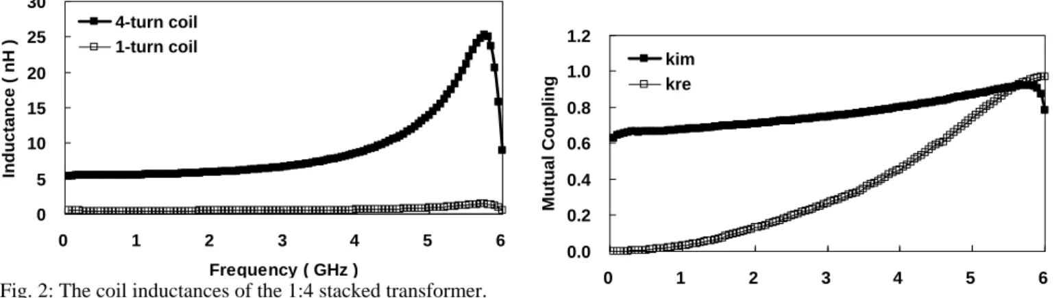
According to [2], the inductances of both the primary coil and the secondary coil can be extracted from the imaginary part of Z11 and Z22, respectively. The obtained coil inductances of the 1:4 stacked transformer are shown in Fig. 2. At low frequencies, the inductance of the 1-turn coil is around 0.5 nH while that of the 4-turn coil is around 5.3 nH. Both coils exhibit a self-resonant frequency around 6 GHz. Within the 5-GHz band, the inductance ratio of the 4-turn coil to the 1-turn coil is 15 ~ 17, which is quite close to the square of the turn ratio 4.
0 5 10 15 20 25 30
0 1 2 3 4 5 6
Frequency ( GHz )
Inductance ( nH )
4-turn coil 1-turn coil
Fig. 2: The coil inductances of the 1:4 stacked transformer.
The two coils can be evaluated by calculating their Q-factors as how we deal with inductors. The Q-factors of the two coils
are shown in Fig. 3. At 5.4 GHz, the Q-factor of the 1-turn coil is 1.7 while that of the 4-turn coil is 2.1. The maximum Q-factor of the 1-turn coil (2.4) occurs at 4.8 GHz while that of the 4-turn coil (7.0) occurs at 2.6 GHz.
0 1 2 3 4 5 6 7 8
0 1 2 3 4 5
Frequency ( GHz )
Q-factor
6 4-turn coil 1-turn coil
Fig. 3: The coil Q-factors of the 1:4 stacked transformer.
The mutual inductance and resistance between the primary coil and the secondary coil can be extracted from the imaginary part and real part of Z21 (or Z12), respectively. Then the mutual reactive (resistive) coupling factor kim (kre) can be obtained from the mutual inductance (resistance) along with the imaginary parts (real part) of Z11 and Z22 [2].
The mutual reactive and resistive coupling factors of the 1:4 stacked transformer are shown in Fig. 4, where the mutual reactive coupling factor is 0.6 ~ 0.9 and the mutual resistive coupling factor can reach 0.97 at 6 GHz, indicating a strong coupling between the two coils.
In fact, the mutual coupling factors not only depend on the interaction between the coils but also relate to the self-inductances of the coils. As shown in the Fig. 1, the metal lines connecting the transformer and the G-S pads are also part of the coils and can contribute to the coil inductances.
However, these lines can hardly cause a strong interaction between the two coils as they are relatively far from the principal part of the transformer. Therefore, the lines used to connect transformers with other elements should be as short as possible to prevent the degradation in the mutual coupling factors.
0.0 0.2 0.4 0.6 0.8 1.0 1.2
0 1 2 3 4 5
Frequency ( GHz )
Mutual Coupling
6 kim
kre
Fig. 4: Mutual reactive and resistive coupling factors of the 1:4 stacked transformer.
> REPLACE THIS LINE WITH YOUR PAPER IDENTIFICATION NUMBER (DOUBLE-CLICK HERE TO EDIT) < 3
For any two-port device, the maximum achievable power gain is defined by Gmax. Since transformers are passive elements, the absolute values of their Gmax (in dB) represent their minimum insertion losses as well as their noise figures on a condition that the impedance is matched. People even regard Gmax as a favorable choice of the figure-of-merit for a transformer [2]. The measured Gmax and S21 of the 1:4 stacked transformer are shown in Fig. 5. The 1:4 stacked transformer can deliver a moderate power gain as can be seen from the Fig.
5, where Gmax of -2.4 ~ -2.2 dB can be achieved over the 4.9 ~ 5.9 GHz band.
Fig. 6: The block diagram of the receiver front-end.
-45 -40 -35 -30 -25 -20 -15 -10 -5 0
0 1 2 3 4 5
Frequency ( GHz )
Energy Transfer ( dB )
6 Gmax S21
-20 -18 -16 -14 -12 -10
4.8 5.0 5.2 5.4 5.6 5.8
Frequency ( GHz )
S11 ( dB )
-20 -18 -16 -14 -12 -10
4.8 5.0 5.2 5.4 5.6 5.8
Frequency ( GHz )
S11 ( dB )
Fig. 5: The maximum available power gain and S21 of the 1:4 stacked transformer.
Apparently, the S21 curve lies below the Gmax curve over the entire band of observation. This is resulted from that the port impedances for both coils are not equal to 50 ohm. Therefore, it is suggested that Gmax, instead of the S21, should be used to evaluate the loss of a transformer.
Fig. 7: The measured input-return-loss (S11) of the receiver front-end.
0 10 20 30
4.8 5 5.2 5.4 5.6 5.8
Frequency ( GHz )
Gain ( dB )
III. TRANSFORMER-INTEGRATED RECEIVER FRONT-END
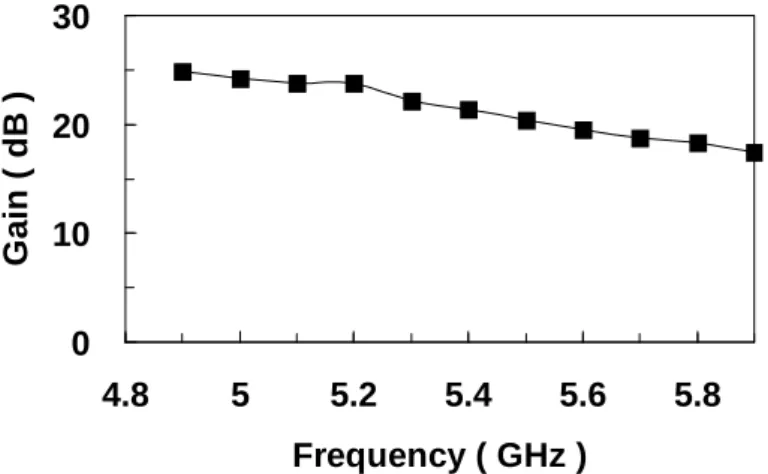
A 5-GHz receiver front-end is designed and fabricated by using 0.18-um CMOS technology. The block diagram of the receiver front-end is shown in Fig. 6. The circuit consists of a low noise amplifier [3] and a quadrature coupler [4] and two doubly balanced mixers which are based on the Gilbert cell.
The differential pair used as the transconductor in the conventional Gilbert mixer is replaced by 1:4 transformers which provide the single-ended-to-differential conversion and the voltage gain. By taking the loss and the turn ratio of the transformer into account, the voltage gain contributed by the transformer is around 10 dB in our estimation. A stacked transformer with a turn ratio of 2:2 is used to convert the single-ended 5-GHz LO signal into differential signals for doubly balanced mixers of the receiver front-end.
Fig. 8: The measured voltage gain versus input frequency of the receiver front-end.
> REPLACE THIS LINE WITH YOUR PAPER IDENTIFICATION NUMBER (DOUBLE-CLICK HERE TO EDIT) < 4
ACKNOWLEDGMENT
-120 -80 -40 0
-60 -50 -40 -30 -20 -10
Financial supports from national science council under contract number NSC 97-2221-E-011-142, chip fabrication from UMC and on-wafer measurement assistance from NDL are appreciated.
Pin ( dBm )
Pout ( dBm )
REFERENCES
0 [2
[1] J. Long, “Monolithic Transformers for Silicon RF IC Design,” IEEE J. of Solid-state Circuits, Vol. 35, No. 9, Sept. 2000.
] K. T. Ng, B. Rejaei and J. N. Burghartz, “Substrate Effects in Monolithic RF Transformers on Silicon,” IEEE T. on Microwave Theory and Techniques, Vol. 50, No. 1, pp. 377-383, Jan., 2002.
[3] H.-C. Chen, T. Wang, H.-W. Chiu, Y.-C. Yang, G.-W. Huang and S.-S.
Lu, “A 5-GHz-Band CMOS Receiver with Low LO-Self-Mixing Front-end”, accepted to be published in IEEE Transactions on Circuits and Systems I, April, 2009.
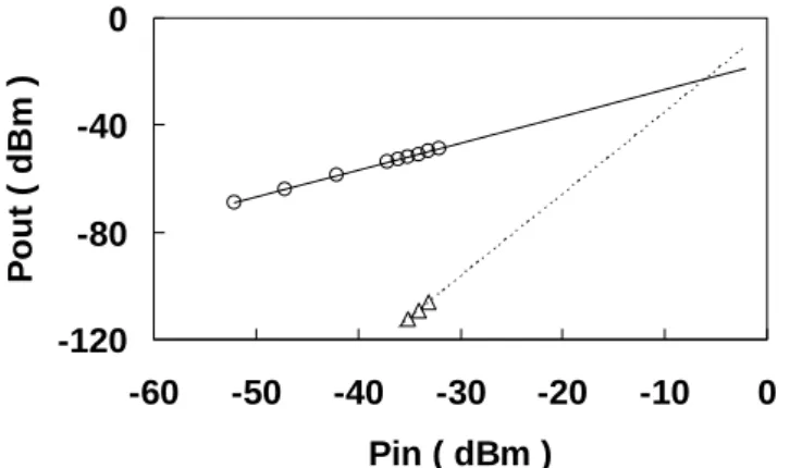
Fig. 9: The two-tone measurement result of the receiver front-end.
[4] H.-C. Chen, T. Wang and S.-S. Lu, “A 5-6 GHz 1-V LO-Self-Mixing-Free CMOS Direct-Conversion Receiver with an Integrated Quadrature Coupler,” IEEE J. of Solid-State Circuits, vol. 42, no. 9, Sept. 2007.
Fig. 10: The die photo of the receiver front-end.
LNA Mixer
IV. SUMMARY
In this work, on-chip transformers with high mutual coupling factors (~0.9) are designed and characterized for wireless integrated circuits. The application of on-chip transformers in a 5.0-GHz receiver front-end is demonstrated in 0.18-um CMOS technology. The use of transformer offers the single-to-differential conversion without nonlinear effect and hence the realized circuit presents good linearity. The receiver frond-end exhibits a voltage gain of 25.0 dB and an IIP3 of -5.9 dBm at 5.0 GHz at a power consumption of 36 mW.