國立臺灣大學電機資訊學院光電工程研究所 碩士論文
Graduate Institute of Photonics and Optoelectronics College of Electrical Engineering and Computer Science
National Taiwan University Master Thesis
以穿透式電子顯微術探討氮化物半導體奈米結構 Investigation of Nitride Semiconductor Nanostructures
with Transmission Electron Microscopy
李仁宏 Jen-Hung Li
指導教授:楊志忠 博士 Advisor: C. C. Yang, Ph.D.
中華民國九十八年七月 July, 2009
誌謝
首先感謝指導教授楊志忠博士兩年的指導與鼓勵,帶領我進入多 采多姿的光電領域,並讓我了解團體中待人處事的道理,而且提供豐 富的設備和資源使我得以完成我的研究,在此致上我由衷的感謝。
其次要感謝貴儀中心 300kv FEG TEM 操作技術人員陳學人以 及博士後研究員蔡鴻麟學長。此外,還要感謝台大光電所陳永昇學長、
張文明學長、廖哲浩學長、已畢業的台大光電所王俊凱學長在試片製 作及實驗上給我的建議,讓我可以順利完成我的論文。
接著感謝黃政傑學長、陳志諺學長、盧彥丞學長在磊晶與光學量 測方面的協助,以及蕭文裕學長在 XRD 方面的量測,還有博士後研 究員黎欣怡(Nola Li)學姊指導我英文技巧,使得這篇論文內容更加完 善,再來感謝陳永昇學長、蕭文裕學長、陳正言學長、沈坤慶學長、
呂志鋒學長、唐宗毅學長、黃政傑學長、盧彥丞學長、林政宏學長、
張文明學長、丁紹瀅學長、廖哲浩學長、陳志諺學長、謝劼同學、吳 碩彥同學、吳聲霈學弟、黃哲偉學弟、楊凱閔學弟、李俊賢學弟等等 這些實驗室的夥伴們在研究生活中相互的鼓勵與討論。
最後要感謝我的家人朋友,不管是精神還是物質上,他們給我相 當多的支持和鼓勵,讓我在遭遇挫折或者心情沮喪時還能重新站起,
最終能順利地完成碩士學位。謹以此文獻給我的父母、哥哥及女友。
摘要
本論文中的第一部份,是以高解析穿透式電子顯微鏡術,來研究 單一和雙重氮化銦鎵/氮化鎵異質結構樣品的奈米結構和光學特性。此 兩系列的樣品皆是以有機金屬化學氣相沉積法的方式來成長四片不同 厚度的氮化銦鎵層的樣品,分別是25,50,100,和200奈米。由於異質結構 所導致的應變和相分離現象,我們利用測量倒置空間圖和光激螢光的 結果來了解不同深度下的晶體品質和能隙。在掃描式電子顯微鏡的結 果圖中,我們發現當應變開始釋放時,樣品表面的粗糙度會上升。在 雙重異質結構的樣品中,由高解析穿透式電子顯微術所得到的影像,
我們可以觀察到銦滴的結構,而且發現當氮化銦鎵層的厚度下降時,
銦滴的密度也會下降。
在本論文的第二部份,我們來比較兩片不同結構的氮化銦鎵/氮
化鎵多層結構的晶體品質。我們利用測量光激螢光的結果發現氮化銦
鎵層較薄氮化鎵層較厚的樣品(8奈米-6對)有比較好的光學特性。從高
解析穿透式電子式顯微鏡的影像中也發現,(8奈米-6對)樣品的銦分佈
較均勻,而且氮化銦鎵和氮化鎵的界面較清晰。透過應力分布分佈軟
體去計算氮化銦鎵井內的平均濃度及銦原子濃度的變化範圍,再加上
能量散佈光譜儀的測量結果,我們發現在(8奈米-6對)樣品中,氮化銦
鎵井內的銦濃度的變化範圍較小。
Abstract
The objective of the proposed research uses high resolution transmission electron microscope (HRTEM) to compare the nanostructures and optical properties of single and double MOCVD-grown InGaN/GaN heterostructures as well as the nanostructures of two InGaN/GaN multi-layers of different structures.
The single and double heterostructures comprised of varying InGaN thicknesses of 25, 50, 100, and 200 nm. RSM and PL measurements demonstrated the depth-dependent crystal quality and band gap due to the effects of heterostructure-induced strain and phase separation in these samples. SEM results showed that as the strain started to relax the surface roughness rose. HRTEM results of the DH samples showed formations of indium droplets depicting a trend where the density of indium droplets decreased as the InGaN thickness decreased.
The second part of this research compared the crystal quality of two
InGaN/GaN multi-layers of different structures. PL result implied a better
optical quality in the 8nm-6P sample (thinner InGaN thickness and thicker
GaN barrier) than in the 10nm-5P sample. HRTEM results showed that the
indium distribution was more uniform and the interfaces between the
InGaN wells and GaN barriers were clearer in the 8nm-6P sample than in the 10nm-5P sample. The SSA calibrated average indium contents and indium composition fluctuation, which gave us local information about the two samples. We find that the 8nm-6P sample has a weaker indium composition fluctuation than the 10nm-5P sample based on SSA results.
EDX demonstrated the same results as SSA.
Contents
口試委員會審書 ……… I 誌謝 ……… II 中文摘要 ………III Abstract ……… IV
Chapter 1 Introduction...1
1.1 Applications of Nitride-Based Materials……….1
1.2 III-Nitride Materials Growth Issues………....2
1.2.1 Crystal Structure of III-Nitride Semiconductors………...2
1.2.2 Substrate for Nitride Epitaxy………...3
1.2.3 Defects in Nitrides………...5
1.3 Review on the Characteristics of InGaN/GaN Structures.……...6
1.3.1 Strain Effect………....……....6
1.3.2 Piezoelectric Fields………....……...7
1.3.3 Spinodal Decomposition and Phase Separation....………..9
1.4 Research Motivation and Research Problems………..11
Chapter 2 Analysis Methods………..27
2.1 Specimen Preparation of Cross-section TEM……….27
2.2 Material Analysis………30
2.2.1 High-resolution Transmission Electron Microscopy
(HRTEM)………...30
2.2.2 Energy Dispersive X-ray Spectrum (EDX)……….35
2.2.3 Strain-state Analysis (SSA)……….36
2.2.4 X-ray Diffraction (XRD)……….39
2.2.5 Scanning Electron Microscopy (SEM)………40
2.3 Optical Analysis - Photoluminescence (PL)………...41
Chapter 3 InGaN/GaN Single-heterostructures (SH) and Double-heterostructures (DH) With Various InGaN Thicknesses………..55
3.1 Sample Growth and Measurement Conditions………..….55
3.2 Strain Conditions of SH and DH Samples………..56
3.3 InGaN/GaN Single-heterostrutuctures………57
3.3.1 XRD and HRTEM Results……….57
3.3.2 SEM Results………...58
3.3.3 PL Measurements and EDX Results………..59
3.4 InGaN/GaN Double-heterostrutuctures………..60
3.4.1 XRD, HRTEM Results, and SEM Results………60
3.4.2 PL Measurements and EDX Results……….62
3.5 Discussions……….63
Chapter 4 Comparison between InGaN/GaN Multi-layer Samples under Different Growth Conditions………87
4.1 Sample Growth and Measurement Conditions………..87
4.2 PL and HRTEM Results………88
4.3 EDX and SSA Results………89
4.4 Discussions……….92
Chapter 5 Conclusions………..113
References……….115
Chapter 1 Introduction
1.1 Applications of Nitride-Based Materials
III-V nitrides have many unique properties, such as wide direct bandgap,
high-thermal conductivity, and chemical stability. These properties have made III-V
nitrides attractive in recent years. III–nitride semiconductors have been considered for
light-emitting device applications in the blue and ultraviolet wavelength ranges because
they have a very broad band gap range (see Fig 1.1.1). In fact, III–V nitride-based blue
and green light-emitting diodes (LEDs) with an InGaN/GaN multiple–quantum-well
(MQW) active region are now commercially available [1]. These nitride-based blue and
green LEDs could be used in versatile applications, such as full-color displays,
full-color indicators, and traffic lights, etc. Another application of GaN-related
compounds is in fabricating blue laser diodes (LDs) for extremely high-density optical
storage systems. Because the storage density of optical compact discs (CDs) and digital
video discs (DVDs) is inversely proportional to the square of the laser wavelength, a
four- to eight-fold increase in capacity can be realized with short–wavelength laser
diodes. As the wavelength of the light gets shorter, the focal diameter becomes smaller.
The storage density is predicted to go up from today’s 1 Gb to about 40 Gb per compact
disk when blue lasers are used.
There is great development potential for white leds in the field of lighting. Nichia
Corporation is the first company who used blue-LED chips with yellow phosphors to
make white LEDs. The common light sources today are light bulbs and fluorescent
tubes; however, they are high-energy consuming and short life time. The nitride-based
LEDs are more reliable and efficient than conventional light sources, therefore much
effort must be paid on generating white light with nitride-based LEDs.
1.2 III-Nitride Materials Growth Issues
1.2.1 Crystal Structure of III-Nitride Semiconductors
Like most other semiconductors, the atoms in the nitrides are tetrahedrally
coordinated. The s and p orbitals in the outer electron shells combine to produce hybrid
sp3 orbitals where the probability of finding an electron in a p-state is 3 times as much as finding it in an s-state. As a result, each atomic site has four nearest neighbors
occupying the vertices of a regular tetrahedron, in a manner similar to the
diamond-cubic structure.
There are three common crystal structures in nitride semiconductors: the wurtzite
(Wz), the zincblende (ZB), and the rocksalt structures. At room-temperature, the wutzite
structure is the most stable. The space group for the wurtzite structure is P63mc (C46V )
as shown in Fig. 1.2.1(a). The wurtzite structure has a hexagonal unit cell consisting of
two interpenetrating Hexagonal Close Packed (HCP) sublattices, and two lattice
constants, c and a. The parameters of the hexagonal wutzite structure GaN are a =
3.189Å (Table.1.1). For the Wz structure, the stacking sequence of the (0001) plane is
ABABAB in the <0001> direction as shown in Fig. 1.2.1(b). The space group for the
zincblende structure is F4 3m(T− 2d) as shown in Fig. 1.2.2(a). The zincblende structure has a cubic unit cell, containing four group-III elements and four nitrogen elements. The
lattice parameters of the zincblend structure GaN are a = 4.52 Å (Table.1.1). For the ZB
structure, the stacking sequence of the (111) plane is ABCABC in the <111> direction
as shown in Fig. 1.2.2(b) [2]. These lattices are polar in nature, since the anions and the
cations occupy planes that are displaced from one another along the <0001> and the
<111> directions for the hexagonal and cubic structures, respectively.
1.2.2 Substrate for Nitride Epitaxy
One of the major difficulties, which has hindered GaN research, is the lack of a
suitable substrate material that is lattice matched and thermally compatible with GaN.
There are several substrates such as ZnO, SiC, and sapphire for growing thin films of
GaN. ZnO has the wurtzite structure, and is mismatched by only 1.8% to GaN.
Unfortunately, ZnO crystals are not easy to make, and ZnO is not as thermally stable as
might be desired. Nevertheless, ZnO is important for MBE growth [3]. Another choice
of substrate is SiC because it also has a smaller lattice mismatch (3.3%) with GaN.
However, there are problems in using SiC. For example, the defect densities of the
grown samples both in bulk and surface structure are still quite high [4]. Also, the
p-type contacts and p-type dopant activation are still quite poor [5]. The high price is
another drawback of using SiC as substrate. Nowadays, sapphire is the most commonly
used substrate for epitaxy growth of nitrides. Sapphire (α-Al2O3) has a hexagonal
structure that can be expressed both as a hexagonal as well as a rhombohedral unit cell
as shown in Fig. 1.2.3. As a substrate, sapphire (α-Al2O3) is inferior to others because of
the large lattice mismatch with nitrides (14.8% with GaN and 25.4% with InN) and
significant thermal expansion difference. Despite those disadvantages, sapphire remains
the most frequently used substrate for III-nitride epitaxial growth owing to its low cost,
its stability at high temperatures, its hexagonal symmetry, and a fairly mature
technology for nitride growth on it. The orientation order of GaN films grown on
principal sapphire planes: c(basal)-plane, a-plane (112 0), and r-plane (1− 1 02) was −
studied in great detail by Electron Cyclotron Resonance-MBE (ECR-MBE). The quality
of GaN films grown directly on sapphire was very poor before the advent of buffer
layers. AlN was first used as a buffer layer by Amano and Akasaki. Nakamura et al.,
grew a GaN buffer layer on a sapphire substrate for the first time. They lowered the
substrate temperature to between 450°C and 600°C to grow the buffer layer. Then, the
substrate temperature was elevated to above 1000°C to grow the GaN films [6].
1.2.3 Defects in Nitrides
GaN epitaxial layers are usually grown on sapphire substrates. However, GaN and
sapphire have poor matching in the lattice parameter and thermal expansion coefficient,
resulting in a high density of threading dislocations (TD) (108 ~ 1010 cm-2). There are
three kinds of threading dislocations, edge, screw, and mixed types. A dislocation is a
line defect that is defined by its Burgers vector b and line direction. The Burgers vector
b describes the lattice displacement for the dislocation within the crystal. The
dislocation is an edge type if the b and dislocation are perpendicular, as shown in Fig.
1.2.4, whereas it is a screw type if these vectors are parallel, as shown in Fig. 1.2.5. A
mixed dislocation has both an edge and a screw component (see Fig 1.2.6) [7]. A
threading dislocation usually terminates with a V-shaped defect on the sample surface. It
is well–known that such dislocations act as nonradiative centers in III–V and II–VI
semiconductors [8], [9]. Hino et al. discovered threading dislocations having a
screw-component burgers vector act as strong nonradiative centers in GaN epitaxial
layers, whereas edge dislocations, which are the majority, do not as nonradiative centers
[10]. It was believed that the density of V-shape defects would be reduced if GaN
epitaxial layers were grown on GaN free–standing substrates. Generally speaking,
increasing the quantum well numbers in MQW structures or increasing the indium
contents in the QWs enhances the formation of V-shaped defects. The formation of
V-shaped defect is for strain relaxation and the reduced Ga incorporation on
the{10 11}planes, in comparison with the (0001) surface [11]. The V–shape defect
consists of three important features: (I) the initiation point at a threading dislocation
(TD), which is buried below the bottom of the open apex; (II) buried MQWs on
the{10 11} planes, pyramid walls; and (III) an open hexagonal inverted pyramid as
shown in Fig. 1.2.7. Fig. 1.2.7(a) shows the typical cross-section TEM of V-shape
defects. Fig. 1.2.7(b) shows the perspective view indicating the six sides of the open
hexagonal pyramid (defined by the{10 11}planes) and non-crystallographic plane that
terminates the side-wall quantum wells; then part (c) shows the cross-section view
indicating the open V (defined by the{1011} planes), the side-wall quantum wells, and
the inclined noncrystallographic plane that terminates the side-wall quantum wells [11].
1.3 Review on the Characteristics of InGaN/GaN Structures
1.3.1 Strain Effect
During hetero-structure growth, strain is introduced near the interface because of
the lattice mismatch between sapphire and GaN or between GaN and InN. The epilayer
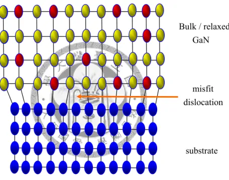
is thicker; the stored strain energy is larger. Beyond a certain thickness, known as the
critical thickness (tc), the strain energy is relaxed by forming misfit dislocations (see Fig.
1.3.1). A misfit dislocation forms at the interface between crystals of the same
orientation but different lattice parameter. The atoms at the interface adjust their
positions to give regions of good and bad registry [12]. If ae and as are lattice constants
of an epilayer (thickness t) and the substrate, respectively, when ae > as, and t < tc, the
epilayer will experience a compressive stress and hence compressive strain is built (see
Fig. 1.3.2). In this situation, a misfit strain is built in the epilayer, which is parallel to the
interface. Such a layer is called pseudomorphic strained layer. When ae < as, the epilayer
is affected by a tensile stress and hence tensile strain is produced. If t > tc, the strain is
relaxed and misfit dislocation is produced.
1.3.2 Piezoelectric Fields
Perfectly lattice matched conditions between the well and the barrier materials are
implicitly assumed in the theory. Generally speaking, lattice constants in the lateral
plane of the well and of the barrier material are different and there exist strains in one or
both of the components. The nitrides are piezoelectric materials, so the heterostructures,
including GaN/AlN, AlN/GaN, and InGaN/GaN can induce static electric fields via
piezoelectric effect [13]. Takeuchi et al. demonstrated that the piezoelectric field can
induce the quantum-confined Stark effect and plays an important role in InGaN/GaN
quantum wells. Strain caused by lattice mismatch or different thermal expansion
coefficient between the substrate and the epitaxial layers lead to piezoelectric field. The
biaxial strains also lead to the piezoelectric field along the z direction in a wurtzite
structure. This field caused the electrons and the holes to move toward opposite
directions in the well. The overlap of the electron and hole wavefunctions is reduced;
thus, the quantum confinement energy levels are different from those in the original
confinement potential. This reduction is expected to result in the decrease of the
recombination rate. In crystals with a wurtzite structure, the piezoelectric tensor is
written as:
where eij are the piezoelectric constants. The piezoelectric polarization along the z-axis,
PPE,arises as:
PPE = e33εZ+e31(εx+εy) (1.1)
0 0 0 0 e
150
0 0 0 e
150 0
e31 e31 e330 0 0
Charge neutrality condition leads to the electric field along the Z-axis, Fz , as:
Fz = -PPE /εr//εo , (1.2)
where εr// is the dielectric constant in vacuum and εo is the dielectric constant along the
z-axis. Bernardini et al. [14] have predicted that in addition to the high piezoelectric
polarization, the spontaneous polarization PSP (polarization at zero strain) cannot be
ignored in group–III nitrides. Therefore, the total polarization is the sum of the
piezoelectric and spontaneous polarization as:
P = PPE + PSP (1.3)
Several research groups have reported the values of eij as shown in Table 1.2. As
shown in Fig. 1.3.3, the macroscopic polarization in the material, comprising the active
region of the multiple quantum wells, gives rise to the net electric field perpendicular to
the plane of the well. This field, if strong enough, will induce a spatial separation of
electron and hole wavefunctions in the well. This phenomenon is also called quantum
confined Stark effect (QCSE). Hence, the wavefunction overlap decreases and the
interband recombination rate is reduced.
1.3.3 Spinodal Decomposition and Phase Separation
Spinodal decomposition is a transformation process in which there is no barrier to
nucleation. Consider a phase diagram with a miscibility gap (see Fig. 1.3.4). If an alloy
with composition X0 is treated at a high temperature T1 and then quenched to a lower
temperature T2, the composition will initially be the same everywhere and its free
energy will be G0 on the G curve. However, the alloy will immediately become unstable
because small fluctuations in composition that produce A-rich and B-rich regions will
cause the total free energy to decrease. Therefore, “up-hill” diffusion takes place until
the equilibrium compositions X1 and X2 are reached. The above process can occur for
any alloy composition where the free energy curve is concave in shape, i.e. d2G/dx2 < 0.
Therefore, the alloy must lie between the two points of inflection on the free energy
curve.
Solid phase immiscibility and phase separation in InGaN related to elastic strain
[15] have been deliberated by Stringfellow [16] and Karpov et al. [17]. According to
Stringfellow [16], the critical temperature (Tc), above which the InN-GaN system is
completely miscible is found to be near 1250 K. At a typical growth temperature of 800
ºC, the solubility of InN in GaN is calculated to be less than 6%. Stringfellow and Chen
stressed that spinodal decomposition can occur in several situations including clustering,
phase separation, and ordering. The reaction that occurs is determined by the growth
kinetics. Both thermodynamic and kinetic factors play roles in determining the degree
of order for specific epitaxial growth parameters and on which planes the compositional
modulations occur. The thermodynamic driving force leads to a reduction of the
microscopic strain energy due to stretching and bending of the bonds. Certain ordered
alloys have lower energies than a disordered alloy. The formation of two separate,
incoherent phases will result in even lower energy configuration. However, this is
prevented in practice by the coherency strain energy inherent in the initial stages of
phase separation. The kinetic effect plays an important role in growth parameters such
as the growth temperature, growth rate and substrate orientation. Behbehani et al. [18]
reported on the existence of simultaneous phase separation and ordering of InxGa1-xN
samples with x > 0.25. Karpov et al. [17] used the Valence Force Field (VFF)
approximation for the analysis of lattice distortion and determination of the interaction
energy of GaN and InN in InGaN ternary compounds.
1.4 Research Motivation and Research Problems
The (Al, Ga, In)N material system has been extensively investigated due to their
potential applications in light-emitting diodes (LEDs), laser diodes, and photodetectors.
[19] In recent years, InGaN alloys emerge as a new solar cell material system due to
their characteristics of high absorption, broad spectral coverage, and radiation hardness.
InGaN is particularly useful for converting sunlight in the visible range into electrical
power. For this purpose, the growth of high-quality InGaN thin films with indium
content higher than 20 % becomes important [20]. However, because of the large lattice
mismatch (11 %) between GaN and InN, phase separation occurs when the InGaN
thickness is larger than its critical thickness, which is smaller than 60 nm for indium
content higher than 20% [21]. Within the critical thickness, under the
heterostructure-induced strain, indium incorporation is relatively lower leading to
lower-indium growth. Beyond the critical thickness, relaxed strain leads to more
significant indium incorporation. Although an InGaN thin film has been widely grown,
its indium composition distribution and hence band gap distribution are not well
understood yet. In particular, the possible indium droplet formed in phase separation
when a p-type GaN cap layer of high-temperature growth is added to form a p-i-n
structure has not been well studied.
In this research, we present our measurement results of cross sectional
transmission electron microscopy (TEM), scanning electron microscopy (SEM), energy
dispersive X-ray spectrum (EDX), X-ray diffraction (XRD), and photoluminescence
(PL) on InGaN/GaN single-heterostructures (SH) and double-heterostructures (DH)
with various InGaN thicknesses.
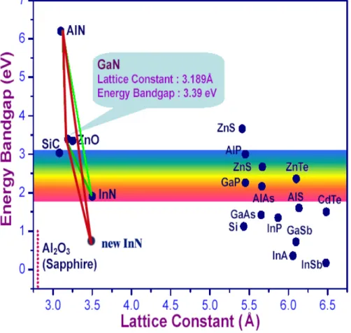
Fig. 1.1.1 Energy band gap versus lattice constant in II-VI and III-V
compound semiconductors.
http://kottan-labs.bgsu.edu/teaching/workshop2001/chapter5.htm Fig. 1.2.1(a) Hexagonal Wurtzite structure of GaN.
Fig. 1.2.1(b) Crystalline layer sequences of hexagonal Wurtzite structure.
http://kottan-labs.bgsu.edu/teaching/workshop2001/chapter5.htm Fig. 1.2.2(a) Cubic Zincblende structure of GaN.
Fig. 1.2.2(b) Crystalline layer sequences of cubic Zincblende structure.
Fig. 1.2.3 Crystal lattice of sapphire.
Fig. 1.3.2 Edge Dislocation.
Fig. 1.2.4 Edge Dislocation.
Fig. 1.2.5 Screw Dislocation.
Fig. 1.2.6 Mixed Dislocation.
Fig.1.2.7(a) Typical cross-section TEM of V-shaped defects.
Fig. 1.2.7(b) Perspective view and (c) cross-section view of V-shaped
defects.
http://www.sp.phy.cam.ac.uk/~dp350/Misfit.html
Fig. 1.3.1 Schematic illustraction of a misfit dislocation formed during epitaxial growth.
Bulk / relaxed GaN
misfit dislocation
substrate
Fig.1.3.2 Compressive and tensile strains
Tensile strainsubstrate epilayer
substrate epilayer
Compressive strain
substrate substrate
epilayer
epilayer
http://nsr.mij.mrs.org/3/31/tnfigures.html
Fig. 1.3.3 Schematic of the strain induced along the growth direction, the resulting piezoelectric charges, and the bandstructure of a GaN-GaInN-GaN heterostructure.
Growth surface GaN
Sapphire GaN
z E- Field GaInN
CB
VB
Growth dirtection 0 z
εzz
z Nfix
Potential
Fig. 1.3.4 A phase diagram with a miscibility gap.
Table 1.1 The basic parameters of InN, GaN, and AlN wurtzite structures.
Parameter Units GaN AlN InN
Lattice constant, c Α o 5.186 4.982 5.693
Lattice constant, a Α o 3.189 3.112 3.533
Bandgap energy, Eg eV 3.39 6.2 0.76
Effective electron mass, me mo
0.19(∥) 0.17(⊥)
0.33(∥) 0.25(⊥)
0.11(∥) 0.10(⊥) Effective heavy hole mass, mhh mo
1.76(∥) 1.61(⊥)
3.53(∥) 10.42(⊥)
1.56(∥) 1.68(⊥) Effective light hole mass, mhh mo
1.76(∥) 0.14(⊥)
3.53(∥) 0.24(⊥)
1.56(∥) 0.11(⊥) Piezoelectric constant, e31 C/m2 -0.33 -0.48 -0.57
Piezoelectric constant, e33 C/m2 0.65 1.55 0.97
Spontaneous polarization, P∥ C/m2 -0.029 -0.081 -0.032 Radiative recombination coefficient cm3/s 4.7×10⁻¹¹ 1.8×10⁻¹¹ 5.2×10⁻¹¹
Refractive index at 555nm 2.4 2.1 2.8
Absorption coefficient at the photon
Energy hυ~Eg 105cm-1 1 3 0.4
Table 1.2 Piezoelectric constants and spontaneous polarization for III-nitrides.
ZB WZ Reference e14 peqz e33 e31 e15 BN
Shimada et al. (1998) Calc -0.64 - -0.85 0.27 - AlN
Tsubouchi and Mikpshiba (1985) Exp. - - 1.55 -0.58 - Davydov and Tikhonov (1996) Clac 0.67 - - - - Bernardini et al. (1997) Clac - -0.081 1.46 -0.60 - Shimada et al. (1998) Clac 0.59 - 1.29 -0.38 -
GaN
O’clock and Duffy (1973) Exp. 0.6 - - - - Bykhovski et al. (1996) Exp. 0.375 - 0.43 -0.22 -0.22 Davydov and Tikhonov(1996) Clac 0.68 - - - - Bernardini et al. (1997) Clac - -0.029 0.73 -0.49 - Shimada et al. (1998) Clac 0.50 - 0.63 -0.32 -
InN
Bernardini et al. (1997) Clac - -0.032 0.97 -0.57 -
Chapter 2
Analysis Method
This chapter will describe the methods used to analyze our samples including
materials and optical analysis methods. High resolution transmission electron
microscopy (HRTEM), strain state analysis (SSA), energy dispersive X-ray spectrum
(EDX), x-ray diffraction (XRD), and scanning electron microscopy (SEM) are used to
analyze material properties. Photoluminescence (PL) is used to analyze the optical
properties.
2.1 Specimen Preparation of Cross-section TEM
The objective of TEM sample preparation is to create an electron transparent
region containing the features of interest without contamination and artifacts. There are
many different methods to make TEM specimen. Among them, only three types of
techniques are commonly used, including the dimpling and ion milling technique, the
focused ion beam technique, and the wedge technique. The dimpling technique works
well for the blanket films, large features, and repeated patterns. However, it provides
smaller thin areas and is difficult to target to a special feature. The focused ion beam
technique offers a reliable method to make high precision cross-sections of the specific
area. However, this method provides a very limited area of view and is easy to introduce
damages. The wedge technique provides highest flexibility over other techniques. It can
be used to make plan view, regular cross-section specimen and precision cross-section
specimens. We can thin the sample down to less than 1 μm by pure mechanical
polishing. More importantly, the electron transparent area can be as large as millimeters.
We will explain the details about this technique since all TEM specimens used for this
research are made by the wedge technique. Several steps are as follows:
1. The first step is to have the wafer sectioned into rectangular slabs that are at least 3
mm in width and about 10 mm in length, as shown in Fig. 2.1.1(a). To do this, a
diamond wafering saw or a diamond pen can be used. The former method yields
equal-sized pieces, which are easier to handle. However, it is more time consuming.
2. Next, we need to thoroughly clean and degrease the slabs. This is best done by
ultrasonically scrubbing them in acetone and then in Freon. A cotton swab may be
used to gently remove any persistent surface contaminants. The required number of
sample slabs depends on their thickness. Generally speaking, we need two pieces of
sample slabs and two pieces of silicon.
3. We choose G1-epoxy to glue the slabs as shown in Fig. 2.1.1(b). There are three
main advantages of this glue that make it particularly suitable for this application: it
is very strong; it is very thin when properly applied (~2000 Å), and it can be ion
milled at about the same rate as silicon. Furthermore, it is impervious to the attack
of any solvent once it is set. The main drawback is that it needs to be thermoset
under pressure. To accomplish this step, a small vise is used that can be heated on a
hotplate (see Fig. 2.1.2). The two pieces of sample slabs having the thin films or
interfaces of interest must be in the center and the polished faces of these two pieces
thus face each other. Then, the sample is mounted onto the polisher, as shown in Fig.
2.1.1(c).
4. After specimen mounting, the polisher is placed on lapping films and the specimens
are wet polished using progressively finer grit diamond lapping films (30, 9, 6, 3, 1,
0.5 and 0.1 μm, respectively) for coarse polishing. The thickness of the specimen
are less than 1.5 mm after the first side polishing. The specimen will easily fall off
from the polisher during the second side polishing. The wedge angle was set at
about 0.4°. It is very important to remove any contamination or particles from the
mounting surface.
5. The polished surface is attached to the polisher using a small amount of super glue.
Sufficient super glue is used to surround the edges of the specimen to provide
certain mechanical stability during processing and to protect the specimen from the
risk of film delamination.
6. After curing the super glue, the specimens are wet polished to the desired thickness
using the same diamond lapping films in the same order as described in the first side
polishing. The specimen is checked frequently to ensure that it is polished
sufficiently thin during the last four polishing steps (3, 1, 0.5 and 0.1 μm). It is
difficult to determine whether the specimen is sufficiently polished since the
GaN/sapphire specimen is transparent. Consequently, the specimen is checked by
observing the color of silicon in transmission using an optical microscope.
7. After polishing, the specimen is removed from the polisher by soaking in acetone
and mounted onto a 2×1 mm slotted TEM grid using epoxy as shown in Fig.
2.1.1(d).
8. Then, we can have the specimen be milled by argon-ion gas for several minutes (see
Fig. 2.1.1(e).
2.2 Material Analysis
2.2.1 High-resolution Transmission Electron Microscopy (HRTEM)
Transmission electron microscopy (TEM) is probably the most important and
widely used characterization tool to study the nano-structrual characteristics of materials.
The basic reason for utilizing the electron microscopy is its superior resolution,
resulting from very small wavelengths as compared to other forms of radiation (light,
X-rays, neutrons). The resolution is given by the Rayleigh formula, which is derived by
considering the maximum angle of electron scattering, α, which can pass through the
objective lens. This formula is
R=0.61λ/α (2.1)
Where R is the size of the resolved object, λ is the wavelength, and α is identical to the
effective aperture of the objective lens. Equation (2.1) is the classic Rayleigh criterion
for resolution in light optics.
A cutaway diagram of the TEM is shown in Fig. 2.2.1. In a conventional TEM, a
thin specimen is irradiated with an electron beam of uniform current density; the
electron energy is in the range 60-150 keV (usually around 100 keV) or 200 keV-300
MeV in the case of intermediate or high-voltage electron microscopy. Electrons are
emitted in the electron gun by thermionic emission from tungsten hairpin cathodes or
LaB6 rods or by field emission from pointed tungsten filaments. The letter is used when
high gun brightness is needed. A two-stage condenser-lens system permits variation of
the illumination aperture and the area of the specimen illuminated. The electron
intensity distribution behind the specimen is imaged with a three- or four-stage lens
system, onto a fluorescent screen. The image can be recorded by direct exposure of a
photographic emulsion inside the vacuum or digitally by CCD or TV cameras.
Figure 2.2.2 illustrates the principal results of electron scattering by a sample and,
as a result, the principal sources of information that can be obtained. The operating
modes are as follows: transmission electron microscopy (TEM), scanning electron
microscopy (SEM), scanning transmission electron microscopy (STEM), and
microanalysis (by X-ray and/or energy loss analysis or Auger analysis of surfaces).
The imaging system of a TEM consists of at least three lenses (Fig. 2.2.3): the
objective lens, the intermediate lens and the projector lens. The intermediate lens can
magnify the first intermediate image, which is formed just in front of this lens (Fig.
2.2.3(a)). An image is made with only those electrons that have been diffracted by a
specific angle by positioning an objective aperture at a specific location in the back
focal plane. This defines two imaging modes.
● When the objective aperture is positioned to pass only the transmitted (undiffracted) electrons, a bright-field (BF) image is formed.
● When the objective aperture is positioned to pass only some diffracted electrons, a dark-field (DF) image is formed. (The particular diffraction should be specified.)
The intermediate lens can also magnify the first diffraction pattern, which is formed in
the focal plane of the objective lens (Fig. 2.2.3(b)). In many microscopes, an additional
diffraction lens is inserted between the objective and intermediate lenses to image the
diffraction pattern and to enable the magnification to be varied in the range 102 to 106.
The transmission electron microscopes used in this study are JEOL 100CX II and
Philips Tecnai F30 field-emission electron microscope. The JEOL 100CX II is equipped
with a tungsten electron source and operates at 100kV accelerating voltage. The
magnification range is from 500x to 300,000x and the lattice resolution is 0.2 nm (point
resolution 0.45nm). The Philips Tecnai F30 field-emission electron microscope is
equipped with a field emission gun (FEG) and operates at 300kV accelerating voltage.
The magnification range is from 60x to 1,000,000x and the lattice resolution is 0.10nm
(point resolution 0.20nm).
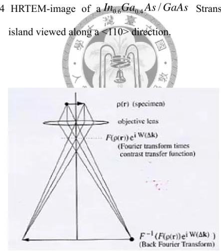
Bright-field and dark-field techniques cannot be used to form high resolution
TEM images of columns of atoms in Fig. 2.2.4. The diffracted wave, in this case an
electron wavefunction, is the Fourier transform of the scattering factor distribution in
the material, ρ(r). The shape of ρ(r) tracks the atom distribution in the material. High
resolution images are best understood in terms of Fourier transforms. We use the
notation, F(ρ(r)), to represent the Fourier transform of the distribution of atoms in the
specimen, ρ(r):
∫
−+∞∞ −Δ⋅= r e d r
r
F ( ) i kr 3
2 )) 1 (
(
ρ
ρ π
(2.2)The Fourier transform is a function of Δk, a diffraction vector. With dimensions of
inverse length, the vector Δk can account for periodicities in the specimen. Recall that a
smooth function, ρ(r), which has a large extent in r, has a Fourier transform that is
nonzero only for small values of Δk. On the other hand, a function ρ(r) that has short
periodicities has a Fourier transform containing some large Δk vectors. Fig. 2.2.5 shows
how Fourier transforms of the diffracted electron waves correspond to the specimen, the
back focal plane of the objective lens, and the image plane. An objective aperture in the
back focal plane of the objective lens will truncate the Fourier transform of the
specimen. An image formed with a small range of k-vectors can include only long-range
spatial features. For an objective aperture that selects a range, δk, the smallest spatial
features in the image are approximately x, where:△
x=2π/δk
△ (2.3)
To resolve atomic periodicities, we need an aperture that incorporates a range, δk 2π/d, ≒
where d is the atomic separation. This, however, is the typical separation of the first
diffraction spot from the transmitted beam. A much smaller aperture is used in
bright-field and dark-field imaging to collect electrons that have all beam diffracted by
the same angle. The consequent truncation in k-space means that the conventional
bright-field and dark-field modes of TEM imaging cannot produce high resolution
images. In fact, making a high resolution image requires that we use an objective
aperture large enough to include both the transmitted beam and at least one diffracted
beam. The transmitted (“forward-scattered”) beam is required to provide a reference
phase of the electron wavefront. High resolution images are in fact interference patterns
formed from the phase relationships of diffracted beams.
2.2.2 Energy Dispersive X-ray Spectrum (EDX)
Sample composition was examined by EDX. Fig. 2.2.6 shows the interaction of a
beam electron with an inner-shell resulting in an excited state with a vacancy in the
electron shell. An electron transition will come up from an outer shell to fill this vacancy.
The transition involves a change in energy, and the energy releases from the atom.
While the energy of the emitted x-ray is related to the difference in energy between the
levels of the atom, it can be ascribed as a characteristic x-ray. As in the TEM
measurements, we can determine the composition of our samples according to the
detected x-ray.
An EDX system is in Fig. 2.2.7. The computer controls three parts to carry out
any data processing. First, it controls whether the detector is on or off. Ideally, we want
to process one incoming x-ray at a time, so the detector is switched off while an x-ray
signal is detected. Second, the computer governs the processing electronics, setting the
time required to analyze the x-ray signal and assigning the signal to the correct channel
in the display screen. Third, the computer software manages both the calibration of the
spectrum readout on the screen and all the alpha-numeric, which tells us the conditions
under which the spectrum was acquired.
2.2.3 Strain-state Analysis (SSA)
Composition fluctuations in InGaN were recognized a number of years ago to
significantly determine the properties of devices fabricated on the basis of InGaN/GaN
heterostructures. It is therefore of considerable interest to study quantitatively the In
distribution of InGaN and the spatial dimension of compositional fluctuations. For this
reason, a strain-state analysis (SSA) technique has been developed, which was used to
evaluate the composition of InGaN.
Strain-state analysis (SSA) is a technique based on HRTEM lattice fringe images.
Lattice fringe images are taken under two-beam conditions by only exciting the (0000)
and (0002) beams, which is possible with a minimum number of other excited beams by
tilting the sample about 5° out of the [1-100]-zone axis along the [11-20] direction. The
images are taken with an objective aperture containing the transmitted and the (0002)
beams. Instead of using a zone-axis HRTEM image, where typically at least nine beams
are used to form an image along the [11-20]- or [1-100]-zone axes, two-beam conditions
simplify considerably the image formation process. The interference of only two beams
leads to a fringe image. The apparent loss of resolution along the (0002) fringes
compared to a conventional zone-axis image does not present a problem because only
the distances between the (0002) fringes need to be measured. This can be achieved by
carrying out closely spaced line scans.
An example for a lattice fringe image is displayed in Fig. 2.2.8(a) where a thin
InGaN QW is embedded in GaN. The distances between the (0002) planes d0002 are
measured by detecting the intensity maximum positions of the bright fringes by line
scans along the [0001] direction (white lines in Fig. 2.2.8(b)).
The composition evaluation is based on a rather simple principle by assuming that
the lattice parameter of a ternary compound, e.g. InGaN with a lattice parameter dInGaN,
is linearly dependent on the In concentration xIn.
Vegard’s law: dInGaN = dGaN + xIn(dInN-dGaN) (2.4)
InGaN is a system that is well suited for composition analysis on the basis of Eq. (2.4)
because the lattice parameter mismatch between InN and GaN is 10%. The local In
concentration is deduced from Vegard’s law by Eq. (2.5) taking into account the strain
state of the InGaN layer,
(
1)
1 1 1
. 0
+ −
= n
c
In d
K
x f (2.5)
098 .
. 0
0 = − =
GaN GaN In
c d
d f d
r j
n d
d =d
The values for dGaN and dInN are dGaN = 0.5186nm and dInN=0.5693nm. A reference
(0002) distance dr can be measured in an area of known lattice parameter, e.g. in the
relaxed GaN buffer layer. The unknown (0002)-plane distances dj in the InGaN are
normalized with dr yielding dn=dj/dr. The factor K results from the tetragonal distortion
of the InGaN lattice in strained layers. Two cases for the tetragonal distortion have to be
distinguished for TEM cross-section samples whose thickness for HRTEM imaging can
be as low as a few nanometers. A complete tetragonal distortion occurs for thick
samples (“thick foil approximation”). In contrast, the tetragonal distortion can be
completely relaxed along the electron beam direction for very thin samples (“thin foil
approximation”). The factors K, which depend on the elastic constants cij and on the
surface normal of the cross-section sample (in this case close to the [1-100] direction)
are given by Eqs. (2.6) and (2.7),
⎟⎟⎠
⎜⎜ ⎞
⎝
⎛
−
− −
=
=
2 13 33 11
2 13 33 12 33
13 33 13
1 2
c c c
c c c c
K c
c K c
thin thick
The values Kthick=0.55±0.0667 and Kthin=0.19±0.035 are almost independent of the In
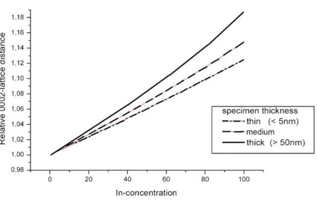
concentration [1]. Figure 2.2.9 shows the influence of the relaxation state on the
normalized lattice parameters dn, i.e. the ratio between the InGaN and the GaN c-lattice
parameters, plotted as a function of the In concentration.
In conclusion, we can use SSA technique to analyze InGaN/GaN (0002) lattice
fringe image to get the distances between the (0002) planes d0002. Then, we consider the
sample thickness and the elastic relaxation. Finally, we can get In composition of InGaN
QW. For a more detailed procedure for SSA, see Ref. [2] [3].
(2.6)
(2.7)
2.2.4 X-Ray Diffraction (XRD)
X-ray diffraction is a nondestructive technique for determining structural defects.
In a diffraction experiment, the incident waves must have wavelengths comparable to
the spacing between atoms. Consider a perfect crystal arranged to diffraction
monochromatic X-rays of wavelength λ from lattice planes spaced d and the X-rays are
incident on the sample at an angle θ (see Fig. 2.2.10). The primary beam is absorbed by
or transmitted through the sample and only the diffracted beam can be detected by the
detector. The diffracted beam emerges at twice the Bragg angle θB defined by
sin (1 )
B 2
d
θ = − λ (2.8)
Eq. (2.8) no longer applies simultaneously to the perfect and the distorted regions
if the lattice spacing or lattice plane orientation vary locally due to structural defect.
In a diffraction experiment, we use a known λ and a measurement θ to obtain
values of d/n for the sample. The slow rotation of the sample about its axis virtually
ensures. The X-ray diffraction experimental setup is shown in Fig. 2.2.11. In this
experiment, XRD measurements are carried out using Cu Kα1 (0.1542 nm) radiation,
monochromated by the (111) reflection of a Ge single crystal. The sample and the X-ray
detector are separated by 770 nm to eliminate any parasitic scattering of photons. The
coherence length and strain are measured by the traditional 2θ-θ scan.
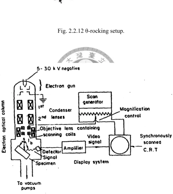
As for the θ-rocking scan (see Fig. 2.2.12), the X-ray beam intensity scattered
from the sample is recorded while the sample is scanned through a reciprocal lattice
point (rotation around a Bragg angle). The experimental rocking curves show several
features that are related to the particular structural properties of the sample. One can
characterize the strain fields completely and determine all the strain tensor elements of
the distorted unit cell of the material by recording rocking curves in the vicinity of
different reciprocal lattice points. Measurements carried out in symmetrical diffraction
geometry monitor the strain fields along the growth direction, while rocking curves
recorded in asymmetrical diffraction geometry are also sensitive to the in-plane strain.
Using the result of θ-rocking scan, we can know the distribution of crystal direction and
the scattered degree in the material.
2.2.5 Scanning Electron Microscopy (SEM)
Scanning electron microscope (SEM) techniques provide measurements with a
micron scale resolution. Therefore, we can determine defect microstructures, threading
dislocations, plane-view, cross-section images and local values of physical properties.
The term micro-characterization has come into use to emphasize this dual characteristic
of SEM. SEM is powerful and versatile because (a) it has six modes of operation, which
provide information about many different groups of properties of solid objects and (b)
the information is obtained essentially as electrical signals suitable for electronic data
processing to provide quantitative values of many different properties as well as for
presentation in various types of micrographs. The SEM is composed of two sub-systems,
shown in Fig. 2.2.13.
2.3 Optical Analysis - Photoluminescence (PL)
Photoluminescence (PL) measurement is a very powerful tool in the assessment
of optical properties of semiconductors because of its sensitivity, convenience, and
non-destructive process. It provides a direct way to detect and identify energy-state
distribution in materials.
A laser beam of an appropriate wavelength excites the electrons from the valence
band to the conduction band and creates electron-hole pairs. When the electron-hole
pairs recombine, the energy is released. There are two forms of released energy
including nonradiative recombination and radiative recombination. Only radiative
recombination can be detected. In our study, we performed temperature-dependent PL
measurements to investigate the recombination mechanisms, which originates from
spinodal decomposition and indium aggregated structures in InGaN well regions.
The standard PL experimental set up is shown in Fig. 2.3.1. The 325 nm-line of a
35 mW He-Cd laser is used for excitation. The samples to be measured were placed in a
cryostat for constant-temperature measurements at 300 K. PL photons from samples
were collected with a lens and guided into a monochrometor through a fiber bundle. The
PL signals were monitored with a lock-in amplifier.
Fig. 2.1.1 Flow path of sample preparation.
Fig. 2.1.2 Schematic drawing of the small vise.
Fig. 2.2.1 A cutaway diagram of the transmission electron microscopy.
Fig. 2.2.2 Signal generated when a high-energy beam of electrons
interacts with a thin specimen. Most of these signals can be
detected in different types of TEM. The directions shown for
each signal do not always represent the physical direction of the
signal but indicate, in a relative manner, where the signal is
strongest or where it is detected.
Fig. 2.2.3 Ray diagram for a transmission electron microscope in (a) the
bright-field mode and (b) selected-area electron diffraction
(SAED) mode.
Fig. 2.2.4 HRTEM-image of a In Ga As GaAs
0.6 0.4/ Stranski-Krastanow island viewed along a <110> direction.
Fig. 2.2.5 Fourier transforms and planes of a ray diagram. The function
e
iW(△k)accounts for the characteristics in the objective lens.
Fig. 2.2.6 The diagram of X-ray (K-lines and L-lines).
Fig. 2.2.7 Schematic process for the energy dispersive X-ray spectrum
(EDX).
(a)
(b)
Fig. 2.2.8(a) (0002) lattice fringe image of a GaN/InGaN/GaN QW.
structure;
(b) Line scans are used to determine the intensity maximum
positions of the fringes. The size of an image unit cell is
indicated by the black rectangle.
Fig. 2.2.9 Influence of the relaxation state on the normalized lattice parameters d
nplotted as a function of the In concentration.
Biaxial strain state for a “thick” sample (solid line) and
monoaxial strain state for a “thin” sample (dashed line).
Fig. 2.2.10 Illustration of the Bragg condition.
Fig. 2.2.11 X-ray diffraction setup (2θ-θ).
Fig. 2.2.12 θ-rocking setup.
Fig. 2.2.13 SEM system, consisting of an electron optical column and a
detection-amplification-display system.
He-Cd Laser (325nm)
Chopper
PMT
Cryostat
Fiber Bundle
Lock-in Amplifier PC
Monochromator
Sample
Fig. 2.3.1 The experiment setup for PL measurement.
Chapter 3
InGaN/GaN Single-heterostructures (SH) and Double-heterostructures (DH) With Various InGaN Thicknesses
In this chapter, we will compare the nanostructures and optical properties of two
series of sample including single-heterostructures (SH) and double-heterostructures
(DH) with various InGaN thicknesses of 25, 50, 100, and 200 nm. All samples were
grown under the same growth conditions with an additional GaN caplayer grown at high
temperature for the DH samples.
3.1 Sample Growth and Measurement Conditions
All samples were grown by metalorganic chemical vapor deposition (MOCVD).
The InGaN/GaN SH samples were prepared in the following manner. First, a 2~3 μm
undoped-GaN layer was grown on (0001) c-plane sapphire substrate at 1080 °C. Then,
an InGaN layer was grown at a growth temperature of 700 oC. Various InGaN layer
thicknesses were implemented at 25, 50, 100, and 200 nm. The DH samples were grown
under the same conditions as those of the SH samples with an additional final GaN layer
of 120 nm thickness grown at 920 oC. The detailed structures of these two series sample
are shown in Figs. 3.1.1.
X-ray diffraction (XRD) was used to measure reciprocal space mapping (RSM) in
order to understand the strain condition in a sample. Indium content distribution can be
calibrated based on the strain information. Omega-2theta ( ω -2 θ ) scans were
performed to understand the composition in a sample. Indium droplets can be detected
based on the corresponding peak position in the ω-2θ diagram. Scanning electron
microscope (SEM) measurements were performed to compare the roughness of the SH
and DH samples of different thicknesses. Energy dispersive X-ray spectrum (EDX) was
measured to obtain the elemental distribution in a sample. The calibrated indium
contents were confirmed by photoluminescence (PL) measurements by exciting from
the top and bottom sides of the sample. Transmission electron microscopy (TEM)
measurements were then performed to observe the indium droplets within the InGaN
films of the DH samples.
3.2 Strain Conditions of SH and DH Samples
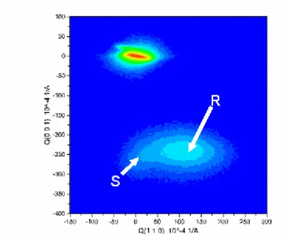
An example of RSM results is shown in Fig. 3.2.1. Figure 3.2.1(a) shows the
RSM plot of an SH sample with the InGaN layer thickness at 200 nm and growth
temperature of 700 oC. The bright spot at the upper-left corner represents GaN in the
sample. A spot directly below the GaN spot is a fully strained material. A deviation from
the perpendicular demonstrates the amount of strain or relaxation in the material. The
horizontally extended spot in the lower half portion stands for InGaN of a certain strain
and indium distribution. A point (labeled by S) corresponds to a fully strained InGaN
composition. A second point (labeled by R) corresponds to a fully relaxed InGaN
composition. The trace from point S to R corresponds to the growth process of the
InGaN layer from the fully strained condition (within the critical thickness) to a fully
relaxed condition. In the early growth stage during the strained condition, the indium
incorporation is low such that only 19 % indium composition is achieved. Indium
content is increased to 27 % as strain is gradually relaxed. The RSM plot of a DH
sample corresponding to the structure and growth condition of the sample is shown in
Fig. 3.2.1(b). Here, one can see that almost the whole InGaN layer is fully strained. This
is so because the InGaN layer is compressively strained by GaN from its top and
bottom.
3.3 InGaN/GaN Single-heterostrutuctures
3.3.1 XRD and HRTEM Results
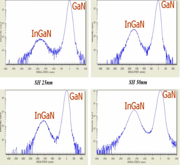
Figure 3.3.1 shows XRD ( ω -2 θ scans) of SH samples with different
thicknesses, including 25, 50, 100, and 200 nm. Here, only the GaN and InGaN peaks
are seen (labeled in Fig. 3.3.1). No phase separation is seen near the InGaN peak.
HRTEM images of the four SH samples are shown in Fig. 3.3.2. Here, we can see the
general structures of the four samples. Figure 3.3.2(a) shows the cross-section HRTEM
image of SH 25nm. The arrow indicates the direction of (0001) from the substrate. The
G1 glue and InGaN thin film can be seen. The different atomic masses, indium (49) is
higher than that of gallium (31), causing the contrast in an HRTEM image. The heavier
atom results in a darker color in an image. Figures 3.3.2(b), (c), and (d) show the
cross-section HRTEM images of samples SH 50, 100, and 200 nm, respectively. Then,
we compare the roughness of the above-mentioned four SH samples. We find that the
InGaN layer roughness increases with an increase of InGaN thickness. SEM results will
show clearer evidence.
3.3.2 SEM Results
SEM studies were performed to more clearly demonstrate the surface roughness
of these four SH samples of different thicknesses. The plane-view SEM images of
samples SH 25, 50, 100, and 200 nm are shown in Figs. 3.3.3(a), (b), (c), and (d),
respectively. We can observe the surface roughness on the plane-view SEM image. They
are quite different. The 200nm sample clearly shows valleys and peaks over the surface.
The images show that the surface becomes smoother as the sample thickness decreases.
As we discussed in section 3.2, RSM plot (Fig. 3.2.1 (a)) of sample SH 200 nm showed
the growth process of an InGaN layer from a fully strained condition (within the critical
thickness) to a fully relaxed condition. So, when the strain starts to relax, surface
roughness will rise. We have directly confirmed that when the thickness of InGaN layer
increases, the roughness also rises.
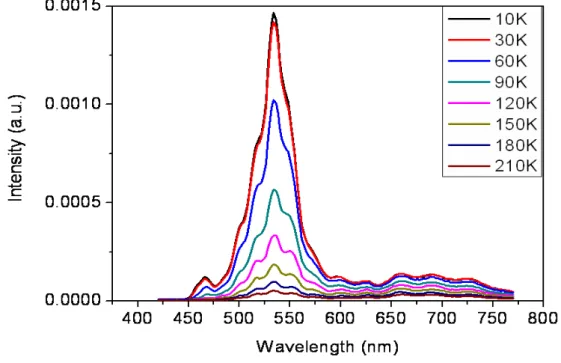
3.3.3 PL Measurements and EDX Results
PL measurements were excited from the top (the film side) and bottom (the
polished backside) of the samples from 10 through 210 K, as shown in Figs. 3.3.4(a)
and (b). Figure 3.3.4(a) and (b) show the PL measurement results of the most upper and
lower portions of the InGaN layers, respectively, because the penetration depth of the
excitation UV laser (390 nm) in InGaN is only around 100 nm. From Figs. 3.3.4(a) and
(b), one can see that the upper (lower) InGaN layer mainly emits green (blue) light
around 520 (460) nm even though a small shoulder can be seen in the blue (green) range.
These PL measurements are consistent with the RSM results above, i.e., the upper
(lower) InGaN layer has higher (lower) indium content.
EDX was used to estimate indium content for matching the above PL
measurements. Here, we can only obtain the relative indium content because of the
uncertain incident angle of the electron beam. Figure 3.3.5(a) shows the direction (red
arrow) of the eight points measured by EDX in SH 200 nm. The white arrow indicates
the direction of (0001) from the substrate. Then, the data at the eight points were used to
draw a diagram for the relative indium content versus points (as shown in Fig. 3.3.5(b)).
Here, we find that indium content increases with height. However, the indium contents
of the last three points decrease. This result might be due to indium escape under the
thermal treatment of the SH samples after growth. The thermal treatment of SH samples
means that right after closing the MO sources, the samples are still in an environment of
hydride gases and high temperature for a few more minutes. This may lead to InGaN
decomposition from the upper most surface. Generally, the EDX data are consistent
with the above PL measurements.
3.4 InGaN/GaN Double-heterostrutuctures
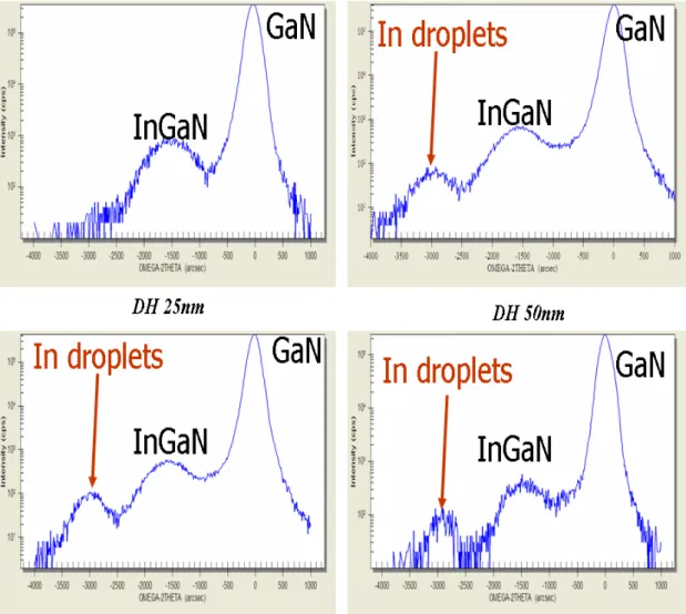
3.4.1 XRD, HRTEM, and SEM Results
In this section, we compare the different properties between SH and DH samples.
XRD (ω-2θ scan) of DH samples of different thicknesses, including 25, 50, 100, and
200 nm are shown in Fig. 3.4.1. Here, we can see additional peaks besides GaN and
main InGaN peak showing the occurrence of phase separation in the InGaN layer
(labeled in Fig. 3.4.1). Hartono et al [1] attempted to grow InN directly on GaN, which
resulted in indium droplet formation. They showed that XRD and the peak for indium
droplets were consistent with our data. It is possible that indium droplets have been