Determination of stress-optical and thermal-optical coefficients
of Nb
2O
5thin film material
Tei-Chen Chena兲
Department of Mechanical Engineering, National Cheng Kung University, Tainan 701, Taiwan Ching-Jiung Chu
Department of Mechanical Engineering, Far East Technology College, No. 49, Chung Hua Road, Hsin-Shi, Tainan County 744, Taiwan
Chang-Hsien Ho and Chung-Chen Wu
Department of Mechanical Engineering, National Cheng Kung University, Tainan 701, Taiwan Cheng-Chung Lee
Institute of Optical Sciences, National Central University, Chung-Li 32054, Taiwan
共Received 13 July 2006; accepted 11 December 2006; published online 23 February 2007兲 The stress-optical and thermal-optical coefficients of Nb2O5 in thin film narrow bandpass filters 共NBPFs兲 are determined by using the experimental data of temperature-dependent shift of center wavelength. The five-cavity subnanometer NBPFs under consideration are made by the same Nb2O5 and SiO2 film materials but deposited on two different substrates 共WMS-02 and F-7兲 through ion-assisted deposition process. The shift of center wavelength in the bandpass filters due to temperature rise is theoretically formulated and related to a variety of factors including the change of refractive index and film thickness due to temperature rise as well as thermal stress. By using the experimental data of center wavelength shift, the unknown stress-optical and thermal-optical coefficients of Nb2O5 thin film material are evaluated. These coefficients are equal to −95.1 ⫻10−12Pa−1 and 1.43⫻10−5° C−1, respectively, at 1550 nm wavelength. © 2007 American
Institute of Physics.关DOI:10.1063/1.2435796兴
I. INTRODUCTION
Thin film materials have important applications in di-verse fields, such as microelectronics, optoelectronics, mi-cromechanics, and optical sensors. In the field of communi-cations, the technology of optical thin film deposition can now provide dense wavelength division multiplexing 共DWDM兲 devices with excellent performance, reliability, and thermal stability, as well as low loss. Recently, thin film filter technology has gradually come to dominate the 200 and 100 GHz DWDM markets. Competing solutions, such as ar-rayed waveguide grating 共AWG兲 and fiber Bragg grating 共FBG兲 technologies, have trailed behind as a result of system complexity and manufacturing difficulties. Very good perfor-mance of thin film DWDM filters absolutely relies on the coating uniformity, residual stress, and physical properties of thin film materials, especially, as refractive index, Young’s modulus, Poisson’s ratio, and stress-optical and thermal-optical coefficients. Consequently, the accurate evaluation of the film properties is necessary in designing and fabricating complex devices.
The physical properties of a thin film material are closely correlated to its density. For instance, with a higher energy bombardment in the film deposition process, the as-sociated densification process will yield the higher values for the refractive index, especially desired for optical applica-tions. Thin dielectric films are generally deposited by a
vari-ety of deposition techniques, especially by ion-assisted depo-sition 共IAD兲 and ion beam sputtering deposition 共IBSD兲 processes, which involve a transport phenomenon of high energy materials in a relatively cold and low-pressure envi-ronment and will result in an amorphous film with high packing density, low optical scattering, and smooth surface with good mechanical and optical qualities. When the optical thin films cool down to room temperature from deposition temperature or expose to environments during service, sig-nificant stresses, deformations, and interface delamination may be introduced in the structure due to porosity, defects, intrinsic stress, and different thermal expansion coefficients between layers. Consequently, the quality and the optical performance of the devices may thus be sincerely deterio-rated or damaged due to, for instance, the temperature and stress induced shift of center wavelength or degradation of transmission curve in the optical spectrum.
The total residual stress induced in a thin film material is generally composed of intrinsic stress and thermal stress. The former is generated during film growth due to relatively complicated microscopic mechanisms, such as the different spacings of atoms in a growing film, the incorporation of excess vacancies, the presence of impurities and bombard-ment by energetic particles, etc., while the latter results from the difference in the thermal expansion coefficients between adjacent layers. Residual stresses induced in the thin film material significantly influence not only the mechanical per-formance of coatings such as spallation resistance, thermal cycling life, and fatigue properties but also the optical, elec-trical, and magnetic behaviors of layer devices due to the
a兲Author to whom correspondence should be addressed; electronic mail:
cracking, interfacial delamination, and the change of physi-cal properties due to their stress and deformation dependence in nature.
Recently, niobium 共Nb兲 has become the focus of atten-tion as a candidate alternative material to tantalum共Ta兲, both are in the same group of elements in the Periodic Table. For instance, Nb2O5is a more promising material for electrolytic capacitors than Ta2O5. Moreover, Nb2O5is an excellent can-didate for optical thin film applications. It is transparent and has a high index of refraction in the wavelength range from 380 nm to 9m. In addition, it is insoluble in water, stable in air, relatively unreactive plus acid, and base resistant. However, very limited data on Nb2O5 thin films have been reported, especially the properties relevant to the stress-optical and thermal-stress-optical coefficients.
Temperature stability of the center wavelength in thin film narrow bandpass filters共NBPFs兲 is always an important issue and has been investigated by several groups in recent decades.1–3 For instance, Takashashi developed an elastic strain model to investigate the temperature stability of four types of single-cavity, thin film NBPFs produced by IAD.1 The results revealed that the main reason why the tempera-ture stability of the center wavelengths exhibits substrate de-pendency is due to a reduction in film packing density brought about by volumetric distortion of the film, which is caused by stress induced from the substrate.
The main objective of this work is to propose and pro-vide a realistic analytical method to evaluate the stress-optical and thermal-stress-optical coefficients of Nb2O5 thin film material by individually measuring the shift of center wave-length in two different NBPFs, made of the same film mate-rials but deposited on two different substrates, respectively. These two kinds of substrates, i.e., WMS-02 and F7, have very similar coefficients of thermal expansion but a slight difference in Young’s modulus; however, two completely dif-ferent shifts of central wavelength, one is the blueshift and the other is the redshift, are observed in the experiment as the temperature increases. By using the analytical model, the stress-optical and thermal-optical coefficients of Nb2O5 thin film material are accurately evaluated. Moreover, the detailed mechanisms in the central wavelength shift of NBPF are in-vestigated and clarified.
II. EXPERIMENT A. Filter design
The bandwidth requirements for a 100 GHz filter are 0.4 nm at −0.5 dB and 1.2 nm at −25 dB. The figure of merit, which is the ratio of the bandwidth at −25 dB to that at −0.5 dB, is 3.0. To manufacture a high-performance NBPF, a five-cavity Fabry-Pérot–type filter with 187 layers coated on the top side of the substrate is necessary.4A four-layer anti-reflective coating is coated on the back side of the substrate to prevent étalon-effect–induced transmission ripples from affecting the measurements. Thus the sequence of the top-side multilayer is designed by the following scheme:
S/3L共HL兲6H8LH共LH兲6L关共HL兲7H8LH共LH兲7L兴3H共LH兲68L H共LH兲5L
⬘
H⬘
/air,where S represents the substrate that is either made of OHARA glass, WMS-02, with a refractive index of 1.658, or F7, with a refractive index of 1.606, both with high coeffi-cients of thermal expansion. In this study Nb2O5 and SiO2 are used as the high and low refractive-index materials, re-spectively, whose values of refractive index were 2.32 and 1.46 at=1550 nm, respectively. Here H and L denote the quarter-wave layers with high and low refractive indices, re-spectively. The last two layers, H
⬘
and L⬘
, are designed for antireflection to match the air ambient. Note that the layer sequence of the multilayer structure for the NBPF scheme is in terms of H and L, except the outmost H⬘
and L⬘
layers, and is symmetric so that the spectra farther away from the monitoring position will not be rapidly degraded during the coating process.B. Coating process
The coating system mainly contains two rotational offset electron guns and a 16 cm Kauffman-type ion source. More-over, oxygen is introduced as a working gas. The coating materials, Nb2O5and SiO2, are placed on the circular hearths in the two electron guns. The vacuum chamber is pumped down to a base lower than 10−4Pa and is heated to 200 ° C, permanent magnets are arranged around the ion source to supply magnetic fields in order to confine the plasma with a high degree of ionization. The mass flow controller is set to 15 SCCM 共SCCM denotes cubic centimeter per minute at STP兲, and the working pressure is 1.8⫻10−2Pa. The sub-strate is 95 mm in diameter and 1.5 mm in thickness, and it is loaded on a holder rotating at 800 rpm. The high rotation rate ensures symmetrical film deposition.
The as-deposited films are then uniformly deposited throughout the substrate under stable deposition and etching rates for the two coating materials to achieve the lowest thickness variations that are necessary conditions for the 187 layer coating of the NBPF.
During the deposition process, an optical thickness monitor set at a wavelength of 1563.6 nm is used. The opti-cal thickness of the NBPF films is monitored by using the turning-point method. Precise prediction of the turning points for the overall as-deposited layers is crucial for NBPF performance. Moreover, to increase the usable ring area of NBPF for mass production, the monitoring position is usu-ally set at 7 mm off the center of the substrate. Consequently, a stable dielectric multilayer stack, with alternating Nb2O5 and SiO2 thin films, with low stress, high packing density, high refractive index, low extinction, and low surface rough-ness, can be obtained.
C. Narrow bandpass filter measurement
The measurement system for DWDM filters consists of an HP 81632A power sensor module, an HP 81640A tunable laser, and an HP 8164A light-wave measurement system. The wavelength for the measurement ranges from 1500 to 1640 nm. The accuracy of the absolute wavelength is
±0.015 nm and that of the wavelength resolution is ±0.001 nm. The system has a fiber with a gradient-index lens focusing the measuring light beam in a diameter of 0.5 mm at a distance of 2 mm away from the top side of the sub-strate. It has also a 0 – 100 mm stage capable of precisely measuring the NBPF at any specified location with a resolu-tion of 0.02 mm. Therefore, the transmittance spectra of the NBPF measured on the substrate at different locations con-trolled by the stage can be accurately obtained, as shown in the literature.4Furthermore, the specifications and the central wavelengths of the NBPF can be determined automatically by software embedded in the system. With proper control, the system is capable of providing stable, accurate, and re-peatable measurements for DWDM filters.
III. THEORETICAL MODEL OF ANALYSIS
A. Stress and deformation analysis of multilayer structure
A multilayer structure composed of 187 layers of optical thin film and one layer of substrate is considered in stress and deformation analysis. An improved laminate model, pro-posed by the authors,3,5is adopted in this study, in which not only intrinsic and thermal stresses and misfit strain but also the bending effects are able to be considered. In this model the substrate and the optical thin films are divided into many imaginary thin layers. Suppose the force resultants and mo-ment resultants are invariant along the sections normal to the neutral plane, they are equal to zero due to the absence of external loadings imposed on the film/substrate system. The strains and curvature of the neutral surface can then be ob-tained. Consequently, various stress components distributed along the films and substrate can be evaluated. Compared to the analytic stress model in the literature,2 which was con-fined to the situation without intrinsic stress and bending moment, this model provides a more realistic and accurate analysis to evaluate stress distributions and deformation cur-vature.
B. Optical characteristics of thin film structure
The transmittance of an assembly is calculated through the concept of optical admittance.6The optical characteristics of multilayer are replaced by a single surface which has an input optical admittance Y given by
Y = C/B, 共1兲 where
再
B C冎
=关M1兴关M2兴 ¯ 关Mq兴再
1 S冎
, 共2兲 in which 关Mk兴 =冋
cos␦k 共i sin␦k兲/k
iksin␦k cos␦k
册
. 共3兲
It represents the characteristic matrix of the kth film; ␦k
= 2Nkdkcosk/; dk is the physical thickness of the kth
layer; Nk denotes the complex refractive index of the kth
layer; is the wavelength of incidence light; and S is the
substrate admittance equal to
S= YNScosS for s polarization共TE兲, 共4a兲
S=
YNS
cosS
for p polarization共TM兲, 共4b兲
k= YNkcosk for s polarization共TE兲, 共4c兲
k=
YNk
cosk
for p polarization共TM兲. 共4d兲
If0, the angle of incidence, is given, the values ofkandS
can be found from Snell’s law, i.e.,
N0sin0= Nksink= NSsinS. 共5兲
The reflectance R, transmittance T, and absorptance A of the optical thin film structure can be obtained through the fol-lowing equations:7 R =
冉
0B − C 0B − C冊冉
0B − C 0B − C冊
* , 共6兲 T = 40Re共S兲 共0B + C兲共0B + C兲* , 共7兲 A = 40Re共BC *− S兲 共0B + C兲共0B + C兲* . 共8兲C. Center wavelength shift and transmission curve distortion
For two or multiple cavity filters, which are composed of two or more of the Fabry-Pérot filters in series with the rep-etition number for periodic stacks m, it has been extensively reported that the variation of optical path length at each film layer plays a dominant role on the change of transmission characteristics which mainly include the center wavelength shift and degradation of transmission curve. The variation of optical path length, ⌬共nidi兲,i=H,L, can be generally
ex-pressed as ⌬共nd兲 = d⌬n + n⌬d = d
冋
冉
n T冊
⌬T +冉
n 冊
T ⌬册
+ n冋
冉
d T冊
⌬T +冉
d 冊
T ⌬册
. 共9兲It means that the variation of optical path length may be resulted from the change of refractive index n and the thick-ness of film layer d due to the effects of temperature T and stress. If the variation of optical path length is identical not only at all low index layers but also at all high index layers, respectively, it will lead to center wavelength shift only with-out degradation of transmission curve. Otherwise, both cen-ter wavelength shift and transmission curve distortion will appear simultaneously.
If the variation of optical path length at high and low layers are identical, the ratio of center wavelength shift to center wavelength can be simplified to the form2
⌬ =
R⌬共nHdH兲 + S⌬共nLdL兲
R关nHdH−⌬共nHdH兲兴 + S关nLdL−⌬共nLdL兲兴
, 共10a兲 where L and H indicate the low and high layers, respectively, and R =共1 − r m+1兲 nH共1 − r兲 −nH共1 − s m+1兲 共1 − s兲 , 共10b兲 S =r共1 − r m兲 nL共1 − r兲 −nLs共1 − s m兲 共1 − s兲 , 共10c兲 r =
冉
− nL nH冊
2 , s =冉
−nH nL冊
2 . 共10d兲Center wavelength shift of DWDM, therefore, may be resulted from the following factors.
1. Effects of temperature on optical index and film thickness
Influence of temperature change on refractive index, called thermo-optic effect, is determined by the thermo-optic coefficient of film material. It is presented in all practically used waveguide materials. Thermo-optic control of optical waveguide devices is attractive from viewpoint of simplicity and flexibility. Moreover, thermo-optic space switches are commercially available. The change in refractive index n of a material with temperature T is due to the change in density and due to the temperature change itself. In fused silica, the thermo-optic effect is mainly due to the latter, which origi-nates from the thermal changes in the polarizability. Materi-als that exhibit strong nonlinearity of refractive index or a thermo-optic effect are promising candidates for applications in optical switching devices. On the other hand, the influence of temperature change on the film thickness is determined by the thermal expansion coefficient of film material.
Influence of a temperature rise on the optical behavior of a multilayer film narrow bandpass filter has been investi-gated by the literature.1–3Since the variation of optical path length at each high or low layer is almost identical due to a uniform temperature rise or drop, it, generally, only results in the center wavelength shift without serious degradation of transmission curve.
2. Effects of stresses on optical index and film thickness
The permittivity and dielectric constant, and hence the refractive index, are, in general, functions not only of the applied electric field but also of the stress on the material. The change of the refractive index caused by stress is called the photoelastic effect.8 The refractive index of a crystal is specified by the indicatrix, which is an ellipsoid whose coef-ficients are the components of the relative dielectric imper-meability tensor Bijat optical frequencies, namely,
Bijxixj= 1, 共11兲
where the tensors Bijis defined as Bij=0Ei/Dj.
Thus the small change of refractive index produced by stress is a small change in the shape, size, and orientation of the indicatrix. This change is specified by giving the small changes in the coefficients Bij.
If we neglect higher-order terms than the first in the field of stresses, the changes⌬Bijin the coefficients are given by
⌬Bij=ijklklor⌬Bij= pijrsrs, 共12兲
where ijkl and pijrs are called the piezo-optical and
strain-optical coefficients, typically having the orders of magnitude of 10−12Pa−1and 10−1, respectively.
By using the relation, B = 1 / n2, it is assumed that the change of refractive index for an isotropic film material can be written as8,9
冉
n 冊
T = −1 2n 3. 共13兲Consequently, the optical performance of optical thin film may be changed due to the alteration of refractive index in-duced by film stress, as shown in Eq. 共13兲. On the other hand, the change rate of the ith layer thickness due to stresses can be easily obtained through the following equa-tion:
冋
di 共x兲i册
T = − 2idi Ei共1 −i兲 . 共14兲Based on the above equations, it clearly appears that if the stress level is identical not only at each high layer but also at each low layer, then the consistency in the variation of optical path length will lead to only center wavelength shift instead of degradation of transmission curve. In this report, an accurate mechanical model is adopted to calculate the distributions of film stress. Moreover, the influence of stresses on the transmission characteristics is evaluated and discussed.
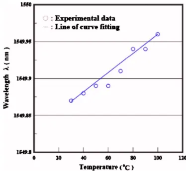
FIG. 1. 共Color online兲 Shift of center wavelength under different tempera-tures for NBPF with F7 substrate.
IV. RESULTS AND DISCUSSION
Five-cavity subnanometer bandwidth filter of the design, S / 3L共HL兲6 H 8L H 共LH兲6 L 关共HL兲7 H 8L H 共LH兲7L兴3H 共LH兲6 8L H共LH兲5L
⬘
H⬘
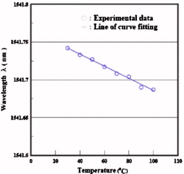
/air, is adopted in the analysis. The total number of film layers, therefore, is 187. The materials of high and low refractive indices are Nb2O5 and SiO2, re-spectively. The central wavelength shifts of NBPFs, indi-vidually deposited on F7 and WMS-02 substrates, under dif-ferent temperature rises are measured and plotted, as shown by the dots in Figs.1 and2, respectively. It is interesting to find that there exist different shifts for these two NBPFs deposited on different substrates. The NBPF of F7 presents a redshift, while the NBPF of WMS-02, on the contrary, re-veals a blueshift as the temperature increases. These experi-mental data can be approximately represented by the linear relations ⌬=0.0013⌬T+1549.8 and ⌬=−0.0008⌬T + 1541.8, respectively.The mechanical and optical properties of the thin films and substrates are given in Table I. It is worthy to mention that compared to the oxides of the other transition metals the phase diagram of Nb2O5 is rather complicated. So far the existence of at least 12 distinguishable phases has been
re-ported in the literature.15They are commonly divided into a few high- and low-temperature phases, and the transition be-tween them occurs in the range of 800– 1100 ° C. Moreover, it was found that the films deposited by midfrequency共MF兲 magnetron sputtering are most probably made up of nano-crystalline␦-Nb2O5, the first low-temperature phase. At nor-mal conditions ␦-Nb2O5 further transforms into the second low-temperature phase ␥-Nb2O5 upon heating around 570 ° C. It can be assumed that this phase transformation transformed into a denser form rather than a transition into a new lattice. Young’s moduli of␦-Nb2O5and␥-Nb2O5phases are approximately equal to 60 and 67.5 GPa, respectively.14 For amorphous Nb2O5 film, its Young’s modulus could be near to that of␦-Nb2O5.
The stress-optical coefficient, 共n /兲T, and
thermal-optical coefficient, 共n /T兲, for dielectric oxide film mate-rials, such as TiO2, Ta2O5, Nb2O5, and SiO2, have not been sufficiently clarified. According to the limited data available at hand, the magnitudes of 共n /兲T and 共n /T兲 for the
material SiO2 are equal to −3.53⫻10−12Pa−1 共Ref. 9兲 and 1.18⫻10−5° C−1,16,17 respectively. The corresponding data for Nb2O5film material, however, are still absent in the lit-erature and will be determined in this article.
The thermal stresses induced in the thin films due to temperature rise are evaluated by improved laminate model and shown in Table II, where the x axis is parallel to the plane of thin film layers.
In this study, only the stress-optical coefficient, 共n /兲T, and thermal-optical coefficient, 共n /T兲, of the
film material, Nb2O5, are unknown properties. These two properties can be easily evaluated inversely and are given in Table III. It has been reported14 that the value of ⌬n/⌬, similar to the definition of the stress-optical coefficient, for a number of Nb2O5film samples deposited by both dc and MF magnetron sputtering processes under various process pa-rameters is confined within the range from −100⫻10−12to − 800⫻10−12Pa−1. Since the index of refraction of a material is correlated to its density, it can be assumed that with an increased particle bombardment in the film deposition pro-cess the associated densification propro-cess will yield less level
FIG. 2. 共Color online兲 Shift of center wavelength under different tempera-tures for NBPF with WMS-02 substrate.
TABLE I. Material properties of film layers and substrate共Refs.10–14兲.
Young’s modulus 共GPa兲 Coefficient of thermal expansion 共ppm °C−1兲 Optical refractive index Poisson’s ratio Film Nb2O5 60 5.8 2.32 0.2 Film SiO2 74.5 0.55 1.46 0.164 Substrate WMS-02 85 10.1+ 0.015共T-20兲 20 ° C⬉T⬉100 °C 1.569 0.2 Substrate F7 55 9.8+ 0.006 43共T-20兲 20 ° C⬉T⬉100 °C 1.606 0.2
TABLE II. Thermal stressxxinduced in thin films due to temperature rise
⌬T=70 °C for two different NBPFs.
Substrate of NBPF
Thermal stressxx共MPa兲
Nb2O5 SiO2
WMS-02 22.7–22.9 60.9–61.2 F-7 19.2–19.5 57.0–57.2
TABLE III. The stress-optical and thermal-optical coefficients of film ma-terial Nb2O5. Film material Thermal-optical coefficient
共
n T兲
Stress-optical coefficient共
n 兲
T Nb2O5 1.43⫻10−5° C−1 −95.1⫻10−12Pa−1of porosity and higher values of the refraction index. More-over, it is obvious that for the same material a less level of porosity will correspond to a smaller value of the stress-optical coefficient. Compared to previous dual magnetron sputtering process, since a less level of porosity or denser film material can be achieved by IAD process, a smaller value of the stress-optical coefficient, −95.1⫻10−12Pa−1, might be a reasonable result.
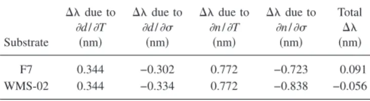
Moreover, contributions of four factors, i.e., the change of film thickness due to temperature rise 共⌬T=70 °C兲, d /T, and thermal stress,d /, as well as the change of refractive index due to temperature rise,n /T, and thermal stress, n /, on the shifts of central wavelength for two different NBPFs, with substrates F7 and WMS-02, respec-tively, are evaluated and given in TableIV. It is seen that for the same temperature rise the thermal stress induced in the thin films plays a key role on the final situation of central wavelength shift. The substrate WMS-02, in comparison with F7, has higher Young’s modulus and a larger difference in thermal expansion coefficient between substrate and film materials. Therefore, higher tensile thermal stress will be in-troduced in the thin films. Consequently, higher tensile ther-mal stress induces a more decrease in film thickness and refractive index, or the redshift of central wavelength in WMS-02 NBPF.
V. CONCLUDING REMARKS
In this article, two five-cavity thin film NBPFs are fab-ricated by using the same Nb2O5 and SiO2 film materials
individually deposited on different substrates, F7 and WMS-02, by IAD process. It is observed that the NBPF of F7 presents a redshift, while the NBPF of WMS-02, on the con-trary, reveals a blueshift as the temperature increases. The mechanism and theory related to this central wavelength shift due to temperature change are investigated and dis-cussed. It is found that the different levels of thermal stress induced in the thin films of two NBPFs play a key role on the final situation of central wavelength shift. Moreover, the magnitudes of the stress-optical and the thermal-optical co-efficients of Nb2O5thin film material are evaluated by mea-suring the data of central wavelength shifts due to a tempera-ture rise. These coefficients are evaluated and approximately equal to −95.1⫻10−12Pa−1 and 1.43⫻10−5° C−1, respec-tively.
ACKNOWLEDGMENT
The authors gratefully acknowledge the support of the National Science Council of Taiwan, R.O.C. 共Grant Nos. NSC 89-2215-E-006-001 and NSC 92-2212-E-006-020兲.
1H. Takashashi, Appl. Opt. 34, 667共1995兲.
2S. Sakaguchi, Jpn. J. Appl. Phys., Part 1 38, 6362共1999兲.
3T. C. Chen, J. I. Kuo, W. L. Lee, and C. C. Lee, Jpn. J. Appl. Phys., Part
1 40, 4087共2001兲.
4J. C. Hsu, C. C. Lee, C. C. Kuo, S. H. Chen, J. Y. Wu, H. L. Chen, and C.
Y. Wei, Appl. Opt. 44, 4402共2005兲.
5T. C. Chen, H. C. Wu, and C. L. Lin, J. Cryst. Growth 249, 44共2003兲. 6H. A. Macleod, Thin-Film Optical Filters, 2nd ed.共McGraw-Hill, New
York, 1989兲.
7A. Zoller, R. Gotzelmann, K. Malt, and D. Cushing, Appl. Opt. 35, 5609
共1996兲.
8J. F. Nye, Physical Properties of Crystals: Their Representation by
Ten-sors and Matrices共Oxford Science, New York, 1992兲.
9W. Lukosz and P. Pliska, Opt. Commun. 117, 1共1995兲. 10W. Primak and D. Post, J. Appl. Phys. 30, 779共1959兲. 11S. Spinner, J. Opt. Soc. Am. 45, 394共1962兲. 12Optical Silica共Electro-Quartz, New York, 1987兲, p. 4.
13G. L. Dwivedi and E. C. Subbaro, J. Am. Ceram. Soc. 56, 443共1973兲. 14H. Hunsche, M. Vergöhl, H. Neuhäuser, F. Klose, B. Szyszka, and T.
Matthée, Thin Solid Films 392, 184共2001兲.
15E. I. Ko and J. G. Weissmann, Catal. Today 8, 27共1990兲. 16I. H. Malitson, J. Opt. Soc. Am. 55, 1205共1965兲.
17J. Jasny, B. Nickel, and P. Borowicz, J. Opt. Soc. Am. B 21, 729共2004兲.
TABLE IV. Contributions of the change of refractive index and film thick-ness due to temperature rise共⌬T=70 °C兲 and thermal stress on shift of center wavelength. Substrate ⌬ due to d /T 共nm兲 ⌬ due to d / 共nm兲 ⌬ due to n /T 共nm兲 ⌬ due to n / 共nm兲 Total ⌬ 共nm兲 F7 0.344 −0.302 0.772 −0.723 0.091 WMS-02 0.344 −0.334 0.772 −0.838 −0.056