Modifications of Low Dielectric Constant Fluorinated Amorphous Carbon Films by Multiple Plasma Treatments
Jia-Min Shieh,a,zKou-Chiang Tsai,aBau-Tong Dai,a Shih-Chin Lee,bChih-Hung Ying,band Yan-Kun Fangc
aNational Nano Device Laboratories, Hsinchu 30050, Taiwan
bDepartment of Materials Science and Engineering,cDepartment of Electrical Engineering, National Cheng-Kung University, Taiwan
This study investigated the material and electrical characteristics of hydrogen, nitrogen plasma-treated fluorinated amorphous carbon共a-C:F兲 films in relation to their thermal stability. Experimental results indicate that the nitridation passivation layer and hydrogen passivated chemical bonds on the film surface effectively suppress thermal decomposition during high temperature annealing. Accordingly, a multiple plasma treatment on a-C:F films was proposed. In this treatment, nitrogen plasma nitridation was performed not only to passivate the a-C:F films against copper diffusion, but also to prevent the fluorine contents from penetrating into copper intermetals. Hydrogen plasma treatment then recovered unstable bonds formed during the nitridation process, thus yielding stable chemical structures and inducing hydrophobic characteristics of the film surface. The multiple plasma-treated a-C:F films demonstrated the desired performance as interlayer dielectrics.
© 2002 The Electrochemical Society. 关DOI: 10.1149/1.1481069兴 All rights reserved.
Manuscript submitted August 17, 2001; revised manuscript received January 24, 2002. Available electronically May 14, 2002.
Low dielectric constant共low-k兲 materials as interlayer dielectrics 共ILDs兲, deposited either by chemical vapor deposition 共CVD兲 or spin-on techniques,1encounter similar difficulties, such as integra- tion issues,2weak resistance to copper diffusion,3and the require- ment of blocking corrosion species that would otherwise penetrate into intermetals.4 Low-k materials such as black-diamond Si-C films5and fluorinated amorphous carbon共a-C:F兲 films6are attract- ing increasing interest since they can be deposited by conventional plasma-enhanced chemical vapor deposition 共PECVD兲 methods.
The gaseous mixture containing fluorocarbon and hydrocarbon is a precursor for depositing a-C:F films,6 making the deposition of a-C:F films as easy as preparing fluorinated SiO2共SiOF兲 films.
Several attempts have been made to address and improve critical areas regarding material properties of a-C:F films in the interconnect processes.6-12Yang et al. elucidated the structural evolution of the a-C:F film during thermal annealing.7Yokomichi further indicated that the dangling bond density increased after annealing a-C:F films at 400°C.9 Optimizing the processing parameters enables a-C:F films with better characteristics to be deposited as an ILD.10How- ever, the electrical characteristics of a-C:F films become degraded even after annealing at several hundred degrees, typically about 400°C,11as most of the low-k materials. This intrinsic, fatal problem seriously limits their application as ILDs.
Previous studies have demonstrated that plasma post-treatment is an effective means of modifying as-deposited dielectric films.13-17 Hydrogen plasma treatment can typically recover unstable bonds, or defect sites, into stronger chemical structures.14-16The treated films exhibited better resistance to moisture uptake and even copper dif- fusion, and unaffected electrical characteristics when annealed.15,16 On the other hand, the NH3-plasma nitridation on interlayer films can block the penetration for copper into ILD, and hinder the hy- groscopic behaviors of low-k films.17However, relevant integration issues for fluorinated dielectrics, such as a-C:F, SiOF, include the degassing of fluorine into nearby metals, or dielectric layers, causing metal corrosion or etching of the dielectrics.4,13,18The extent of the precipitation of fluorine in the a-C:F film greatly exceeds that of SiOF, requiring additional shielding.
This work demonstrates the feasibility of applying multiple plasma treatment to a-C:F films. Nitrogen plasma nitridation is per- formed not only to passivate the a-C:F films against copper diffu- sion, but also to block the erosive fluorine contents from penetrating into copper intermetals via the nitridation passivation layer. Hydro-
gen plasma treatment then recovers unstable bonds formed during the nitridation process, thus yielding stable chemical structures. The postdeposition parameters can be separately optimized since mul- tiple plasma treatment is performed. The proposed approach can recover the electrical degradation caused by nitrogen plasma post- deposition and prevent a large amount of hydrogen, as decomposed from NH3 plasma, from bonding with fluorine species, and then degassing via the HF structure. Combining the postdeposition of N2
and H2yields a better performance over that of conventional single plasma, or mixed plasma treatments.
Experimental
As-deposited a-C:F films were deposited by PECVD. The basic precursor gas was a mixture of CH4, and CxFy 共CF4, C2F6, or C4F8兲. As in our previous work,10the optimum deposition param- eters for a-C:F films were CxFy/CH4~10, radio frequency 共rf兲 plasma power 200 W, process pressure 550 mTorr, and deposition temperature 250°C. The total gas flow used for depositing the a-C:F films was 300 standard cubic centimeters per minute共sccm兲. In this experiment, another class of samples was the NH3, N2, and H2 plasma-treated a-C:F films. For simplicity, STD represents the as- deposited a-C:F films, whereas N-3, N-6, and N-9 represent as- deposited a-C:F films with N2plasma treatments of 3, 6, and 9 min, respectively. Additionally, H-3, H-6, and H-9 represented as- deposited a-C:F films with H2plasma treatment for 3, 6, and 9 min, respectively. The postdeposition parameters of NH3, N2, and H2
plasma treatments were rf plasma power 200 W, process pressure 100 mTorr, substrate temperature 250°C, and flow rate 200 sccm.
Table I lists the deposition and postdeposition parameters. Thermal stability was then examined by curing those a-C:F films in a furnace at elevated temperatures for 30 min in N2ambient at a flow rate of 10 L/min. The thicknesses and refractive indices of those films were determined by a n and k analyzer. Before and after each treatment, the Fourier transform infrared共FTIR兲 absorption spectra and X-ray photoelectron spectroscopy 共XPS兲 of each film were examined to monitor structural changes. Secondary ion mass spectroscopy 共SIMS兲 was carried out to analyze not only the degrees of copper diffusion in the a-C:F films, but also the outgassing of fluorine con- tents into the intermetals. Thermal desorption spectroscopy 共TDS兲 determined the extent of desorption of various bonding classes共such as H2O兲 in the a-C:F films, to compare the effects of the postdepo- sition parameters on thermal stability and the resistance to moisture.
Finally, electrical measurements were taken by using metal- insulator-semiconductor共MIS兲 capacitors.
zE-mail: jmshieh@ndl.gov.tw
Results and Discussion
Fundamental characteristics of plasma modified low-K a-C:F films.—Tables IIa and b list the basic characteristics for as-deposited a-C:F films, indicating that the best performing a-C:F films are de- posited by a mixture of CH4and C4F8. The dielectric constant is as low as 2.35, and the leakage current can be maintained below Id⬇ 6.0 ⫻ 10⫺9A/cm2 at a bias electric field of Ebias
⫽ 1.0 MV/cm. All a-C:F films discussed in this study were depos- ited by a mixture of CH4and C4F8. After annealing at 450°C, the dielectric constant and leakage current markedly increased to 3.68 and Id⬇ 5.0 ⫻ 10⫺7 A/cm2respectively, although the film shrink- age was below 2.5%. Closely examining XPS spectra in Table IIb reveals that the calculated fluorine/carbon 共F/C兲 ratio8 also de- creased from 0.98 to 0.83. Therefore, an additional modification such as plasma treatments on as-deposited a-C:F films was required in addition to the optimization of deposition conditions.
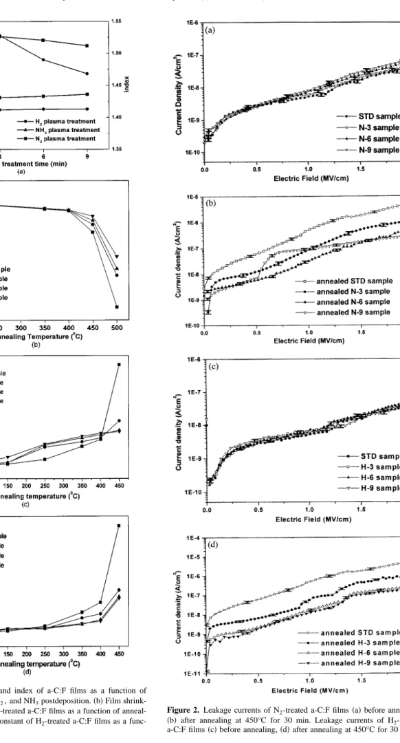
Figure 1a illustrates the film shrinkage of a-C:F films after NH3, N2, and H2plasma treatments at various process times共films’ thick- ness,⬃5000 Å兲. The NH3 plasma treatment is not applicable to a-C:F films since its refractive index, thickness changed by more than 9% in the 1.5 min process time, although NH3 plasma effec- tively modified many materials.17Therefore, nitrogen and hydrogen plasma treatments were adopted herein. Figure 1b indicates that the N2 plasma-treated a-C:F films can maintain their thickness after 450°C annealing 共1% thickness loss in the best case兲. Figure 1c displays the dielectric constants of N2-treated a-C:F films as a func- tion of annealing temperature. Although the dielectric constants of N2-treated a-C:F films did not change, Fig. 2a indicates that the leakage currents of N2-treated samples slightly increased. We can infer that this phenomenon is owing to the formation of a few un- stable bonds on the film surface during nitrogen plasma treatment.
Nevertheless, the dielectric constants of the bulk films of the as- treated samples remained unaffected. Thus, FTIR spectra for the chemical structures of those samples are the same as those of the as-deposited samples, as shown in Fig. 3a.
Figures 1d and 2c summarize the corresponding measurements for H2-treated samples. In contrast to N2-treated a-C:F films, both
the dielectric constants and leakage currents of a-C:F films treated by H2plasma remain unchanged. The hydrogen plasma can deeply penetrate into a-C:F films and recover the unstable bonds or defect sites, into stable chemical bonds. Consequently, the leakage currents and dielectric constants of H2-treated films can be improved or at least maintained. FTIR spectra for the chemical structures of such films are the same as those of the as-deposited samples, as shown in Fig. 3c.
Notably, a-C:F films are also characterized by the slight increase of their compressive stresses from⫺10 to ⫺12 Mpa after N2 and N2/H2 postdepositions because of the formation of more dense films by postdeposition treatment. Also, stresses of the H2-treated Table I. Deposition and postdeposition parameters.
Deposition parameter Postdeposition parameter Reactant gases CxFy/CH4⬃10 NH3, N2, and H2
RF plasma power 200 W 200 W
Process pressure 550 mTorr 100 mTorr
Temperature 250°C 250°C
Flow rate 300 sccm 200 sccm
Table II.a. Fundamental characteristics for a-C:F films. Changes in dielectric constants, leakage currents, and X-ray photoelectron spectros- copy of a-C:F films, after thermal annealing at 450°C for 30 min are shown for comparison.
Mixture gases CF4with CH4 C2F6with CH4 C4F8with CH4
Deposition rate 190 Å/min 1000 Å/min 550 Å/min
Stress ⫺45 Mpa ⫺25 Mpa ⫺10 Mpa 共no treatment兲
⫺10 Mpa 共H2treatment兲
⫺12 Mpa 共N2treatment兲
⫺12 Mpa 共N2/H2treatment兲 Dielectric constant
共Al gates兲 2.85-4.5 2.6-3.9 2.35-3.68
Leakage current
共Al gates兲 6.0⫻ 10⫺8to 2.0⫻ 10⫺6A/cm2 2.0⫻ 10⫺8to 6.0⫻ 10⫺7A/cm2 6.0⫻ 10⫺9to 5.0⫻ 10⫺7A/cm2 Shrinkage
(⌬d/d) at 450°C ⬎0.15 ⬍0.05 ⬍0.03
F/C ratio 共calculated from XPS spectra兲
0.47-0.36 0.84-0.81 0.98-0.83
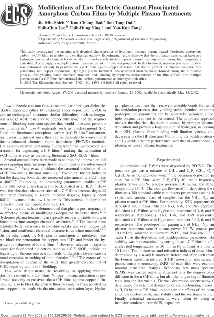
Table II.b.
Figure 1. 共a兲 Film shrinkage, and index of a-C:F films as a function of plasma treatment time for N2, H2, and NH3postdeposition.共b兲 Film shrink- age共c兲 Dielectric constant of N2-treated a-C:F films as a function of anneal- ing temperature.共d兲 Dielectric constant of H2-treated a-C:F films as a func- tion of annealing temperature.
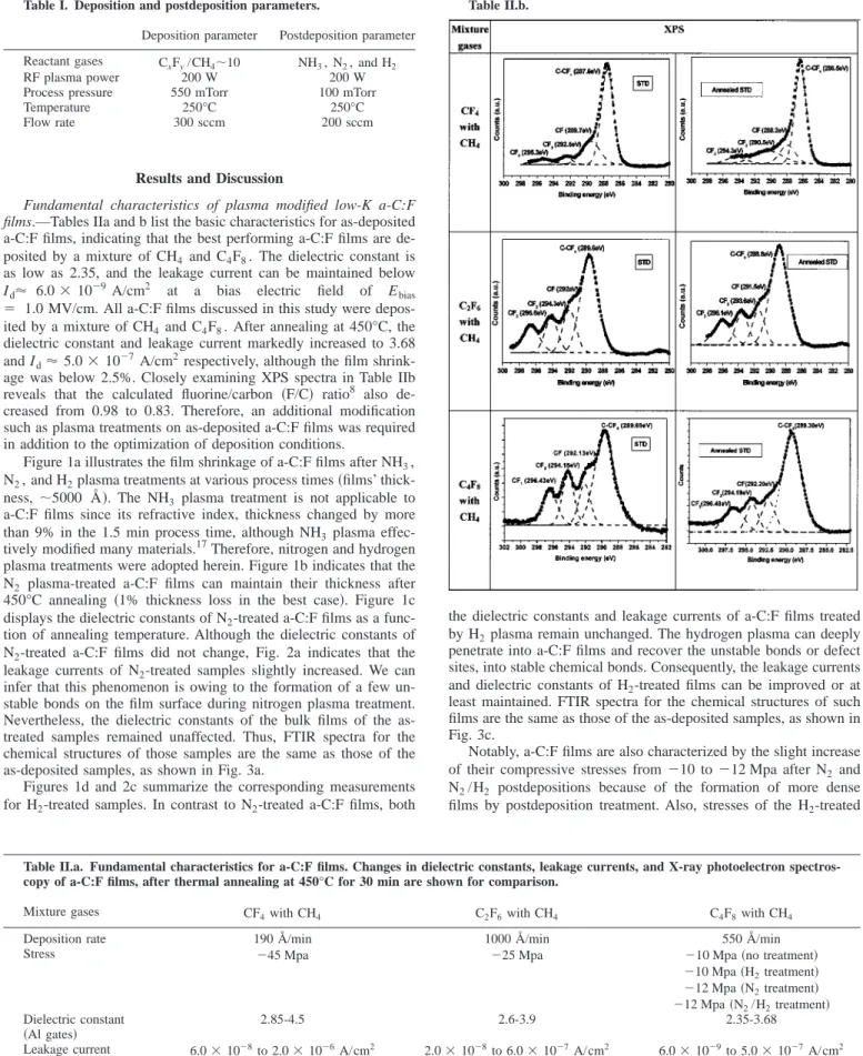
Figure 2. Leakage currents of N2-treated a-C:F films共a兲 before annealing, 共b兲 after annealing at 450°C for 30 min. Leakage currents of H2-treated a-C:F films共c兲 before annealing, 共d兲 after annealing at 450°C for 30 min.
a-C:F films are maintained at the same level as those of untreated films because the hydrogen gases have less of a densification effect on a-C:F films than nitrogen gases do. This nitrogen plasma bom- bardment introduces either steric strains or nonoptimum bond angles in the a-C:F films, resulting in fewer unstable bonds in the N2-treated a-C:F films. Damage incurred from the nitrogen plasma is more serious than that from the hydrogen plasma owing to the heavier nitrogen atoms and radicals of the former. In addition, some dangling bonds caused by deposition, postdeposition processes or thermal stresses may temporarily exist on the film surface. Those unstable sites tend to react with other species共i.e., moisture兲 from the environment, thus degrading the electrical characteristics共a for- mation of CvO兲. However, the effect of imperfect bonds on de- grading electrical characteristics can be decreased by either an inert passivation layer on the film surface共nitridation process兲 or forma- tion of stable bonding structures共hydrogen passivated bonds兲.
Thermal stabilities of modified low-k a-C:F films.—Figures 1c and d for the N2- and H2-treated a-C:F films reveal that the dielec- tric constant increases from 2.35 to 2.8 as the annealing temperature increases to 450°C. In comparison, the untreated sample abruptly changes its electrical characteristics, and its dielectric constant rises to 3.7 such that the thermal stability of the dielectric constants of a-C:F films is significantly improved after treatment with H2or N2
plasma. Some interesting observations can be made about improve- ments of those two processes. First, at lower annealing temperatures Figure 3. FTIR spectra of N2-treated a-C:F films共a兲 before annealing, 共b兲
after annealing at 450°C for 30 min. FTIR spectra of H2-treated a-C:F films 共c兲 before annealing, 共d兲 after annealing at 450°C for 30 min.
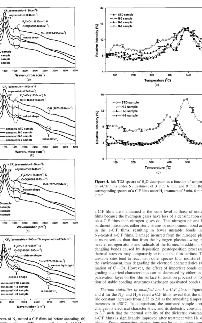
Figure 4. 共a兲: TDS spectra of H2O desorption as a function of temperature of a-C:F films under N2 treatment of 3 min, 6 min, and 9 min.共b兲 The corresponding spectra of a-C:F films under H2treatment of 3 min, 6 min, and 9 min.
(⬍400°C), the resistance of as-deposited films to thermal stresses is better than that of N2-treated samples. In contrast, the H2-treated samples exhibited better thermal stability than that of untreated samples. Second, the modifications of a-C:F films by both of these postdeposition processes saturate at specified times, at which the N-6, H-6 samples behave like N-9 and H-9 samples, respectively.
Finally, the H2-treated samples exhibit a higher resistance to thermal stresses than the N2-treated samples do, as observed from Fig. 1c, d and 2b, d.
As mentioned earlier, unstable bonds in N2-treated samples ap- peared. By increasing the hydrophilic nature of the film surface, these bonds facilitate the uptake of moisture and increase the dielec- tric constants of the samples, especially under thermal stresses. In addition to confirming the more hydrophilic nature of the surfaces of the N2-treated samples, TDS spectra in Fig. 4a also verified that the desorption abundanceof H2O of the N-9 sample was higher than for any other sample. Therefore, the N2-treated samples exhibited a worse thermal stability than did the as-deposited samples at lower annealing temperatures (⬍400°C), as shown in Fig. 1c. However, the dielectric constants of N2-treated a-C:F films increased only from 2.35 to 2.8 as the annealing temperature rose to 450°C. In comparison, the dielectric constant of the untreated sample abruptly increased to 3.7. These results correspond to those in Fig. 2b, which shows that the leakage currents of the N-6 and N-9 samples were also markedly lower than those of the N-3 and STD samples at this higher annealing temperature of 450°C. The leakage current of the N-6 sample only increased from Id⬇ 6.0 ⫻ 10⫺9 A/cm2 to Id
⬇ 3.8 ⫻ 10⫺8A/cm2 共at Ebias⫽ 1.0 MV/cm兲 after thermal an- nealing at 450°C. In comparison, the leakage currents of N-3 and STD samples increased to Id⬇ 1.0 ⫻ 10⫺7 and Id⬇ 5.0
⫻ 10⫺7 A/cm2, respectively. These results suggest that N2-treated a-C:F films are involved in mechanisms other than the creation of a few unstable bonds by nitrogen plasmas.
In fact, the N2-plasma treatment on a-C:F films simultaneously forms fewer unstable bonds and nitridation layers on the film sur- face. SIMS measurements and investigations of copper diffusion verify the formation of a nitridation passivation layer. This passiva- tion layer on the film surface effectively suppresses the degradation due to accompanying unstable bonds. Therefore, at low temperature annealing, the defects of the N2-treated samples cause a worse per- formance of the electrical characteristics than those of untreated ones. In contrast, for annealing temperatures exceeding 400°C, the highly nitrated samples共N-6, N-9兲 exhibited better electrical char- acteristics than did the lightly treated sample共N-3兲, or the untreated sample since the chemical structures of weakly passivated samples 共N-3, STD兲 seriously decomposed at higher thermal stresses.
Figure 3b indicates that the major FTIR spectral peaks of CFx (980-1350 cm⫺1) and C-H (2873-2954 cm⫺1)12 of the annealed N-6 and N-9 samples are similar to those of the STD samples.
However, few defect sites due to damage of annealed N-6 and N-9 samples from nitrogen plasma still induce slightly hydrophilic char- acteristics in the film surface when the higher temperature stresses are applied to those films. Hence, a peak shape was observed for CvO bonds 共1650 and 1850 cm⫺1兲 in the FTIR spectra, as com- pared to the obtuse shape observed for the STD samples in Fig. 3a.
On the other hand, weakly passivated N-3 STD samples begin to decompose their chemical bonds, some of which are reconstructed at higher annealing temperatures共above 400°C兲. The appearance of a small bulge located at the CuH bond confirms thermal decompo- sition of annealed STD and N-3 samples, because the ratio of CFx bonds in a-C:F films decreased and the related dielectric constants increased after annealing at 450°C. The F/C ratio in Table IIb con- firm the reduction of the ratio of CFxbonds in a-C:F films. In fact, a higher C-H peak in the FTIR spectrum was also detected for the a-C:F films deposited at lower CxFy/CH4 ratios 共data not shown here兲. Finally, the N-6 sample exhibited thermal stabilities better than the N-9 sample as their dielectric constants共Fig. 1c兲, leakage
currents共Fig. 2b兲, and TDS spectra 共Fig. 4a兲 are compared. In sum, the nitridation passivation competes with the degradation from ac- companying unstable bonds. This effect is believed to be a major mechanism.
The unstable bonds of the untreated samples are few, and can thus resist thermal stress up to 250°C, as shown in Fig. 1d. Above that temperature, the decomposition of CuFx bonds in untreated a-C:F films begins. H2-treated samples are almost unaffected at such low temperatures. Furthermore, strongly H2-passivated samples 共H-6, H-9兲 were more stable than other samples at all annealing temperatures. After thermal annealing at 450°C for 30 min, the leak- age currents of H-6 and H-9 samples were also much lower than those of H-3 and STD samples, as depicted in Fig. 2d. Therefore, hydrogen plasma treatment plays a role of stabilizing chemical structures of a-C:F films. This effect is due to a formation of hydro- gen passivated chemical structures in the films and this modified characteristic for H2-treated a-C:F films can suppress the uptake of moisture and reduce thermal decomposition during high temperature annealing. TDS spectra in Fig. 4b verified the presence of more hydrophobic surfaces in the H2-treated samples than in the others, and that the desorption abundance of H2O of the H-9 sample is the least among all samples. Figure 3d also reveals that spectral peaks of CFx(980-1350 cm⫺1) and C-H (2873-2954 cm⫺1)12and the obtuse shape of the CvO bond in the FTIR spectrum of the annealed H-6 and H-9 samples appear as those of the STD sample. In comparison, significant peaks at the CvO and CuH bonds appeared for an- nealed H-3 and STD samples since reconstruction 共CuH bonds兲 and the moisture uptakes 共CvO bonds兲 occurred in the weakly passivated films. Furthermore, the leakage current of H-6 and H-9 samples only increased from Id⬇ 6.0 ⫻ 10⫺9 A/cm2to Id⬇ 1.28
⫻ 10⫺8 A/cm2 共at Ebias⫽ 1.0 MV/cm兲 after thermal annealing at 450°C. The values for annealed H-3 and STD samples are Id
⬇ 5.8 ⫻ 10⫺8and Id⬇ 5.0 ⫻ 10⫺7A/cm2, respectively.
However, Fig. 1d, 2d, 3d, and 4b reveal that the thermal stability of the H-9 sample behaved like that of the H-6 sample. An excess of hydrogen atoms in the H-9 sample, which might break the CFx bonds and actively react with fluorine species before outgassing via HF structures at elevated thermal stresses, was believed to be the major reason for the saturation of treatment times. As a result, a small C-H signal for the annealed H-9 sample actually existed, re- vealing reconstruction in highly H2-treated samples after annealing.
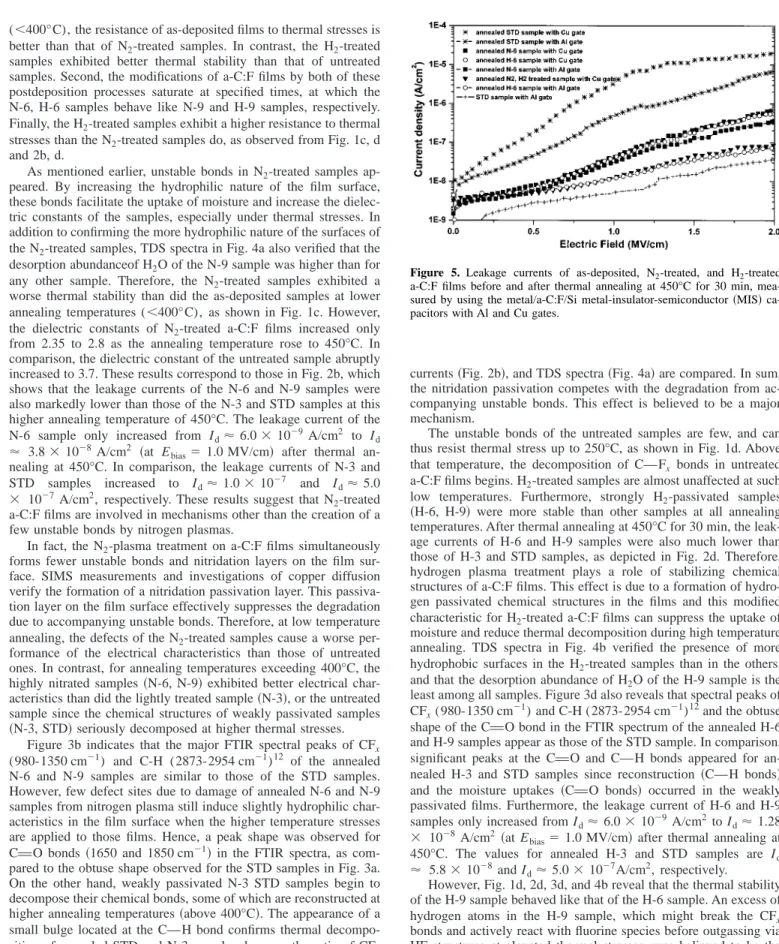
Considering the dielectric constants and leakage currents to- gether, the H2 treatment time of 6 min is enough to inhibit the degradation caused by thermal stresses and achieve better thermal stabilities than the N2-treated samples. However, N2-plasma nitrida- Figure 5. Leakage currents of as-deposited, N2-treated, and H2-treated a-C:F films before and after thermal annealing at 450°C for 30 min, mea- sured by using the metal/a-C:F/Si metal-insulator-semiconductor共MIS兲 ca- pacitors with Al and Cu gates.
tion might provide a barrier to copper diffusion and fluorine out-gassing.
Inhibition of copper diffusion and outgassing of corrosive fluorine species.—The last section addresses the material and elec- trical properties of plasma-treated a-C:F films with regard to thermal stabilities, and the optimal postdeposition conditions are obtained.
As discussed, both the nitridation passivation layer and hydrogen- passivated bonding structures on surfaces of treated a-C:F films ef- fectively suppress thermal decomposition during high temperature annealing. However, low-k materials are normally employed as in- terlayers in copper damascene interconnects. Thus, the barrier effect of treated a-C:F films against copper diffusion must be discussed.
Figure 5 shows the leakage currents of annealed N-6 and H-6 samples with Cu and Al electrodes in MIS capacitors. The annealing temperature and process time were 450°C and 30 min, respectively.
The behavior of the leakage current of samples with Cu penetration was well explained by the Poole-Frenkel 共P-F兲 mechanism.17,19 Best-fitting yielded the slopes of the leakage curves in the cases considered here:PF is in the range 5.8⫻ 10⫺24 to 6.6⫻ 10⫺24; the P-F mechanism dominates the transportation of carriers through Cu/a-C:F/Si capacitors.17 Furthermore, the leakage current of the annealed H-6 sample with the Cu gate obviously increases to Id
⬇ 4.5 ⫻ 10⫺8A/cm2 共at Ebias⫽ 1.0 MV/cm兲, as compared with
Id⬇ 1.2810⫺8A/cm2for the Al gate. For the annealed N-6 sample, the change in leakage curves is significantly smaller than that for the H-6 sample, and the relevant values are Id⬇ 5.0 ⫻ 10⫺8 A/cm2 and Id⬇ 3.8 ⫻ 10⫺8A/cm2for the Cu and Al gates, respectively.
For the samples without postdeposition, the leakage current abruptly increases by one order of magnitude higher than that of treated samples. In conclusion, the nitridated surface of a-C:F film effi- ciently blocks copper diffusion and protects a- C:F films from ther- mal decomposition.
Figure 6a presents the SIMS analysis of the bare N-6 sample.
From this figure, a distribution profile of nitrogen elements near the a-C:F surface was determined. The penetration depth of about 25 nm resembles that given in other studies.17In contrast, no obvious ni- trogen elements were found inthe H-6 sample, as shown in Fig. 6b.
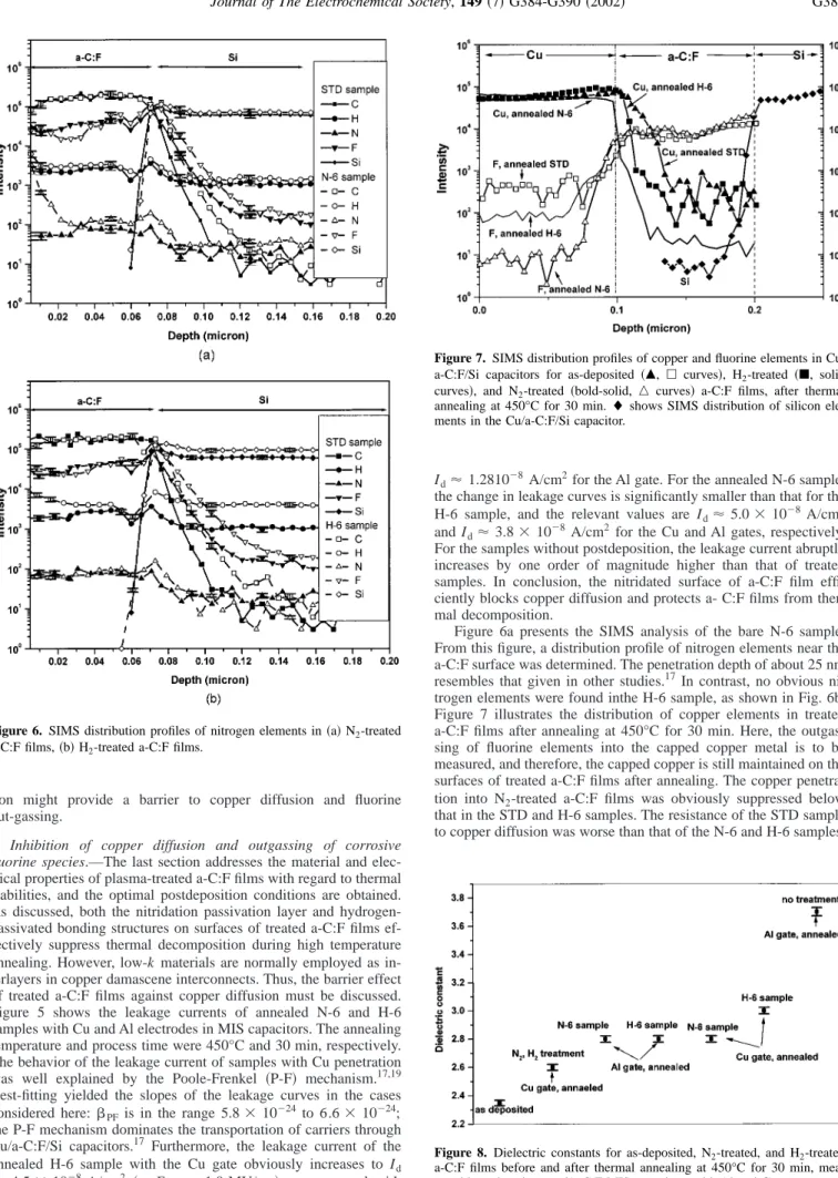
Figure 7 illustrates the distribution of copper elements in treated a-C:F films after annealing at 450°C for 30 min. Here, the outgas- sing of fluorine elements into the capped copper metal is to be measured, and therefore, the capped copper is still maintained on the surfaces of treated a-C:F films after annealing. The copper penetra- tion into N2-treated a-C:F films was obviously suppressed below that in the STD and H-6 samples. The resistance of the STD sample to copper diffusion was worse than that of the N-6 and H-6 samples.
Figure 6. SIMS distribution profiles of nitrogen elements in共a兲 N2-treated a-C:F films,共b兲 H2-treated a-C:F films.
Figure 7. SIMS distribution profiles of copper and fluorine elements in Cu/
a-C:F/Si capacitors for as-deposited共䉱, 䊐 curves兲, H2-treated共䊏, solid curves兲, and N2-treated共bold-solid, 䉭 curves兲 a-C:F films, after thermal annealing at 450°C for 30 min.⽧ shows SIMS distribution of silicon ele- ments in the Cu/a-C:F/Si capacitor.
Figure 8. Dielectric constants for as-deposited, N2-treated, and H2-treated a-C:F films before and after thermal annealing at 450°C for 30 min, mea- sured by using the metal/a-C:F MIS capacitors with Al and Cu gates.
This finding corresponds to the nitrogen distributions in those samples, as shown in Fig. 6, and explains the changes in measured leakage currents for N2 and H2-treated samples with Al and Cu gates, as shown in Fig. 5.
Another contribution for nitrogen plasma treatments is the inhi- bition of fluorine contents outgassing into capped copper metals, as depicted in Fig. 7. According to this figure, the intensity of fluorine contents in the N-6 sample is smaller than that in the H-6 sample, while the untreated sample is the worst. The fluorine contents are generally present in the fluorocarbon species (CFx), since these spe- cies are the major chemical constituents of a-C:F films and are often observed in TDS spectra, where F, HF is difficult to detect due to the reaction of those gases with Si/SiO2 in the measurement system, leading to the formation of SiF4.12On the other hand, charged HF species are required by the TDS approach and only a few of them are formed. In general, a portion of the fluorocarbon species in the a-C:F films, as a terminal group, might react with environmental moisture and form corrosive HF which corrodes metals. The stabil- ity of the chemical bonds in the H-6 sample cause fewer fluorine species to be desorbed than those from the N2-treated sample. How- ever, the electrical characteristics of N2-treated and H2-treated samples after annealing are similar, likely owing to prevention of the outgassing of fluorine species by the nitridation layer of the N2-treated samples. Although nitridation accompanies bond damage, hydrogen-plasma treatment can recover unstable bonds, and a mul- tiple plasma treatment of a-C:F films is proposed. In this multiple plasma treatment the nitrogen plasma nitridation is performed not only to passivate the a-C:F films against copper diffusion, but also to prevent the erosive fluorine contents from penetrating into copper intermetals. Hydrogen plasma treatment then recovers unstable bonds formed during the nitridation process, thus yielding stable chemical structures. By adopting this novel approach, the leakage current for the multiple plasma-treated samples after annealing de- clines to Id⬇ 1.5 ⫻ 10⫺8 A/cm2for Cu gates, as shown in Fig. 5.
Figure 8 shows the dielectric constants of samples after those dif- ferent processes. The dielectric constant can be as low as 2.6 for the multiple plasma-treated a-C:F film in the Cu/a-C:F/Si capacitor after annealing at 450°C.
Conclusion
This study investigated the thermal stabilities of hydrogen and nitrogen plasma-treated fluorinated amorphous carbon films共a-C:F兲.
The a-C:F films modified by multiple plasma treatments demon- strate the desired characteristics as interlayer dielectrics, including high resistance to pyrolysis, copper diffusion, and penetration of
corrosive species into intermetals. The nitrogen plasma nitridation passivates the a-C:F films against copper diffusion. This nitridation passivation layer also prevents the corrosive species of low-k a-C:F films, for example F, from diffusing into copper intermetals. In do- ing so, additional hydrogen plasma treatment recovers the imperfect bonds formed during the nitridation process, yielding stable chemi- cal structures. Combining postdeposition of N2 with H2 offers re- markable improvements over conventional single plasma, or mixed plasma treatments. This novel approach can be applied to fluorinated dielectrics such as SiOF and a-C:F.
Acknowledgments
The authors thank the National Science Council of the Republic of China, Taiwan, for financial support of this research under con- tract no. NSC90-2721-2317-200.
The National Nano Device Laboratories assisted in meeting the publica- tion costs of this article.
References
1. L. Peter, Semicond. Int., 1998, 64共Sept兲.
2. M. Hiroi, M. Tada, H. Ohtake, S. Saito, T. Onodera, N. Furutake, Y. Harada, and Y.
Hayashi, in Proceedings of the 2001 International Interconnect Technology Con- ference, IEEE Electron Devices Society, p. 295共2001兲.
3. A. L. S. Loke, J. T. Wetzel, P. H. Townsend, T. Tanabe, R. N. Vrtis, M. P. Zussman, D. Kumar, C. Ryu, and S. S. Wong, IEEE Trans. Electron Devices, 46, 2178 共1999兲.
4. F. Iacona, G. Ceriola, and G. Spoto, J. Electrochem. Soc., 148, F47共2001兲.
5. B. K. Hwang, M. J. Loboda, G. A. Cerny, R. F. Schneider, J. A. Seifferly, and T.
Washer, in Proceedings of the 2000 International Interconnect Technology Confer- ence, IEEE Electron Devices Society, p. 52共2000兲.
6. K. Endo and T. Tatsumi, Appl. Phys. Lett., 68, 2864共1996兲.
7. H. Yang, D. J. Tweet, Y. Ma, and T. Nguyen, Appl. Phys. Lett., 73, 1514共1998兲.
8. Y. Ma, H. Yang, J. Guo, C. Sathe, A. Agui, and J. Nordgren, Appl. Phys. Lett., 72, 3353共1998兲.
9. H. Y. Komichi and A. Masuda, J. Appl. Phys., 86, 2468共1999兲.
10. J.-M. Shieh, S.-C. Suen, K.-C. Tsai, B.-T. Dai, Y.-C. Wu, and Y.-H. Wu, J. Vac. Sci.
Technol. B, 19, 780共2001兲.
11. S.-S. Han and B.-S. Bae, J. Electrochem. Soc., 148, F67共2001兲.
12. I. Banerjee, M. Harker, L. Wong, P. A. Coon, and K. K. Gleason, J. Electrochem.
Soc., 146, 2219共1999兲.
13. M. Du, R. L. Opila, V. M. Donnelly, J. Sapjeta, and T. Boone, J. Appl. Phys., 85, 1496共1999兲.
14. I. Wu, T. Huang, W. B. Jackson, A. G. Lewis, and A. Chiang, IEEE Electron Device Lett., 12, 181共1991兲.
15. Y. C. Quan, S. Yeo, C. Shim, J. Yang, and D. Jung, J. Appl. Phys., 89, 1402共2001兲.
16. T.-C. Chang, P.-T. Liu, Y.-J. Mei, Y.-S. Mor, T.-H. Perng, Y.-L. Yang, and S. M.
Sze, J. Vac. Sci. Technol. B, 17, 2325共1999兲.
17. P.-T. Liu, T.-C. Chang, Y.-L. Yang, Y.-F. Cheng, and S.-M. Sze, IEEE Trans. Elec- tron Devices, 47, 1733共2000兲.
18. K.-W. Lee, S. Lee, and J.-W. Park, J. Electrochem. Soc., 148, C131共2001兲.
19. S. M. Sze, Physics of Semiconductor Devices, Wiley, New York共1981兲.