行政院國家科學委員會專題研究計畫 成果報告
新穎材料開發關鍵核心設施計畫--磊晶氮氧物材料成長的
關鍵核心設施建置
研究成果報告(精簡版)
計 畫 類 別 : 整合型 計 畫 編 號 : NSC 98-2119-M-006-006- 執 行 期 間 : 98 年 06 月 01 日至 100 年 12 月 31 日 執 行 單 位 : 國立成功大學物理學系(所) 計 畫 主 持 人 : 黃榮俊 共 同 主 持 人 : 陳宜君、陳引幹、齊孝定、劉全璞、許進恭 計畫參與人員: 碩士班研究生-兼任助理人員:陳金宏 碩士班研究生-兼任助理人員:郭士銘 博士班研究生-兼任助理人員:黃舜漁 博士班研究生-兼任助理人員:董奕 博士班研究生-兼任助理人員:邱詩航 博士班研究生-兼任助理人員:蘇書玄 博士後研究:江岳峯 公 開 資 訊 : 本計畫可公開查詢中 華 民 國 101 年 05 月 31 日
中 文 摘 要 : 我們在國科會(新穎材料計劃)和成大配合款支助下,已在 2011 年 3 月初步完成南部磊晶平台雛型架構的建置,計有兩 台 PLD,一台 MBE (III-Nitride),一台 UHV Sputter,並已 完成三套磊晶系統(III- Nitride + PLD(2) + UHV
Sputter)的超高真空連結。目前 PLD(1)以成長簡單金屬氧化 物(ZnO, Fe3O4, MgO, ITO 等)已結合 III-Nitride LED 研 究—包括磊晶 ITO/doped ZnO 結合 III-N LED 以提升其發光 效率和 Spin-LED 研究等。PLD(2)以複雜化合物之測試成長為 主—初步包括磊晶 CIGS solar cell 多層膜和 Co:PbPdO2 零能隙半導體(spin gapless semiconductors) 等。UHV Sputter 則可做各種金屬電極層。磊晶平台已可供應各種材 料之多層膜異質磊晶與元件製程
中文關鍵詞: 磊晶 氧化鋅 太陽能電池 磁性半導體 束縛磁極化子 掃 描穿隧電子顯微鏡
英 文 摘 要 : We have initially completed building epitaxial platform prototype architecture in March 2011 in southern of Taiwan due to the support of the National Science Council and National Cheng Kung University. Till now , we already have two set of PLD systems 、 one set of MBE (III-Nitride ) system 、one set of UHV Sputter system and UHV Connection system of these three epitaxial systems( III- Nitride + PLD(2) + UHV Sputter ) .
Furthermore, PLD(1) focus on metal-oxide
materials(ZnO, Fe3O4, MgO, ITO etc.) which is already connected with III-Nitride LED researches ---
including epitaxial ITO/doped ZnO combined with III-N LED. Our purpose is to enhance luminous efficiency of LED and the research of spin-LED .
PLD(2) focus on the complex compounds mainly - the preliminary epitaxial CIGS and solar cell multilayer and Co: PbPdO2 zero bandgap
semiconductor (spin gapless semiconductors) and UHV Sputter system can growth variety of metal
electrode .
Finally , Epitaxial platform can supply a variety of materials which can do epitaxial multilayers heterojunction and device manufacturing process processing .
行政院國家科學委員會補助專題研究計畫
□成果報告
□期中進度報告
新穎材料開發關鍵核心設施計畫--磊晶氮氧物材料成長的關鍵核心設施建置
計畫類別:□個別型計畫 □整合型計畫
計畫編號:NSC 98-2119-M-006-006-
執行期間:2009 年 06 月 01 日至 2011 年 12 月 31 日
執行機構及系所:國立成功大學物理學系(所)
計畫主持人:黃榮俊 教授
共同主持人:陳宜君副教授、陳引幹教授、齊孝定副教授、劉全璞教授、
許進恭副教授
計畫參與人員:江岳峯、邱詩航、蘇書玄、黃舜漁、董奕、陳金宏、郭士
銘
成果報告類型(依經費核定清單規定繳交):□精簡報告 □完整報告
本計畫除繳交成果報告外,另須繳交以下出國心得報告:
□赴國外出差或研習心得報告
□赴大陸地區出差或研習心得報告
□出席國際學術會議心得報告
□國際合作研究計畫國外研究報告
處理方式:
除列管計畫及下列情形者外,得立即公開查詢
□涉及專利或其他智慧財產權,□一年□二年後可公開查詢
中 華 民 國 101 年 05 月 31 日
目錄
1. 前言、研究目的 ... 1
2. 成果報告:含文獻探討、研究方法、結果與討論等 ... 1
3. 參考文獻 ... 4
1. 前言、研究目的
我們在國科會(新穎材料計劃)和成大(五年五百億)配合款支助下,已初步完成南 部磊晶平台雛型架構的建置,計有兩台 PLD,一台 MBE (III-Nitride),一台 UHV Sputter, 並已完成三套磊晶系統(III- Nitride + PLD(2) + UHV Sputter)的超高真空連結,如下示意圖 和實體照。目前 PLD(1)以成長簡單金屬氧化物(ZnO, Fe3O4, MgO, ITO 等)已結合 III-Nitride LED 研究—包括磊晶 ITO/doped ZnO 結合 III- Nitride LED 以提升其發光效率和 Spin-LED 研究等。PLD(2)以複雜化合物之測試成長為主—初步包括磊晶 CIGS solar cell 多層膜和 Co:PbPdO2 零能隙半導體(spin gapless semiconductors) 等。UHV Sputter 則可做各種金屬 電極層。磊晶平台已可供應國內各大專院校各種先進薄膜材料之多層膜異質磊晶與元件製 程。 目前本磊晶平台已透過成大儀器設備中心服務和收費系統公開對外服務運作。(網址 http://idc.ord.ncku.edu.tw/files/11-1080-4662-1.php,機台名稱超高真空二維移動遮 罩式雷射分子束磊晶鍍膜系統+磊晶氮氧化物及金屬材料成長核心設施) III-N MBE PLD UHV Sputter PLD (2) PLD (1)
2. 成果報告:含文獻探討、研究方法、結果與討論等
A. 和工研院光電合作 (氧化物薄膜技術開發) 計劃,研究在 III-Nitride LED 上磊晶 ITO/doped ZnO 提昇其亮度。這部份的結果已申請台灣大陸和美國的專利。並已初步完成論文撰寫
如附件一。
• 以 PLD 製作的鈷摻雜氧化鋅(CZO)薄膜,可有效控制摻雜濃度,並且可以輕易透過氧分 壓的調整,大幅度控制氧缺陷的多寡。我們發現在摻雜鈷 3~7 %的 CZO 薄膜中可以同 時達到結構良好、導電特性佳、高穿透率(88 %~99%)、室溫鐵磁性等特性。足以充當 LED 的透明導電層。近一步將 CZO 成長於 GaN based LED 上,可以得到細長且 60 度 對稱的 RHEED 圖紋(如下圖),顯示 CZO 在 GaN based LED 成長相當平坦,並且有 良好的結構。CZO/III-Nitride LED 結合製作各種新穎光電元件和磁光電效應正密集研研 究中。
• Co doped ZnO 長在 GaN LED 有良好異質磊晶
• 發現 CoZnO/ITO/GaN LED 效率(power)比 ITO/GaN LED 還大
在外加磁場小於 1T(註)的環境下,可以有效改善電流分佈明顯觀察到發光區域的增加, 並且提昇發光面積和總發光強度 10%以上,深具研究潛力與商業應用價值。
磁場 0 量測 磁場 524mT 量測 近場光學顯微鏡拍攝
B. The origins of ferromagnetism in Co-doped ZnO single crystalline films:
from bound magnetic polaron to free carrier-mediated exchange
interaction[4]
我們利用MBE成長高品質的 Co doped ZnO單晶薄膜,系統化改變成長氧壓以調整 載子濃度(1015 ~1019 /cm3 ),並利用有效摻雜Ga將其載子濃度提高至1020 /cm3 以上.藉此討論 從絕緣區過渡到半導體區至形成金屬傳導區的樣品,來仔細釐清稀磁性半導體在不同區 間的磁性機制。發現在此絕緣區域的樣品其磁性可以由束縛磁極化子解釋而金屬區的樣
品則是與自由載子有較大的關聯性。
( 發表在(Appl. Phys. Lett. 95,105201 (2009); 有助於半導體與自旋電子學的研究發展 並可應用於光電磁半導體與自旋電子學元件)
C. Stabilization of ZnO polar plane with charged surface nanodefects [12]
本研究是利用掃描穿隧電子顯微鏡與能譜來觀察表面缺陷與鋅截面-氧化鋅極化表 面穩定機制的關係。在 850℃的高溫下利用 2.5 KeV 的氬離子轟擊以鋅原子截面為主的氧 化鋅(0001)表面,這過程使表面產生兩種型式的缺陷,一種是以氧截面六角型的奈米凹 洞缺陷,與另一種是較小的點缺陷。實驗結果表示在局域的電子結構中,六角型氧截面 的凹洞缺陷相較與原來鋅截面的氧化鋅表面,其能帶為向上彎曲,而這現象也利用掃描 表面電位顯微鏡(SKPM)來觀察,發現有局域的反向電場分佈於表面與缺陷截面之間,與 局域電子結構的結果相符合。利用配對分佈函數的分析(Pair-distribution)發現其較小的點 缺陷直徑小於 0.9 nm 且為一電子電荷的電性,藉由其表面缺陷來幫助穩定氧化鋅內部的 極化場。
Fig. 1 Fig.2 圖一. (a)初步清潔所得到以三角型為特徵的鋅截面-氧化鋅(0001)表面形貌,(b) 850℃高溫下 利用 2.5 KeV 氬離子轟擊後,表面出現六角型氧截面的奈米凹洞缺陷,(c)圖是(b)中六角 型氧截面的奈米凹洞缺陷的放大圖, (d)圖是(c)中的線縱深剖面圖。 圖二. (a)六角型氧截面的凹洞缺陷與鋅截面-氧化鋅表面的掃描穿隧能譜(b)氧截面凹洞缺陷 與鋅截面-氧化鋅表面的電荷分佈示意圖 (發表在 PRB 82, 155406 (2010); 可應用於元件界面導帶或價帶能階調制)
3. 參考文獻
1. Xiaoding Qi*, Po-Chou Tsai, Yi-Chun Chen, Qi-Rui Lin, Jung-Chun-Andrew Huang, Wen-Chih Chang and In-Gann Chen , “Optimal growth windows of multiferroic BiFeO3 films and
characteristics of ferroelectric domain structures” Thin Solid Films., 517(2009), pp.5862-5866. 2. Y. F. Liao, T. W. Huang, J. C. A Huang, C. H. Lee*, “X-Ray Absorption Spectroscopy Study of
Annealing Effect on Co-Implanted ZnO Epitaxial Films” IEEE Trans. Mag, 45(2009), pp. 2431-2434
3. Zhonglin Lu, Hua-Shu Hsu, Yonhua Tzeng, Fengming Zhang, Youwei Du, and Jung-Chun-Andrew Huang*, “Tunable magnetic and transport properties of single crystalline (Co, Ga)-codoped ZnO films” Appl. Phys. Lett., 95, 062509 (2009).
4. Z. L. Lu, H. S. Hsu, Y. H. Tzeng, F. M. Zhang, Y. W. Du, and J. C. A. Huang*, “The origins of ferromagnetism in Co-doped ZnO single crystalline films: From bound magnetic polaron to free carrier-mediated exchange interaction” Appl. Phys. Lett., 95, 102501 (2009).
5. G. Venkataiah*, J.C.A. Huang2.3.Venugopal Reddy, “Low temperature resistivity minimum and its correlation with magnetoresistance in La0.67Ba0.33MnO3 nanomanganites” J. Magn. Magn. Mater., 322, 417-423 (2010) (SCI)
Jung-Chun-Andrew Huang, “Growth and characterisation of multiferroic BiFeO3 films with
fully saturated ferroelectric hysteresis loops and large remanent polarizations” J. Eur. Ceram. Soc., 30 (2010) 283–287.
7. Tsung-Hsun Lee, Bin Hu, Cheng-Lun Tsai, Ruei-Syuan Guan, Ten-Chin Wen, Tzung-Fang Guo and J. C. A. Huang*,“The magneto conductance responses in polymer photovoltaic devices” Organic Electronics., 11, 677-685 (2010).
8. S. H. Liu, H. S. Hsu, G. Venkataiah, X. Qi, C. R. Lin, J. F. Lee, K. S. Liang, and J. C. A. Huang*, “Reduced room-temperature ferromagnetism in intermediate conducting regime of V doped ZnO” Appl. Phys. Lett., 96, 262504 (2010).
9. H. S. Hsu, P. Y. Chung, J. H. Zhang, S. J. Sun, H. Chou, H. C. Su, C. H. Lee, J. Chen, and J. C. A. Huang8.9, “Observation of bias-dependent low field positive magneto-resistance in Co-doped amorphous carbon films” Appl. Phys. Lett., 97, 032503 (2010).
10. G. Venkataiah, Michael R. S. Huang, H. L. Su, C. P. Liu, and J. C. A. Huang*, “Microstructure and Magnetic Properties of Ni:ZnO Nanorod/Zn:NiO Nanowall Composite Structures” J. Phys. Chem. C, 114, 16191-16196 (2010).
11. Shu-Fang Chen, Hao HanWei, Chuan-Pu Liu*, C Y Hsu and J. C. A. Huang, “Microstructural effects on the magnetic and magneto-transport properties of electrodeposited Ni nanowire arrays” Nanotechnology, 21, 425602 (2010).
12. Ju Hong Lai, Shu Hsuan Su, Hsin-Hsien Chen, J. C. A. Huang*, and Chung-Lin Wu, “Stabilization of ZnO polar plane with charged surface nanodefects” PHYSICAL REVIEW B, 82, 155406 (2010).
13. Hui-Chia Su, Jeng-Yi Dai, Yen-Fa Liao, Yu-Han Wu, J. C. A. Huang, and Chih-Hao Lee*, “The preparation of Zn-ferrite epitaxial thin film from epitaxial Fe3O4:ZnO multilayers by ion beam sputtering deposition” Thin Solid Films, 518, 7275–7278 (2010).
14. Y. J. Siao, X. Qi, C. R. Lin, and J. C. A. Huang4, “Dielectric relaxation and magnetic behavior of bismuth-substituted yttrium iron garnet”, J. Appl. Phys., 109, 07A508 (2011).
15. M. N. Lin, H. S. Hsu, J. Y. Lai, M. C. Guo, C. Y. Lin, G. Y. Li, F. Y. Chen, J. J. Huang, S. F. Chen, C. P. Liu, and J. C. A. Huang*, “Enhanced ferromagnetism in grain boundary of Co-doped ZnO films: A magnetic force microscopy study” Appl. Phys. Lett., 98, 212509 (2011).
16. Tsung-Hsun Lee, Jhen-Hao Li, Wei-Shun Huang, Bin Hu, J. C. A. Huang*, Tzung-Fang Guo, and Ten-Chin Wen, ”Magnetoconductance responses in organic charge-transfer-complex molecules” Appl. Phys. Lett. 99, 073307 (2011).
17. Fenghong Li*, Yiqiang Zhan, Tsung-Hsun Lee, Xianjie Liu, Akira Chikamatsu, Tzung-Fang Guo, Hong-Ji Lin, J. C. A. Huang, and Mats Fahlman* ” Modified Surface Electronic and Magnetic Properties of La(0.6)Sr(0.4)MnO(3) Thin Films for Spintronics Applications”, J. Phys. Chem. C, 2011, 115 (34), pp 16947–16953.
18. H. L. Su, S. Y. Huang, Y. F. Chiang, J. C. A. Huang*, C. C. Kuo, Y. W. Du, Y. C. Wu, and R. Z. Zuo, “Unusual high-temperature ferromagnetism of PbPd0.81Co0.19O2 nanograin film”, Appl. Phys.
Lett. 99, 102508 (2011).
19. Wei-Jui Lina, Xiaoding Qia*, Gung Chernb, Jung-Chun-Andrew Huangc, “Epitaxial growth and exchange coupling of spinel ferrimagnet Ni0.3Zn0.7Fe2O4 on multiferroic BiFeO3” ,Thin Solid
Films 519 (2011) 8326–832.
20. Sheng-Hsu Liu, Jung-Chun-Andrew Huang*, Xiaoding Qi, Wei-Jui Lin, Yu-Jhan Siao et al. “Structural transformation and charge transfer induced ferroelectricity and magnetism in annealed YMnO3” , AIP ADVANCES 1, 032173 (2011)
21. Lee, CH (Lee, Chih-Hao)1,2; Chang, CJ (Chang, Chia-Jui)3; Lee, MH (Lee, Ming-Hong)1; Lin, YC (Lin, Yu-Chang)1; Huang, JCA (Huang, J. C. A.)3 “The Exchange Bias of a Permalloy and Ordered Epitaxial IrMn Thin Film Prepared From the Growth of Ultrathin [Ir/Mn] Multilayer”, IEEE TRANSACTIONS ON MAGNETICS Volume: 47 Issue: 10 Pages: 3497-3500 DOI: 10.1109/TMAG.2011.2160333 Published: OCT 2011
附件一
Enhancing output power of GaN LED using Co-doped ZnO film on n-GaN
Rong Xuan,1,2 Chun-Ying Chen,3 Chih-Hao Hsu,1 Jenn-Fang Chen,2Yu-Hsiang Chang,2 Yueh-Feng Chiang,3,4and Jung-Chun-Andrew Huang3,4*
1
Electronics and Optoelectronics Research Laboratories, Industrial Technology Research Institute, Hsinchu 310, Taiwan.
2
Department of Electrophysic, National Chiao Tung University, Hsinchu 300, Taiwan.
3
Department of Physics, National Cheng Kung University, Tainan 701, Taiwan.
4
*Corresponding author:
Center of Advanced Optoelectronic Technology Center (AOTC), National Cheng Kung University, Tainan 701, Taiwan. [email protected]
LEDs for high-brightness applications have been recently attracting increasing attention Earlier studies have sought to improve epitaxial quality, light extraction and thermal dissipation. However, a well-known fundamental problem of GaN LEDs is the need for a highly uniform current. An earlier investigation1 showed that uniform current spreading is critically sensitive to the balance between the sheet resistance of the n-type GaN layer and that of the transparent contact layer (TCL).The thickness of the TCL is usually controlled to achieve this balance. However, the strictness of this balance requirement is difficult to meet in the manufacture of products. In recent years, considerable research effort has been made to replace the TCL with a ZnO-based film. 2 Studies of ZnO-based film grown on n-GaN have focused more on Ohmic or Schottky characteristics3 and band alignment4
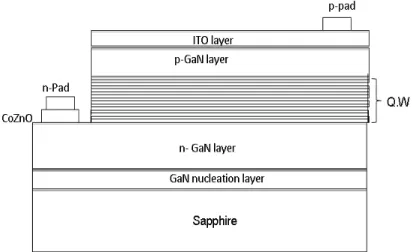
Figure 1 schematically depicts the configuration of a horizontal LED with a CZO film above the n-electrode pad. The LED samples that were used in this study were grown on c-plane (0001) sapphire substrates. On top of the sapphire substrate, a 25 nm-thick GaN nucleation layer was grown in H
. For a ZnO-based film that is grown on p-GaN or n-GaN to form GaN-based LEDs, the effect of the ZnO-based film on the output power of the LED has not yet been determined, to the best of our knowledge. This work demonstrates the application of Co-doped ZnO (CZO) films on n-GaN in GaN-based LEDs to increase current uniformity over that of standard LED chips. The use of the CZO layer is effective and promising for the enhancement of the LED output power for applications.
2 and NH3
ambient at 1100°C, and followed by a 2.8 μm-thick n-type GaN layer and a 20-period InGaN/GaN multiple-quantum-well (MQW). Subsequently, the Mg-doped p-type GaN cladding layer (~250 nm) was deposited. Finally, for a standard device, the ITO TCL film was formed on top of the p-GaN layer. The GaN layers and InGaN/GaN MQW were prepared by metal-organic chemical-vapor deposition (MOCVD) and molecular beam epitaxy (MBE), respectively.5,6,7
The CZO film was formed on the n-GaN layer by pulse layer deposition (PLD) at a base pressure of 1x10
-9
torr, before n-pad plating was performed. A KrF excimer laser (Coherent Inc made) with a wavelength of 248nm was used in PLD. Notably, the Co doping concentration and crystal quality of CZO is important to the current uniformity and enhancement of LED output power. To grow a high-quality CZO film, the growth temperature was controlled at 300。C and the oxygen pressure was maintained at 1x10⁻⁷ to 1x10⁻⁵ torr. The laser energy density was 1 J/cm2 and the repeat rate was 2Hz, resulting in a
growth rate of CZO film about 1.8nm/min. The quality of CZO films were in-situ characterized by reflection high energy electron diffraction (RHEED) and ex-situ studied by x-ray diffraction (XRD).
Fig. 1. Schematic structure of InGaN/GaN MQW LED with a Co-doped ZnO film deposited on n-GaN.
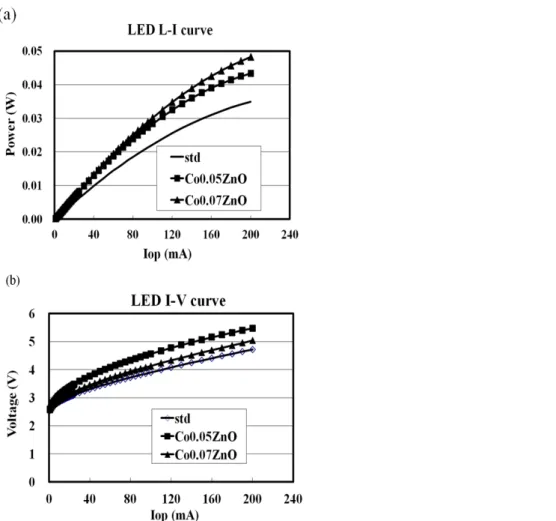
For chip processing and measurement, a device with an area 400×800 μm2 was fabricated using the standard LED procedure. The LED chip was then attached to a TO-18 can to measure the light output power in an integrating sphere. The I-V characteristics were measured using a Keithley 2420 meter. All optical and I-V measurements were made at room temperature. Figure 2(a) plots the output power current (L-I) for the LEDs without CZO and with Co(5%) and Co(7%)-doped CZO films. The corresponding values of output power were (34.9± 0.5), (43.3± 0.6) and (48.3± 0.7) mW, for an input current at (200± 1)mA. The application of the Co(5%) and Co(7%)-doped CZO films increased the output power by 24% and 38%, respectively. Figure 2(b) shows the forward voltage of the LEDs without CZO, with a Co(5%)-doped CZO film and with a Co(7%)-doped CZO film was (3.02±0.01), (3.36±0.01) and (3.13±0.01) V, respectively, for an input current at (200± 1) mA. Figure 3 compares statistics concerning the output power of standard LEDs with those obtained using the Co(5%) and Co(7%)-doped CZO films. The LEDs with Co(5%) and Co(7%)-doped CZO films improve the average output power up to 12.8% and 24.7%, respectively.
Fig. 2. L-I (a) and Vf –I (b) characteristics of standard LED and LEDs with Co(5%) and Co(7%)-doped CZO films using C2 electrode configuration.
Fig. 3. The output power of standard LED, and LEDs with Co(5%) and Co(7%) CZO films using C2 electrode configuration.
Near-field light intensity measurements were made to determine light intensity and current uniformity. Figure 4 shows those of the standard LED and the LED with Co(7%)-doped CZO film grown at 200-300。C. The light intensity of the LED chip with the Co(7%)-doped CZO film is much more uniform and higher than that on the standard LED chip. Notably, CZO films grown at low temperature (room temperature, RT) or excess doping of Co (>10%) in CZO does not improve the current uniformity and LED output power. In addition, the average LED output power change less than 5% between the standard LED and the LED with pure ZnO film.
Fig. 4. Light intensity profile of (a) standard LED chip without CZO film and (b) LED chips with Co(7%)doped CZO films (using C2 electrode configuration).
For CZO films grown at 200-300。C with Co doping concentration below 7%, high crystal quality and effective substitution of Co from Zn sites has been confirmed in our previous work.8,9 For excess doping of Co (>10%) or CZO films grown at RT, more structural defects might be formed and Co might segregate from the ZnO matrix and form nano particles10
It is known that the effective substitution of Co from Zn can result in the formation of impurity band
, as indicated by the RHEED, XRD and TEM studies (not shown here).
11,12
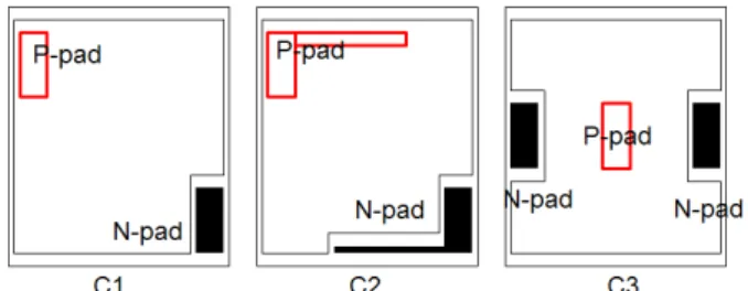
To study the effect of electrode configuration on LED performance, three types (C1, C2, C3) of finger electrode pad with the photo mask design were utilized in chips of a particular size 400×800 μm
near the conduction band minimum of ZnO. This is likely the key factor for the improvement of current injection and distribution and thus the enhancing output power of the GaN based LEDs using high quality CZO film.
2
, as shown in Fig. 5. The following study compares the LED chip with different type of finger electrode pads and Co doping concentration in CZO film. These GaN based LEDs were prepared in the same growth and the chip processing procedures.
Fig. 5. Three types (C1, C2 and C3) of LED finger electrode pad
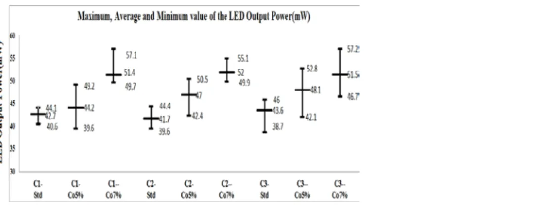
Twenty samples of each type of finger electrode pad were made for this study. Figure 6 shows the change of the average LED output power for three types of finger electrode pads. For the first type (C1), the average optical output power of a standard LED, and LEDs with Co(5%) and Co(7%) doped CZO film was (42.7±0.6), (44.2±0.7) and (51.4±0.8) mW, respectively, at an input current of (200±1) mA, and so the output power of LEDs with Co(5%) and Co(7%)-doped CZO film was 3.4% and 20.2% higher, respectively, than that of the standard LED. For the second type (C2), the corresponding average values of optical output power were (41.7±0.6), 47.0±0.7) and (52.0±0.8) mW, representing improvements of 12.8% and 24.7% for LEDs with Co(5%) and Co(7%) doped CZO film. For the third type (C3), the average values of optical output power were (43.6±0.6), (48.1±0.67) and (51.5±0.8) mW, respectively, representing improvements of 10.4% and 18.1% for LEDs with Co(5%) and Co(7%) doped CZO film.. Figure 6 shows the average output power of the LEDs with different CZO films and finger electrode configurations considered in this work.
Fig. 6. Average output power of LEDs with different CZO films and finger electrode configurations.
In general, C2 and C3 LED chips result in a better current distribution uniformity and LED output power than the C1 chips. The results further reveal that both current injection area and current path are important for the improvement of the current distribution uniformity and the output power of different types LED chips. Table 1 summarizes the LEDs output power with the different CZO films and finger electrode configurations. The output power of standard LED is about 40~49mW. The LEDs samples with Co(7%)-doped CZO film (C2 configuration) show noticeably larger output power than the standard LEDs.
Table 1. The LEDs output power distribution of samples with different CZO films and finger electrode configurations. In conclusion, the CoZnO films were deposited on an n-GaN layer before n-electrode pad plating. The use of Co doped CoZnO films effectively improved light output power compared to the standard LED. These findings are attributed to the improvement of current injection and of current distribution, which in turn likely due to the introduction of impurity band (near the conduction band minimum) in CZO. The electrode configuration can further affect the current injection area and current path and is useful for further improvement of the current distribution and the output power of GaN based LEDs. The approaches and results are very promising for applications.
The authors would like to thank the National Science Council of Taiwan, for financially supporting this research under Contract No. NSC_99-2120-M-006-003.
Reference
1. Hyunsoo Kim, Seong-Ju Park, Hyunsang Hwang, and Nae-Man Park, Appl. Phys. Lett. 81, 1326 (2002).
2. C.J. Tun, J. K. Sheu, M. L. Lee, C. C. Hu, C. K. Hsieh, and G. C. Chi, J. Electrochem. Soc., 153, G296 (2006).
3. Y. I. Alivov, B.Xiao, S. Akarca-Biyikli, H. Morkoc, D. Johnstone, O. Lopatiuk-Tirpak, L. Chernyak and W. Litton, J. Phys: Condens. Matter. 20, 085201 (2008).
4. J. K. Sheu, K. H. Chang, M. L. Lee, J. F. Huang, K.S. Kang, W. L. Wang, W. C. Lai and T. H. Hsueh, J. Electrochem. Soc., 156, H679 (2009).
5. C. L. Chao, R. Xuan, H. H. Yen, C. H. Chiu, Y. H. Fang, Z. Y. Li, B. C. Chen, C. C. Lin, C.H. Chiu, Y. D. Guo, H. C. Kuo, J. F. Chen, and S. J. Cheng, IEEE Photonic. Tech. Lett. 23, 798 (2011).
6. H. K. Cho , J. Y. Lee, N. Sharma , C. J. Humphreys, G. M. Yang, C. S. Kim, J. H. Song and P. W. Yu, Appl. Phys. Lett. 79, 2594 (2001).
7. Tao-Hung Hsueh, Jinn-Kong Sheu, Wei-Chi Lai, Yi-Ting Wang, Hao-Chung Kuo, and Shing-Chung Wang, IEEE Photonic. Tech. Lett. 21, 414 (2009).
8. J. C. A. Huang, H. S. Hsu, Y. M. Hu, C. H. Lee, Y. H. Huang, and M. Z. Lin, Appl. Phys. Lett. 85, 3815 (2004).
9. J. C. A. Huang and H. S. Hsu, Appl. Phys. Lett. 87, 132503 (2005).
10. H. S. Hsu, J. C. A. Huang, Y. H. Huang, Y. F. Liao, M. Z. Lin, C. H. Lee, J. F. Lee, S. F. Chen, L. Y. Lai, and C. P. Liu, Appl. Phys. Lett. 88, 242507 (2006).
11. J. M. D. Coey, M. Venkatesan and C. B. Fitzgerald, Nature Materials 4, 173 - 179 (2005). 12. M. Venkatesan, C. B. Fitzgerald, J. G. Lunney, and J. M. D. Coey, Physical Review Letters 93,
98 年度專題研究計畫研究成果彙整表
計畫主持人:黃榮俊 計畫編號: 98-2119-M-006-006-計畫名稱:新穎材料開發關鍵核心設施計畫--磊晶氮氧物材料成長的關鍵核心設施建置 量化 成果項目 實際已達成 數(被接受 或已發表) 預期總達成 數(含實際已 達成數) 本計畫實 際貢獻百 分比 單位 備 註 ( 質 化 說 明:如 數 個 計 畫 共 同 成 果、成 果 列 為 該 期 刊 之 封 面 故 事 ... 等) 期刊論文 0 0 100% 研究報告/技術報告 0 0 100% 研討會論文 0 0 100% 篇 論文著作 專書 0 0 100% 申請中件數 0 0 100% 專利 已獲得件數 0 0 100% 件 件數 0 0 100% 件 技術移轉 權利金 0 0 100% 千元 碩士生 2 2 100% 博士生 4 4 100% 博士後研究員 1 1 100% 國內 參與計畫人力 (本國籍) 專任助理 0 0 100% 人次 期刊論文 21 21 100% 研究報告/技術報告 0 0 100% 研討會論文 6 6 100% 篇 論文著作 專書 0 0 100% 章/本 申請中件數 0 0 100% 專利 已獲得件數 0 0 100% 件 件數 0 0 100% 件 技術移轉 權利金 0 0 100% 千元 碩士生 0 0 100% 博士生 0 0 100% 博士後研究員 3 3 100% 國外 參與計畫人力 (外國籍) 專任助理 0 0 100% 人次其他成果