Polymer space-charge-limited transistor as a solid-state vacuum tube triode
Yu-Chiang Chao, Ming-Che Ku, Wu-Wei Tsai, Hsiao-Wen Zan, Hsin-Fei Meng, Hung-Kuo Tsai, and Sheng-Fu Horng
Citation: Applied Physics Letters 97, 223307 (2010); doi: 10.1063/1.3513334
View online: http://dx.doi.org/10.1063/1.3513334
View Table of Contents: http://scitation.aip.org/content/aip/journal/apl/97/22?ver=pdfcov Published by the AIP Publishing
Articles you may be interested in
High output current in vertical polymer space-charge-limited transistor induced by self-assembled monolayer Appl. Phys. Lett. 101, 093307 (2012); 10.1063/1.4748284
Sensitive gas sensor embedded in a vertical polymer space-charge-limited transistor Appl. Phys. Lett. 101, 023303 (2012); 10.1063/1.4734498
Low voltage active pressure sensor based on polymer space-charge-limited transistor Appl. Phys. Lett. 95, 253306 (2009); 10.1063/1.3266847
Light-emitting polymer space-charge-limited transistor Appl. Phys. Lett. 93, 223301 (2008); 10.1063/1.3027057 Polymer space-charge-limited transistor
Appl. Phys. Lett. 88, 223510 (2006); 10.1063/1.2207838
This article is copyrighted as indicated in the article. Reuse of AIP content is subject to the terms at: http://scitation.aip.org/termsconditions. Downloaded to IP: 140.113.38.11 On: Wed, 30 Apr 2014 08:25:43
Polymer space-charge-limited transistor as a solid-state vacuum tube
triode
Yu-Chiang Chao,1Ming-Che Ku,2Wu-Wei Tsai,2Hsiao-Wen Zan,2,a兲 Hsin-Fei Meng,1,a兲 Hung-Kuo Tsai,3and Sheng-Fu Horng3
1
Institute of Physics, National Chiao Tung University, HsinChu 300, Taiwan
2
Department of Photonics and Institute of Electro-Optics, National Chiao Tung University, HsinChu 300, Taiwan
3
Institute of Photonics Technologies, National Tsing Hua University, Hsinchu 300, Taiwan
共Received 10 June 2010; accepted 17 October 2010; published online 3 December 2010兲
We report the construction of a polymer space-charge-limited transistor 共SCLT兲, a solid-state version of vacuum tube triode. The SCLT achieves a high on/off ratio of 3⫻105at a low operation voltage of 1.5 V by using high quality insulators both above and below the grid base electrode. Applying a greater bias to the base increases the barrier potential, and turns off the channel current, without introducing a large parasitic leakage current. Simulation result verifies the influence of base bias on channel potential distribution. The output current density is 1.7 mA/cm2with current gain greater than 1000. © 2010 American Institute of Physics.关doi:10.1063/1.3513334兴
Since the late 19th century, scientists have researched technologies that provide electronic switch and signal ampli-fier. The vacuum tube is a triode with a hot cathode, plate anode, and a controlling grid inside an evacuated glass tube. Since its patent in 1906, the vacuum tube became a dominant technology until the rise of the transistor, at around 1960. Yet even today, vacuum tubes survive in specialist areas, includ-ing high-power applications, audio amplifiers, and in military applications due to its resistance to electromagnetic pulse. Aside from these practical applications, the vacuum tube is elegant in both structure and operation principle. It is thus interesting to ask whether the vacuum tube concept can see a revival in this era of solid-state electronics, and once again prove its unique advantages.
Attempts during the 1950s and 1960s, to build vacuum tubes using inorganic semiconductors, proved unsuccessful because of difficulties with the dopant diffusion process in forming the grid structure.1–3 Several reports, since the 1990s, describe research into intrinsic organic semiconductor designs that deliver vacuum tube functionality.4,5Fabrication of the grid, by deposition through a shadow mask, with openings on the micron-scale, results in poor current density and on/off ratio.4Improvements in grid design, using high-density nanometer scale openings increased output current density to greater than 1 mA/cm2,6–8sufficient for most ap-plications. The difficulty regarding the on/off ratio of solid-state vacuum tubes lies in the large spatial overlap between the grid and collector electrode. In an early solid-state device design,7the on/off ratio was only 102; recently we raised it to 104 by introducing an insulator to surround the grid.9
A key challenge to the development of a solid-state version of the vacuum tube is to raise the on/off ratio to around 105, this being the generally accepted ratio required for practical applications.10 For example, in the switching transistor for a sensor array with 1000 lines, the current readout is the sum of the currents for one line in the on-state, and 999 lines in the off state. The latter must be one order of magnitude smaller than the range of variation of the former, which is
usually ten times. The transistor on-current must therefore be at least 105times larger than the off-current.10
In this study, we attained an on/off ratio of 3⫻105 by simply increasing the thickness of the insulator between the emitter and the grid. The greater thickness allows a wider range of grid po-tentials able to modulate the collector current before break-down occurs. With this final improvement, the solid-state vacuum tube offers superior performance features compared to its field-effect transistor counterpart, with lower voltage, higher output current, and comparable on/off ratio.
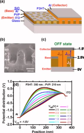
We named our solid-state version of the vacuum tube triode a “polymer space-charge-limited transistor” 共SCLT兲. Figure 1共a兲 shows a schematic diagram of the device and Fig.1共b兲is a scanning electron microscopy共SEM兲 image of the openings form at sites without Al. In operation, the holes are injected into organic semiconductor by the emitter, and are collected by the collector. The emitter-collector diode’s space-charge-limited current 共SCLC兲 is modulated by a metal base electrode embedded within the semiconductor. The voltages applied to the collector and base, determine a potential barrier between the emitter and collector. The SCLT on and off states are determined by whether carriers encoun-ter a high or low potential barrier. Simulation for the pro-posed SCLT device were carried out with Silvaco TCAD
ATLASsoftware. Simulation parameters are given in Ref. 11. Figure 1共d兲 shows a simulated potential distribution at the central vertical channel when collector-to-emitter voltage 共VCE兲 is –1.5 V and base-to-emitter voltage 共VBE兲 varies from 2.5 to –2.5 V. The figure describes a strong bias effect on potential distribution. A more positive VBEleads to a higher potential barrier to turn off the channel current. A simulated channel current density JCEversus VBEplot, for VCEequal to –1.5 V reveals that, in the absence of all parasitic leakage, the device on/off current ratio could be greater than nine orders of magnitude.
Figure1共c兲depicts origins of the SCLT off-current. At a fixed negative VCE, the output collector current density共JC兲 is the sum of JC1 and JC2. JC1 is the current density from emitter to collector, JC2 is the leakage current density from base to collector, and J3is the leakage current between base and emitter. The arrows indicate the direction of current. a兲Authors to whom correspondence should be addressed. Electronic
ad-dresses: [email protected] and [email protected].
APPLIED PHYSICS LETTERS 97, 223307共2010兲
0003-6951/2010/97共22兲/223307/3/$30.00 97, 223307-1 © 2010 American Institute of Physics This article is copyrighted as indicated in the article. Reuse of AIP content is subject to the terms at: http://scitation.aip.org/termsconditions. Downloaded to IP:
Tuning the VBE from negative to positive suppresses JC1, however, JC2 and J3 both increase, since the voltage drop across the base and collector 共VBC兲, and VBE are increased. The minimum of JCis reached as JC2becomes comparable to
JC1. Hence, in order to maximize the on/off ratio, while keeping the current gain high, ways to reduce JC2 and J3 must be found. We added a 50 nm insulating SiO layer above the base electrode, and increased the thickness of the PVP insulating layer below the base electrode to 210 nm. We demonstrate a polymer vertical transistor with enhanced in-sulating properties of the inin-sulating layers, which allows a high VBE and makes a high on/off ratio of 3⫻105 possible. The SCLT was fabricated on indium tin oxide 共ITO兲 glass substrate which was plasma cleaned with 150 W O2 plasma for 30 min to smooth the substrate. A 210 nm thick layer of cross-linkable PVP was spin coated onto the ITO substrate, and then cross-linked at 200 ° C for 60 min under an inert atmosphere, and using methylated poly共melamine-co-formaldehyde兲 共Aldrich, Mw⬃511兲 as a cross-linking agent. The PVP surface was made hydrophilic by 50 W O2 plasma treatment, and then submerged into 210 nm diameter positively charged polystyrene 共PS兲 spheres 共Merck, K6-020兲 in dilute ethanol solution 共0.8 wt % PS兲 for three min-utes. The PS spheres adsorbed to the PVP surface to serve as the shadow mask. The substrate was then transferred to a beaker of boiling isopropanol solution for 10 s, to form two-dimensional colloidal arrays, and immediately blown dry in a
stream of nitrogen gas. A 40 nm thick layer of Al, and 50 nm layer of SiO were deposited atop the PVP layer, to form the metal base electrode and upper insulator, respectively. After removing the PS spheres with adhesive tape 共Scotch, 3M兲, PVP material at sites without Al coverage was removed by O2plasma treatment at 150 W for 13 min. In a glove box, a 350 nm poly共3-hexylthiophene兲 共P3HT兲 layer was spin coated onto the substrate from 4.5 wt % chlorobenzene solu-tion. Finally, the aluminum collector material was deposited to complete the SCLT with a 1 mm2 active area.
Figure2共a兲shows insulating properties of PVP layers of various thicknesses. The 210 nm PVP device exhibited lower leakage current density than the 60 nm device. The enhanced insulating properties of 210 nm PVP allow the emitter-base diode to sustain higher bias without breakdown. In order to improve the SCLT characteristics, the P3HT layer should be no thinner than the upper surface of the base, and depres-sions in the P3HT surface should not be observable in SEM images above the base opening sites.12 Since we formed a 210 nm PVP layer, the P3HT layer must be thicker than 210 nm. Thus, we fabricated diodes in the ITO/P3HT/Al struc-ture with various P3HT thicknesses, in order to understand the diode characteristics. The current densities of these di-odes were recorded with 2.5 V applied on ITO emitter, and carrier mobility’s were deduced from the currents follow SCLC. As shown in Fig.2共b兲, current density decreases with increasing P3HT thickness, however, carrier mobility in-creases with increasing P3HT thickness. This phenomenon was also observed in small molecule organic diodes.13,14The authors concluded that the organic thin film’s low mobility originated from an interfacial trap state, and molecular ar-rangement on the surface. In our case, since P3HT is known to be sensitive to surface conditions, the molecular orienta-tion condiorienta-tion in the region close to the ITO must differ from
FIG. 1.共Color online兲 共a兲 Schematic diagram of SCLT device structure. 共b兲 SEM image of openings formed at sites without Al grid prior to spin coating with P3HT. The white scale bar indicates 200 nm.共c兲 Three current sources in SCLT. JC1is the current density from emitter to collector, JC2is the leakage current density from grid to collector, and J3is the leakage current density between emitter and collector.共d兲 A simulated potential distribution at the central vertical channel. Higher base-bias leads to a higher potential barrier.
FIG. 2. 共Color online兲 共a兲 J-V characteristics of insulating PVP layer of various thicknesses. The device structure is ITO/PVP/Al.共b兲 Current density at 2.5 V for diodes with various P3HT thicknesses. The device structure is ITO/P3HT/Al. Carrier mobility of each diode was obtained from the SCLC.
223307-2 Chao et al. Appl. Phys. Lett. 97, 223307共2010兲
This article is copyrighted as indicated in the article. Reuse of AIP content is subject to the terms at: http://scitation.aip.org/termsconditions. Downloaded to IP: 140.113.38.11 On: Wed, 30 Apr 2014 08:25:43
that of the bulk far away from the ITO. The influence of interfacial conditions on the diode characteristics is becomes weaker as the thickness of P3HT increases, and hence the mobility of P3HT increases with increasing thickness.
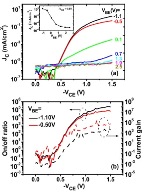
Figure3shows SCLT transistor characteristics. The inset of Fig. 3共a兲 shows the transfer characteristics of SCLT as determined from Fig. 3共a兲. The ITO emitter was grounded and the Al collector was negatively biased at VCE. If VCE equal to –1.5 V, then when VBEis –1.1 V, the SCLT is in the on state, and JCis 1.71 mA/cm2. When VBEis +2.5 V, JCis suppressed and the SCLT is in the off state. The base current density 共JB兲 is in the order of 10−4– 10−5 mA/cm2. Figure
3共b兲 shows on/off ratio and current gain of SCLT as func-tions of VCE. The on/off ratio is obtained by dividing JC共VBE at –1.1 or –0.5 V兲 by JC共VBE at 2.5 V兲. The current gain is obtained by dividing JCby JBwhen VBEis –1.1 or –0.5 V. As
VCE is –1.5 V, the maximum on/off ratio of 3⫻105 is achieved, and the current gain is still greater than 1000. This on/off ratio is larger than our previous work,8,10 and is the highest value so far reported for polymer vertical transistors. Since the transistor on current is in the same order as in our previous report, the improved on/off ratio must arise from the reduced off current, which may come from two sources. One is that applying a more positive VBEvoltage to the base can improve the on/off ratio. Using high quality insulators both above and below the grid base electrode is the key factor to enhancing the on/off ratio. The other is that the ratio of emitter-to-base thickness to the opening diameter is greater than that used in our previous work. Better grid con-trol is obtainable with a higher ratio.
We integrated a second SCLT in series with a load resis-tor 共RL= 10 M⍀兲, to demonstrate a resistive-load inverter operating at low supply voltages as shown in Fig.4. The VDD
was fixed at –2.5 V while input voltage共Vin兲 was varied from –1 to 1.5 V. When Vinwas 1.5 V, the SCLT is in the off state, the effective resistance from emitter to collector 共REC兲 is high, and hence the output voltage 共Vout兲 should approach
VDD. By contrast, when Vin is –1 V, the SCLT is in the on state, REC is low, and hence the Vout should approach zero. However, Voutis not close to 0.0 V when the SCLT is turned on. Increasing the output current when SCLT is in the on state can solve the problem. The absolute value of voltage gain is 3.3, higher than in our previous report.
In summary, we report the fabrication and operation of a SCLT with high on/off ratio and low operation voltage. By improving the insulator characteristics, a greater VBE bias at the base is possible for suppression of the off current. The demonstration of an inverter application illustrated a possible application for organic electronics devices with low power consumption.
This work was supported by the National Science Coun-cil of Taiwan under Contract No. NSC98-2628-M-009-001.
1W. Shockley,Proc. IRE 40, 1289共1952兲.
2S. A. Roosild, R. P. Dolan, and D. O’Neil,Proc. IEEE 51, 1059共1963兲. 3S. Teszner and R. Gicquel,Proc. IEEE 52, 1502共1964兲.
4K. Kudo, D. X. Wang, M. Iizuka, S. Kuniyoshi, and K. Tanaka,Thin Solid
Films 331, 51共1998兲.
5Y. Yang and A. J. Heeger,Nature共London兲 372, 344共1994兲.
6K. Fujimoto, T. Hiroi, and M. Nakamura,e-J., Surf. Sci. Nanotechnol 3, 327共2005兲.
7Y. C. Chao, H. F. Meng, S. F. Horng, and C. S. Hsu,Org. Electron.9, 310 共2008兲.
8K. Fujimoto, T. Hiroi, K. Kudo, and M. Nakamura,Adv. Mater. 19, 525 共2007兲.
9Y. C. Chao, Y. C. Lin, M. Z. Dai, H. W. Zan, and H. F. Meng,Appl. Phys.
Lett. 95, 203305共2009兲.
10T. Someya, Y. Kato, T. Sekitani, S. Iba, Y. Noguchi, Y. Murase, H. Kawaguchi, and T. Sakurai, Proc. Natl. Acad. Sci. U.S.A. 102, 12321
共2005兲.
11The SCLT characteristics simulation is made based on the device structure shown in Fig.1共c兲. Insulator surrounds the grid is used to make the model more realistic. The thickness of PVP, Al grid, and P3HT are 200 nm, 40 nm, and 350 nm, respectively. The opening diameter is 210 nm. The high-est occupied molecular orbital and lowhigh-est unoccupied molecular orbital levels of P3HT are 5.2 and 3.0 eV. The work function of emitter and collector are 5.2 and 4.3 eV. The hole mobility and electron mobility are 10−5and 10−6 cm2/V s.
12Y. C. Chao, C. Y. Chen, H. W. Zan, and H. F. Meng,J. Phys. D: Appl.
Phys. 43, 205101共2010兲.
13T. Y. Chu and O. K. Song,Appl. Phys. Lett. 91, 073508共2007兲. 14T. Y. Chu and O. K. Song,J. Appl. Phys. 104, 023711共2008兲.
0.0 0.5 1.0 1.5 10-3 10-2 1010-1 0 101 102 103 104 105 106 10-5 10-3 10-1 101 103 105 107 109 On/o ff rati o -VCE(V) -1.10V -0.50V VBE= Current gain -1 0 1 2 3 10-6 10-4 10-2 100 -VCE=1.5V JC ( mA/ cm 2) VBE(V) 0.0 0.5 1.0 1.5 10-7 10-5 10-3 10-1 101 2.5 1.9 1.3 0.7 0.1 -0.5 VBE(V)= JC (mA/ cm 2 ) -VCE(V) -1.1 (a) (b)
FIG. 3.共Color online兲 共a兲 JCas a function of VCEunder various VBEvalues. The inset shows the transfer characteristics of SCLT for VCE⫽–1.5 V. 共b兲 On/off ratio and current gain as a function of VCE.
FIG. 4. 共Color online兲 Transfer characteristics and gain of the inverter at VDDof –2.5 V. The load resistance is 10 M⍀. The inset shows the sche-matic inverter circuit.
223307-3 Chao et al. Appl. Phys. Lett. 97, 223307共2010兲
This article is copyrighted as indicated in the article. Reuse of AIP content is subject to the terms at: http://scitation.aip.org/termsconditions. Downloaded to IP: 140.113.38.11 On: Wed, 30 Apr 2014 08:25:43