Abstract— Nitride-based light-emitting diodes (LEDs) grown
with a structure of InN/GaN matrix quantum-wells (QWs) using metal–organic chemical vapor deposition are fabricated and characterized. The InN/GaN matrix QWs can significantly enhance the formation of phase-separated In-rich regions. Under an injection current of 500 A/cm2, the LED output power can be enhanced by 26%, and the efficiency droop can be improved as compared with a conventional LED. These improvements could be attributed to the strong localization effect to remove carriers from the confining potential and capture these carriers at nonradiative centers in the active layer.
Index Terms— InN/GaN, efficiency droop, In rich, localization
effect.
I. INTRODUCTION
G
aN and its related compounds, such as AlGaN and InGaN, have emerged as important semiconductor mate-rials for high-performance light emitters in the ultraviolet (UV), blue, and green spectral regions [1], [2]. To determine feasible solid state lighting, LED output efficiency must be further improved. However, efficiency droop is a fundamen-tal problem in InGaN-based high-power LEDs. Numerous researchers have recently reported that efficiency droop can be attributed to carrier delocalization from In-rich regions [3]–[5]. Yang et al. suggested that the overflow of carriers from localized states appears to be the major mechanism of the droop [6]. The localization effects might serve a major func-tion in the improvement of radiative efficiency by enhancing electron-hole overlap and by preventing carriers from reaching dislocations.Some methods such as the addition of InN interfa-cial layers between the quantum-wells and the barriers, trapezoid/triangular QWs, asymmetric two-step SQW with In0.08Ga0.92N shallow step, and pulsed TMIn-treated QWs have recently been reported to improve the internal quantum efficiency of InxGa1−xN-GaN multi-quantum well (MQW) LEDs [7]–[10]. Such methods result to interface improve-ment and the formation of In-rich regions for strong Manuscript received December 15, 2013; revised February 7, 2014; accepted February 16, 2014. Date of publication February 20, 2014; date of current version February 26, 2014. This work was supported by the National Science Council of Taiwan under Grants NSC 101-2221-E-009-028-MY3 and NSC-3113-P-009-007-CC2.
C. H. Kuo, L. C. Chang, and Y. A. Chen are with the Institute of Lighting and Energy Photonics, National Chiao Tung University, Tainan 71150, Taiwan (e-mail: [email protected]; [email protected]).
Y. K. Fu is with the Opto-Electronics Epitaxy and Device Department, Industrial Technology Research Institute, Hsinchu 31040, Taiwan (e-mail: [email protected]).
Color versions of one or more of the figures in this paper are available online at http://ieeexplore.ieee.org.
Digital Object Identifier 10.1109/JQE.2014.2306997
localizing carrier. H. Zhao reported the use of delta InN layer to enabling strong localization of the electron wavefunction within the InGaN QWs, which will be useful in achieving improved optical matrix elemenets for addressing the charge separation issue in InGaN-based LEDs [11]–[13]. Recently, Yoshikawa et al. demonstrated the fabrication of InN/GaN MQW consisting of one monolayer (ML) and a fractional ML InN well inserted in a GaN matrix under In-polarity growth regime by radio frequency plasma assisted molecular beam epitaxy [14]. The critical thickness of InN epitaxy on GaN is approximately 1 ML, and the growth temperature for 1 ML InN insertion can be remarkably higher. Thus, the proposed MQW structure can avoid or reduce the generation of misfit dislocation, resulting in a higher quality MQW-structure nature in principle than that of former InN-based MQWs [15].
In this study, nitride-based LED is fabricated with InN/GaN matrix QWs. Electro-optical properties of the fabricated LEDs will also be discussed. Compared with the conventional InGaN MQW LED, the LED with InN/GaN matrix QWs can improve the light output power and efficiency droop.
II. EXPERIMENT
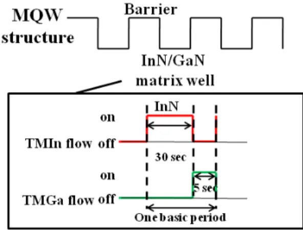
The LED samples used in this study were all grown on 2 in sapphire (0001) substrates using a Thomas Swan MOCVD system. Details of the growth procedures can be found elsewhere [16], [17]. Conventional LED and LEDs with InN/GaN matrix well layers were prepared. The conventional LED, labeled as LEDI, consists of a 30 nm thick GaN nucle-ation layer, a 2.0 μm thick unintentionally doped GaN layer, a 2.5 μm thick Si-doped GaN layer, an InGaN/GaN MQW active region, and a 0.3 μm thick Mg-doped GaN layer. The MQW active region consists six periods of 3 nm thick InGaN well layers and 12 nm thick GaN barrier layers. The TMGa, TMIn and NH3 flow rate was set at 2.78 umole/min, 6.49 umole/min and 0.22 mole/min, respectively. The growth temperature and pressure was nearly 777 °C and 400 mbar, respectively. We simultaneously introduced TMIn, TMGa and NH3into the growth chamber for 105 s during the growth of the 3-nm-thick InGaN well layers. For LEDs with InN/GaN matrix, QWs were also fabricated. Instead of the 3 nm thick InGaN well layers, InN/GaN matrix well layers were inserted for the InN/GaN matrix QW LED. The flow sequence of InN/GaN matrix-well layer was shown in Fig. 1. In one of the basic periods of the InN/GaN well layers, the TMIn and TMGa were introduced alternately with constant NH3flow. All the flow rate of MO sources, growth temperature and growth pressure used in the InN/GaN well layer were the same as the conventional InGaN well layer.
0018-9197 © 2014 IEEE. Personal use is permitted, but republication/redistribution requires IEEE permission. See http://www.ieee.org/publications_standards/publications/rights/index.html for more information.
Fig. 1. Time sequence of InN/GaN of flow-modulated growth method. The growth times of InN and GaN were 30 and 5 s, respectively. After depositing 11 periods of this basic structure, a 12 nm thick GaN barrier layer was also deposited. The InN/GaN matrix QWs are called as LEDII. However, the 30 s InN deposition under the growth temperature of 777 °C cannot form one monolayer (ML) InN. GaN growth will effectively increase the bonding strength between In and N, thereby reducing the desorption of In [14]. The 5 s GaN deposition cannot cover the entire surface. Therefore, a fractional InGaN ML was formed after one InN/GaN growth. 11 InN/GaN switchings are needed to form 3nm InGaN wells. InN growth plays a role similar to that of the In surfactant treat-ment during the InN/GaN growth switching of InGaN wells [18]–[20]. Both the growth rates of InN and GaN in one period are very difficult to define. The structural properties of the two LEDs were then evaluated using double crystal X-ray diffraction on a Bede D1 system. Cross-sectional transmission electron microscopy (TEM) in a FEI Tecnai G2 F20 system was also used to reveal In-rich distributions of MQW structure. Temperature-dependent PL experiments were performed using a 25 mW He-Cd laser operated at 325 nm as the pumping source, and the samples were mounted on a helium close loop cryostat during measurements.
For the fabrication of LEDs, the surface of the samples was partially etched until the n-type GaN layers were exposed. LEDs with Al-doped ZnO serving as a transparent contact layer were fabricated [21]. Cr/Au was subsequently deposited onto the exposed n-type GaN layer to serve as the n-type electrode. The chip size of LED was 300 μm × 300 μm. The chips were subsequently packaged into lamps. Intensity-current (L-I) characteristics of the packaged lamps were subsequently measured using the molded LEDs with the integrated sphere detector. To minimize heating further under high current injection, the samples were mounted on a heat sink with thermoelectric cooling during measurements. The injection current was a pulsed current source with a 1% duty cycle and a frequency of 10 kHz.
III. RESULTS ANDDISCUSSION
Fig. 2 shows the (0002) 2θ-ω HRXRD patterns of LEDI and LEDII. The indium composition profile was calculated to
Fig. 2. The (0002) reflection of HRXRD 2θ-ω scans measured from the six-pairs of the LED I and LEDII.
Fig. 3. Cross sectional HRTEM image obtained from the MQW of (a) LED I and (b) LEDII.
be∼16% for LEDI and ∼17% for LEDII. The strongest peaks are from the thick GaN layer. The clear satellite peaks up to the fourth order, which indicate very abrupt interfaces between QW and QB, were observed in LEDI and LEDII.
Fig. 3(a) and (b) show TEM images of LEDI with con-ventional InGaN well and LEDII with InN/GaN matrix well, respectively. The inset of Fig. 3 are shown the enlarge figure observed the QW thickness. A number of dark spots in the InN/GaN matrix well layer were observed in LEDII. By contrast, the dark spots were significantly smaller for LEDI with conventional InGaN well, as shown in Fig. 3(a). Such an observation indicates that the InN/GaN matrix well can signif-icantly enhance phase separation and inhomogeneous indium distribution in the active layer. These In-rich regions can act as radiative recombination centers of GaN-based LEDs. However, the In-rich region will cause the lattice mismatch between QW and QB. The increased roughness for LED II was observed in Fig. 3(b).
Indium phase separation and composition fluctuation were known to be related to the biaxial strain in InGaN layer grown on GaN and also to the miscibility gap between InN and GaN, which can shift notably into high In-content regime of the temperature composition diagram [22]–[25]. Based on the energy balance model [26], [27], the critical layer thickness of the InGaN/GaN bilayer structure is estimated to be 50 nm for an indium composition of 17% as in our experiment. Because the thickness of the QW layer in LEDI is about 3 nm, the InGaN layer is grown on GaN under compressive strain. Therefore, phase separation would not be expected to occur due to coherence strain [24]. However, the phase separation in InGaN layers can be enhanced under some conditions such as on a rough surface [28] or using an antisurfactant
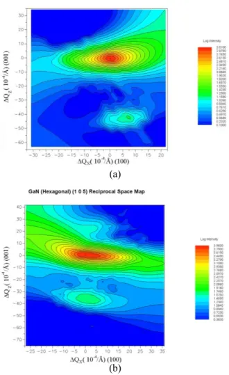
Fig. 4. X-ray RSM for the (105) reflection of the (a) LED I and (b) LEDII. Two diffraction peaks correspond to the GaN and the InGaN, respectively. It shows that the LED I has large degree strain relaxation.
in the growing procedure of InGaN layer [29]. To clear the effect of nanostructure formation of InN/GaN matrix QW on enhancing phase separation, a strain analysis is performed using x-ray RSM. The asymmetrical x-ray RSM for the (105) reflection of the LEDI and LEDII is shown in Fig. 4(a) and (b), which confirms that the InN/GaN matrix QWs has the state of partially relaxation. Therefore, the formation of nanostructure with LEDI structure is believed to relieve the compressive strain and enhance the phase separation, thus permitting self-assembled In-rich QDs to be formed in QW layers.
The Fig. 5(a) shows the 20 mA (22.2 A/cm2) electrolu-minescence (EL) spectra of the fabricated LEDs. With an injection current of 22.2 A/cm2, the EL peaks were found to be 446 and 444 nm, whereas full-width at half-maxima (FWHM) were 19 and 24 nm for LEDI and LEDII, respec-tively. Compared with LED I, the larger EL FWHM observed from LED II could be attributed to the fact that the InN/GaN matrix well could provide inhomogeneous indium distribution in the well layer. Fig. 5(b) shows the light output power and external quantum efficiency (EQE) as a function of injection current for two LEDs. With a 500 A/cm2 current injection, LED output powers were 71.0 and 89.4 mW for LEDI and LEDII, respectively. Compared with LEDI, the LED output
Fig. 5. (a) the normalized EL intensity for the two fabricated LEDs with 20 mA injection current. (b) EQE and output power versus injection current density for the two fabricated LEDs.
power could be enhanced by 26% at a current density as high as 500 A/cm2 for LEDII. Improvement of efficiency droop is observed for LEDII. Compared with the EQE at an injection current of peak value, the EQE values at an injection current of 500 A/cm2 are approximately reduced by 47% and 21% for LEDI and LEDII, respectively. We propose that the improvement of LED output power and efficiency droop should be attributed to the more significant localized states and quantum confinement in LEDII because of the formation of In-rich regions and better interfacial quality. This condition can reduce the carriers out of a confining potential to be captured at non-radiative centers in the active layer under high-injection current rather than thermal heating.
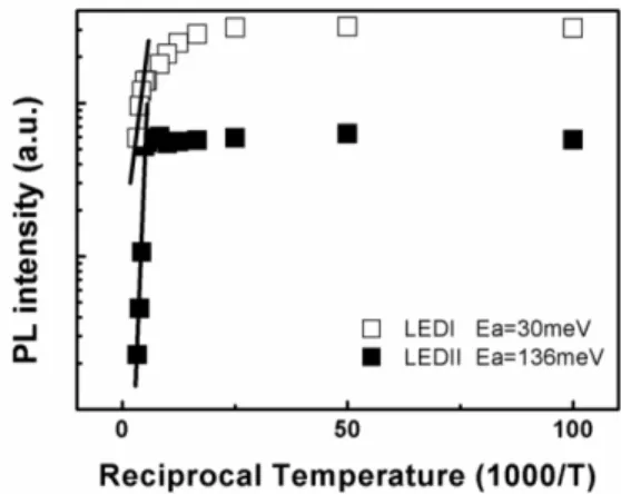
To clarify the reason for the enhancement of LED output power and the minor EQE droop effect in the InN/GaN matrix QW LED, temperature-dependent PL measurements were performed. Fig. 6 shows the Arrhenius plot of the integrated PL intensity of the two fabricated LEDs obtained from the main emission peak over the temperature range from 10 K to 300 K. The integrated PL intensity dropped slowly with temperature in the low-temperature region, but decreased rapidly in the high-temperature region. The best fitting gives two activation energies of approximately 30 and 136 meV for LEDI and LEDII, respectively. The thermal quench of PL intensity with temperature can be explained through the thermal emission of the carriers out of the confining potential
Fig. 6. The Arrhenius plot of the integrated PL intensity of the two fabricated LEDs obtained from the main emission peak over the temperature range from 10 to 300 K.
with activation energy to be captured at non-radiative centers in the active layer [30]. Such an enhancement in the activation energy could be attributed to the degrees of carrier confinement potential in the active layer that are more significant for LEDII compared with LEDI. This enhancement originated from the In-rich regions because of the InN/GaN matrix well. These In-rich regions are believed to behave in a similar manner as In-rich quantum dots in the active layer, providing deep potential wells that suppress the diffusion of electrical carriers toward various non-radiative defects. The carrier localization within In-rich regions in the active layer also significantly affects the performance of LEDs, resulting in an increase in radiative recombination efficiencies [31]. Therefore, the improvement of activation energy could prevent the carriers out of a confining potential to be captured at non-radiative centers under high injection current.
We believed the reason of lower IQE of LEDII is attributed to carrier transportation from the degree of phase separation. We considered there are two different indium contents existed in InN/GaN matrix QWs. As the temperature increases from 200 to 300K, the most carriers could move easily from high indium content to low indium content part by thermal emission because of the small energy difference among different indium content parts. At 300K, the PL emission is dominant by low indium contents region. The lower PL intensity of LEDII at 300K is attributed to the lesser low indium content densities. However, the mechanisms are still unknown. The actual rea-sons are needed to investigate further.
In the blue and green LEDs, the radiative recombination is enhanced by localization effects in nanoscale In-rich regions. As current injection is increased, band filling of the localized states followed by the screening of localized potentials will result in the releasing of electrons to the conduction band. The electrons can therefore move to the defects nearby and recombine nonradiatively with injected holes, leading to a decreased EQE. This interpretation is supported by the fact that the EQE droop is accompanied by a monotonic peak blue shift and spectral broadening up to 700 mA, both indicative of band filling of localized states. On the other hand, the radiative recombination in the UV LED is dominated by band-to-band transition due to the lack of localization effects [6].
Fig. 7. 5× 5 μm2AFM images of surface of a GaN layer deposited upon (a) conventional QW and (b) InN/GaN matrix well.
Therefore, defects have a significant influence on its per-formance, especially at low injection level. As defects are saturated at high currents, the EQE attains a saturation value. However, while the LEDs on GaN substrate are of better quality and more efficient, they exhibit similar efficiency droop behaviors. This finding confirms that dislocations are not responsible for the decrease in EQE of InGaN LEDs at elevated currents [3]. the carriers overflowing from localized states are lost at misfit defects in the QW regions and at the well/barriers interfaces rather than threading dislocations. As In content increases, the material quality of InGaN alloys degrades due to increasing phase separation as well as mis-match between the InGaN QW layers and GaN barrier layers. A large number of misfit defects may form at interfaces as strain is relieved, acting as nonradiative recombination centers. Compared to threading dislocations, the interfacial misfit defects can be more readily reached by the overflowed carriers. In this study, the InN/GaN matrix QW can enhance the phase separation to form self-assembled In-rich QDs in QW layers. Many misfit defects may form at interfaces but not observe from out InN/GaN matrix structure confirmed by XRD measurement. In order to inspect the crystal quality of QW, Fig. 7 shows the AFM images of sample A and B. These sample structures were same to LED samples, but
p-type GaN layers were not grown in order to obtain
disloca-tions densities (DDs) images from the active layers. These samples were annealed at the growth temperature of the
p-type GaN layer (1000 °C) after epitaxial growth to observe
the influence of growing the p-type GaN layers. The DDs were (a) 1.0 × 109 cm−2 and (c) 5.2× 108 cm−2. This method could obtain good quality of QW and provide high activation energies suppress the diffusion of electrical carriers toward various non-radiative defects under high injection current.
IV. CONCLUSION
In summary, this paper reported the application of InN/GaN matrix well structure as an active layer and demonstrated the effect of the application on emission properties. At 500 A/cm2 current injection, the output power of LEDII exhibited a 26% enhancement compared with LEDI. The droop effect can be drastically reduced to less than 21% at a current density of as high as 500 A/cm2. The improvement in output power and the reduction in efficiency droop of the InN/GaN matrix QW LED can result in enhanced localization effects and improved carrier confinement in the active region. Carriers out of the confining potential could be avoided to be captured at non-radiative centers in the active layer under high injection current.
[3] X. A. Cao, Y. Yang, and H. Guo, “On the origin of efficiency roll-off in InGaN-based light-emitting diodes,” J. Appl. Phys., vol. 104, no. 9, pp. 093108-1–093108-4, Nov. 2008.
[4] B. Monemar and B. E. Sernelius, “Defect related issues in the ‘current roll-off’ in InGaN based light emitting diodes,” Appl. Phys. Lett., vol. 91, no. 18, pp. 181103–181105, Oct. 2007.
[5] K. Akita, T. Kyono, Y. Yoshizumi, H. Kitabayashi, and K. Katayama, “Improvements of external quantum efficiency of InGaN-based blue light emitting diodes at high current density using GaN substrates,” J. Appl. Phys., vol. 101, no. 3, pp. 033104-1–033104-5, Feb. 2007.
[6] Y. Yang, X. A. Cao, and C. Yan, “Investigation of the nonthermal mechanism of efficiency rolloff in InGaN light-emitting diodes,” IEEE Trans. Electron Devices, vol. 55, no. 7, pp. 1771–1775, Jul. 2008. [7] Y. C. Cheng, C. M. Wu, M. K. Chen, C. C. Yang, Z. C. Feng,
G. A. Li, et al., “Improvements of InGaN/GaN quantum-well interfaces and radiative efficiency with InN interfacial layers,” Appl. Phys. Lett., vol. 84, no. 26, pp. 5422–5424, Jul. 2004.
[8] M. G. Cheong, C. Liu, H. W. Choi, B. K. Lee, E.-K. Suh, and H. J. Lee, “Study of the origin of luminescence in high indium composition InGaN/GaN quantum wells,” J. Appl. Phys., vol. 93, no. 8, pp. 4691–4695, Apr. 2003.
[9] C. H. Kuo, Y. K. Fu, C. L. Yeh, C. J. Tun, P. H. Chen, W. C. Lai, et al., “Nitride-based asymmetric two-step light-emitting diode with In0.08Ga0.92N shallow step,” IEEE Photon. Technol. Lett., vol. 21, no. 6, pp. 371–373, Mar. 15, 2009.
[10] T. H. Hsueh, J. K. Sheu, W. C. Lai, Y. T. Wang, H. C. Kuo, and S. C. Wang, “Improvement of the efficiency of InGaN–GaN quantum-well light-emitting diodes grown with a pulsed-trimethylindium flow process,” IEEE Photon. Technol. Lett., vol. 21, no. 7, pp. 414–416, Apr. 1, 2009.
[11] H. Zhao, G. Liu, and N. Tansu, “Analysis of InGaN-delta-InN quantum wells for light-emitting diodes,” Appl. Phys. Lett., vol. 97, no. 13, pp. 131114-1–131114-3, Oct. 2010.
[12] H. Zhao, G. Liu, J. Zhang, J. D. Poplawsky, V. Dierolf, and N. Tansu, “Approaches for high internal quantum efficiency green InGaN light-emitting diodes with large overlap quantum wells,” Opt. Exp., vol. 19, no. S4, pp. A991–A1007, Jul. 2011.
[13] H. Zhao, R. A. Arif, and N. Tansu, “Self-consistent gain analysis of type-II ‘W’ InGaN–GaNAs quantum well lasers,” J. Appl. Phys., vol. 104, no. 4, pp. 043104-1–043104-7, Aug. 2008.
[14] A. Yoshikawa, S. B. Che, W. Yamaguchi, H. Saito, X. Q. Wang, Y. Ishitani, et al., “Proposal and achievement of novel structure InN/GaN multiple quantum wells consisting of 1 ML and fractional monolayer InN wells inserted in GaN matrix,” Appl. Phys. Lett., vol. 90, no. 7, pp. 073101-1–073101-3, Feb. 2007.
[15] C. T. Yu, W. C. Lai, C. H. Yen, and S. J. Chang, “InN/GaN alternative growth of thick InGaN wells on GaN-based light-emitting diodes,” Opt. Mater. Exp., vol. 3, no. 11, pp. 1952–1959, Oct. 2013.
[16] C. H. Kuo, C. W. Kuo, C. M. Chen, B. J. Pong, and G. C. Chi, “Nitride-based light-emitting diodes with p-AlInGaN surface layers prepared at various temperatures,” Appl. Phys. Lett., vol. 89, no. 19, pp. 19112-1–19112-3, Nov. 2006.
[17] C. H. Kuo, H. C. Feng, C. W. Kuo, C. M. Chen, L. W. Wu, and G. C. Chi, “Nitride-based near-ultraviolet light emitting diodes with meshed p-GaN,” Appl. Phys. Lett., vol. 90, no. 14, pp. 142115-1–142115-3, Apr. 2007.
[18] W. Liu, S. J. Chua, X. H. Zhang, and J. Zhang, “Effect of high temper-ature and interface treatments on photoluminescence from InGaN/GaN multiple quantum wells with green light emission,” Appl. Phys. Lett., vol. 83, no. 5, pp. 914–916, Jul. 2007.
[19] T. Sugahara, M. Hao, T. Wang, D. Nakagawa, Y. Naoi, K. Nishino, et al., “Role of dislocation in InGaN phase separation,” Jpn. J. Appl. Phys., vol. 37, pp. L1195–L1198, Sep. 1998.
[20] J. E. Northrup and C. G. Van de Walle, “Indium versus hydrogen-terminated GaN (0001) surfaces: Surfactant effect of indium in a chem-ical vapor deposition environment,” Appl. Phys. Lett., vol. 84, no. 21, pp. 4322–4324, May 2004.
strain,” MRS Internet J. Nitride Semicond. Res., vol. 3, 1998. [24] A. Tabata, L. K. Teles, L. M. R. Scolfaro, L. R. Leite, A. Kharchenko,
T. Frey, et al., “Phase separation suppression in InGaN epitaxial layers due to biaxial strain,” Appl. Phys. Lett., vol. 80, no. 5, pp. 769–771, Nov. 2002.
[25] S. Pereira, M. R. Correia, E. Pereira, K. P. O’Donnel, E. Alves, A. D. Sequeira, et al., “Strain and composition distributions in wurtzite InGaN/GaN layers extracted from x-ray reciprocal space mapping,” Appl. Phys. Lett., vol. 80, no. 21, pp. 3913–3915, May 2002. [26] R. People and J. C. Bean, “Erratum: Calculation of critical layer
thickness versus lattice mismatch for Gex Si1−x/Si strained-layer het-erostructures,” Appl. Phys. Lett., vol. 47, pp. 322–342, May 1985. [27] S. Pereira, M. R. Correia, E. Pereira, C. Trager-Cowan, F. Sweeney,
K. P. O’Donnel, et al., “Structural and optical properties of InGaN/GaN layers close to the critical layer thickness,” Appl. Phys. Lett., vol. 81, no. 7, pp. 1207–1209, Aug. 2002.
[28] I. K. Park, M. K. Kwon, S. H. Beak, Y. W. Ok, Y. S. Kim, Y. T. Moon, et al., “Enhancement of phase separation in the InGaN layer for self-assembled In-rich quantum dots,” Appl. Phys. Lett., vol. 87, no. 6, pp. 061906-1–061906-3, Aug. 2005.
[29] J. Zhang, M. Hao, P. Li, and S. J. Chua, “InGaN self-assembled quantum dots grown by metalorganic chemical-vapor deposition with indium as the anti-surfactant,” Appl. Phys. Lett., vol. 80, no. 3, pp. 485–487, Nov. 2002.
[30] S. Nakamura and S. F. Chichibu, Introduction to Nitride Semiconductor Blue Lasers and Light Emitting Diodes. New York, NY, USA: Taylor & Francis, 2000.
[31] C. A. Tran, R. F. Karlicek, M. Schurman, A. Osinsky, V. Merai, Y. Li, et al., “Phase separation in InGaN/GaN multiple quantum wells and its relation to brightness of blue and green LEDs,” J. Cryst. Growth, vol. 195, nos. 1–4, pp. 397–400, Dec. 1998.
Cheng-Huang Kuo was born in Tainan, Taiwan,
in 1976. He received the M.S. degree from the Department of Physics, National Central University, Jhongli, Taiwan, and the Ph.D. degree from the Institute of Microelectronics, National Cheng Kung University, Tainan, in 2001 and 2004, respectively.
He is currently an Associate Professor with the Institute of Lighting and Energy Photonics, National Chiao Tung University, Tainan. His current research interests include semiconductor physics and opto-electronic devices.
Yi Keng Fu was born in Taipei, Taiwan, in 1982. He
received the M.S. degree in electronic engineering from Chung Yuan Christian University, Taoyuan, Taiwan, and the Ph.D. degree in optics and photonics from National Central University, Taoyuan, in 2006 and 2010, respectively.
He is currently with the Electronics and Optoelec-tronics Research Laboratories, Industrial Technology Research laboratories, Hsinchu, Taiwan, as an Engi-neer and a Post-Doctoral Researcher. His current research interests include the epitaxial growth and characterization of nitride-based compound semiconductors, and optoelec-tronic device fabrication and characterization. He is currently a Project Leader and engaged on ultraviolet LEDs and GaN-on-GaN subdevelopment.
from Yuan Ze University, Jung-Li, Taiwan, and the M.S. degree in optical sciences from National Cen-tral University, Jung-Li, in 2007 and 2009, respec-tively. He is currently pursuing the Ph.D. degree with the Institute of Lighting and Energy Photonics, National Chiao Tung University, Tainan, Taiwan.
from the National Central University, Taoyuan, Tai-wan. He is currently pursuing the Ph.D. degree in nitride-based compound semiconductors and opto-electronic devices with the Institute of Lighting and Energy Photonics, National Chiao Tung University, Tainan, Taiwan.