Low voltage active pressure sensor based on polymer space-charge-limited
transistor
Yu-Chiang Chao, Wei-Jen Lai, Chun-Yu Chen, Hsin-Fei Meng, Hsiao-Wen Zan, and Sheng-Fu Horng
Citation: Applied Physics Letters 95, 253306 (2009); doi: 10.1063/1.3266847
View online: http://dx.doi.org/10.1063/1.3266847
View Table of Contents: http://scitation.aip.org/content/aip/journal/apl/95/25?ver=pdfcov Published by the AIP Publishing
Articles you may be interested in
High output current in vertical polymer space-charge-limited transistor induced by self-assembled monolayer Appl. Phys. Lett. 101, 093307 (2012); 10.1063/1.4748284
Sensitive gas sensor embedded in a vertical polymer space-charge-limited transistor Appl. Phys. Lett. 101, 023303 (2012); 10.1063/1.4734498
Polymer space-charge-limited transistor as a solid-state vacuum tube triode Appl. Phys. Lett. 97, 223307 (2010); 10.1063/1.3513334
Light-emitting polymer space-charge-limited transistor Appl. Phys. Lett. 93, 223301 (2008); 10.1063/1.3027057 Polymer space-charge-limited transistor
Appl. Phys. Lett. 88, 223510 (2006); 10.1063/1.2207838
This article is copyrighted as indicated in the article. Reuse of AIP content is subject to the terms at: http://scitation.aip.org/termsconditions. Downloaded to IP: 140.113.38.11 On: Wed, 30 Apr 2014 08:24:29
Low voltage active pressure sensor based on polymer
space-charge-limited transistor
Yu-Chiang Chao,1Wei-Jen Lai,2Chun-Yu Chen,1Hsin-Fei Meng,1,a兲 Hsiao-Wen Zan,3 and Sheng-Fu Horng2
1
Institute of Physics, National Chiao Tung University, Hsinchu 300, Taiwan 2
Institute of Electronics Engineering, National Tsing Hua University, Hsinchu 300, Taiwan 3
Deparment of Photonics, National Chiao Tung University, Hsinchu 300, Taiwan
共Received 12 July 2009; accepted 1 November 2009; published online 23 December 2009兲 Low voltage active pressure sensor is realized by vertically stacking a pressure sensitive rubber on a polymer space-charge-limited transistor. The sensor can be turned on and off by modulating the metal-grid base voltage within the range of 3 V. The output current is irrelevant to the pressure as the sensor is off. As the sensor is turned on, the output current values can be used to monitor the pressure. Reversible pressure sensing characteristics is observed below the pressure of 7.11 psi. The response time of the sensor to the pressure is as short as 22 ms. © 2009 American Institute of Physics. 关doi:10.1063/1.3266847兴
There is now a rising demand from diversified areas for an array of semiconductor devices distributed over a large area on potentially nonplanar surfaces. The general concept of flexible and large-area electronics consists of a flexible substrate, a driving transistor array, and a sensor array.1The transistor array controls the active matrix switching while the sensor array monitors the information outside or inside of the surface of human body, robot, moving machine, or other or-ganisms. The information can be either outside the surface as in the cases of proximity,2 pressure,3 and temperature4 or inside the surface as in the case of chemical species inside an organism. Various form of information could be converted into electronic signals for convenient data processing. Or-ganic electronics, especially made by conjugated polymer semiconductors, appear to be the most promising technology to meet the strict demands of large-area sensor array.5 Pres-sure sensors based on organic electronics which may give robot hands tactile sensitivity like human hands have at-tracted considerable attention. Previous works have demon-strated a pressure sensor array for artificial skin application by integrating pressure sensitive rubber with organic field-effect transistor 共OFET兲.6,7 However, owing to the long channel length between source and drain electrodes, low mo-bility, and air sensitive nature of organic material, the OFET utilized in previous works possess drawbacks such as high operation voltage, low operation frequency, and low output current. Besides, via hole fabricated by laser drilling is needed to make electrical connection between pressure sen-sitive rubber and OFET. These drawbacks seriously limited the performance of OFET to be utilized as component of transistor array or mobile device. A transistor free from these drawbacks is therefore crucial for the development of mac-roelectronics.
Organic vertical metal-base transistors8–16have been de-veloped to overcome the limits of conventional horizontal OFET. The channel length of vertical metal-base transistor is determined by the thickness of the organic semiconductor layer. The output current is modulated by the voltage of a
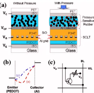
base electrode embedded in the organic layer. One of these vertical metal-base transistors, namely the space-charge-limited transistor共SCLT兲, shows promising performance.14,15 The SCLT is a vertical transistor with a grid electrode in-serted between emitter and collector to control the vertical current flow. The device structure of the SCLT is shown in Fig. 1共a兲. The grid contains random submicron openings formed by a nonlithographic method. The carriers are in-jected from the emitter into the semiconductor, passing through the openings on the metal grid and finally arriving at the collector. The voltages of grid and collector control the potential distribution between emitter and collector as shown
a兲Author to whom correspondence should be addressed. Electronic mail: [email protected].
FIG. 1. 共Color online兲 共a兲 The schematic device structure. The left part shows the device structure without pressure applied. The right part shows the device structure under pressure. Different graphite particles distributions in PDMS are also shown. The conductive paths break at the place indicated by red dashed circles.共b兲 The potential profile along the emitter—collector path through the opening when VCis fixed at a negative value. Curve共x兲 is a potential profile with energy barrier for hole. Curve 共y兲 is a potential profile without energy barrier for hole for a positive enough grid potential VG.共c兲 Circuit diagram of one active pressure sensor.
APPLIED PHYSICS LETTERS 95, 253306共2009兲
0003-6951/2009/95共25兲/253306/3/$25.00 95, 253306-1 © 2009 American Institute of Physics
This article is copyrighted as indicated in the article. Reuse of AIP content is subject to the terms at: http://scitation.aip.org/termsconditions. Downloaded to IP: 140.113.38.11 On: Wed, 30 Apr 2014 08:24:29
in Fig. 1共b兲. When high barrier forms between emitter and collector 关curve 共x兲兴, few carriers can arrive at the collector and this corresponds to the off state of the transistor. While low or no barrier forms关curve 共y兲兴, lots of carriers can arrive at the collector and this corresponds to the on state of the transistor.
In this letter, one pixel active pressure sensor operated with low voltage is demonstrated by vertically integrating SCLT with the pressure sensitive rubber as shown in Fig. 1共a兲. Circuit diagram of one active pressure sensor of an active matrix pressure sensor is shown in Fig. 1共c兲. The SCLT is represented by the symbol of bipolar junction tran-sistor. The pressure sensitive rubber is a composite contain-ing poly共dimethylsiloxane兲 共PDMS兲 and graphite particles, and it functions as a variable resistor. Integration between SCLT and pressure sensitive rubber is easy since both of them are in sandwich structures. Drilling process needed in previous work is avoided.6,7 The resistance of the pressure sensitive rubber changes when subjecting to a pressure and can be read out by the SCLT for pressure monitoring. The operation voltage of the integrated pressure sensor is as low as 4 V and the output current density is around 5 mA/cm2.
Furthermore, the response time of the pressure sensitive rub-ber to the pressure is as short as 22 ms. Such a fast response time makes the device suitable for serving as a component of active matrix pressure sensor array.
Since graphite particle is more incompressible compared with rubber, the response of the pressure sensitive rubber to the pressure mainly results from the deformation of the PDMS.17As the pressure is applied on the pressure sensitive rubber, the distribution of graphite particles in the PDMS changes as PDMS deforms. In this work, graphite particles are blended with PDMS in proper weight ratio to make graphite particles already constitute conductive paths in the rubber as shown in the left part of Fig.1共a兲. The application of external pressure extrudes graphite particles out of the conductive paths and increases the resistance of the pressure sensitive rubber as indicated in the red dashed circles in the right part of Fig.1共a兲. Without pressure, the pressure sensi-tive rubber shows the resistance comparable to the on state resistance of SCLT in the order of 104 ohm. While pressure
is applied on the pressure sensitive rubber, the pressure-dependent resistance falls in the range from on state resis-tance of SCLT to the off state resisresis-tance of SCLT.
The pressure sensor is fabricated by integrating the SCLT with the pressure sensitive rubber. After cleaning the substrate, a layer of 400 Å poly共3,4-ethylenedioxythiophene兲 doped with polystyrene sulfonated acid共PEDOT:PSS兲 is spin coated on ITO and annealed at 200 ° C for 10 min. After poly共3-hexylthiophene兲 共P3HT兲 is spin coated and annealed at 200 ° C for 10 min, the P3HT film is spin rinsed with xylene. The 2000 Å polystyrene spheres are absorbed on the P3HT surface as evaporation mask by submerging the sub-strate in a polystyrene spheres ethanol solution for 40 s. The substrate is then dipped in a boiling isopropanol solution for 10 s and blown dry in a nitrogen flow. After depositing 150 Å Al and 500 Å SiO as grid electrode and insulating layer, the spheres are removed by an adhesive tape. Another layer of 800 Å P3HT is then spin coated from xylene, following the deposition of 400 Å Al collector to complete the fabrica-tion procedures of the transistor. The transistor active area is 1 mm2. The pressure sensitive rubber is then prepared on top
of the transistor. The pressure sensing rubber is a blend of
PDMS and graphite particle共Sigma Aldrich兲 in weight ratio of 3.5:1. The diameter of the graphite powder is smaller than 20 m. The blend is then poured into a mold placed on the sample. The thickness of the pressure sensitive rubber is around 2 mm. After placing a sheet of ITO coated polyeth-ylene terepthalate共PET兲 flexible substrate on top of the pres-sure sensing rubber, whole device is annealed at 100 ° C for 10 min to cure PDMS and complete the device fabrication procedure.
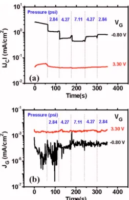
The electric characteristics of the pressure sensor with-out applying pressure are shown in Fig. 2. Voltages applied on ITO emitter, Al grid, Al collector, and ITO electrode on PET flexible substrate are represented by VE, VG, VCF, and
VC. The PEDOT:PSS covered ITO emitter is commonly grounded and hence VE is zero. VCFis floating and its value is determined by the voltage drop across the pressure sensi-tive rubber. While no pressure is applied on the device, the resistance of the pressure sensitive rubber is low and hence VCFis almost equals to the VC. Figure2共a兲demonstrates an apparent modulation of output current from the ITO elec-trode on PET 共兩JC兩兲 by VG from ⫺0.8 to 2.1 V while no pressure is applied. When VCis⫺4 V and VGis⫺0.8 V, the transistor output current density is 5.02 mA/cm2. The on/off
ratio 132 is obtained by dividing JC共VG= −0.8 V兲 by
JC共VG= 2.1 V兲 while VC is⫺3.12 V. Figure 2共b兲 shows the leakage current density JGof Al grid as a function of VC. JG keeps low under various biasing voltages. As VCis⫺4 V, the current gain 兩JC兩/JGis 6756.
While different pressure is applied on the device, ent amount of conductive paths break which result in differ-ent resistance value. Figure 3共a兲shows the response of兩JC兩 under various pressures. The pressure is created by placing weight on the device. When VGis⫺0.8 V, the transistor is in the on state, 兩JC兩 is decreased by applying 2.84 psi on the device. 兩JC兩 keeps at the same value until the pressure is changed. While increasing the pressure, 兩JC兩 decreases once FIG. 2.共Color online兲 共a兲 兩JC兩 and 共b兲 JGas a function of VCat various grid voltages of the pressure sensor with 2000 Å opening on Al grid.
253306-2 Chao et al. Appl. Phys. Lett. 95, 253306共2009兲
This article is copyrighted as indicated in the article. Reuse of AIP content is subject to the terms at: http://scitation.aip.org/termsconditions. Downloaded to IP: 140.113.38.11 On: Wed, 30 Apr 2014 08:24:29
again. As the pressure is decreased from 7.11 to 4.27 psi,兩JC兩 recovers almost to its original value under the pressure of 4.27 psi. On the other hand, when VGis 3.3 V, the transistor is in the off state,兩JC兩 keeps at the same value without chang-ing with pressure. At this time, the resistance of the SCLT is larger than the pressure sensitive rubber. The voltage differ-ence on the pressure sensitive rubber is small and the re-sponse on pressure cannot be resolved from兩JC兩. Figure3共b兲 shows that JG also keeps at the same value under various pressure. These results suggest that the integration between SCLT and pressure sensitive rubber is an excellent candidate for pressure sensor.
Furthermore, the response time of the pressure sensitive rubber is also investigated. The response time is recorded with the circuit as shown in the inset of Fig.4. The pressure sensitive rubber is connected in series with a 10 k⍀ resistor
in order to probe the variation in the resistance of the pres-sure sensitive rubber. The response time is defined as the time required for the voltage drop across the resistor de-creases to half of its original value. Before applying pressure, the voltage drop across the resistor is about 1.25 V. When we touch the pressure sensitive rubber carefully by hand, the voltage drops to the value almost zero within 50 ms. This changing from low to high resistance is matching to the re-sult shown in Fig. 3. It takes about 22 ms for the voltage across the resistor drops to 0.625 V. The actual response time of the pressure sensitive rubber may be faster than 22 ms since the deformation of the soft tissue on hand also takes place. Such a short response time is suitable for a high sen-sitive pressure sensor.
In summary, the pressure sensitive rubber is vertically integrated with SCLT to demonstrate one pixel active pres-sure sensor. The operation voltage of this prespres-sure sensor is as low as 4 V, and the response time is as short as 22 ms. Since the pressure sensitive rubber is also in the sandwich structure, the integration between SCLT and pressure sensi-tive rubber is easy. The integration is also applicable for any other devices with sandwich structure such as photodiode and light-emitting diode. Such device concept has the poten-tial advantages of easy large-area solution process, low volt-age, and being lithography-free.
This work is supported by the National Science Council of Taiwan under Contract No. NSC98-2628-M-009-001.
1R. H. Reuss, B. R. Chalamala, A. Moussessian, M. G. Kane, A. Kumar, D. C. Zhang, J. A. Rogers, M. Hatalis, D. Temple, G. Moddel, B. J. Eliasson, M. J. Estes, J. Kunze, E. S. Handy, E. S. Harmon, D. B. Salzman, J. M. Woodall, M. A. Alam, J. Y. Murthy, S. C. Jacobsen, M. Olivier, D. Markus, P. M. Campbell, and E. Snow,Proc. IEEE 93, 1239共2005兲. 2E. C. Chen, J. H. Ju, C. M. Yang, S. F. Horng, S. R. Tseng, H. F. Meng,
and C. F. Shu,Appl. Phys. Lett. 93, 063304共2008兲.
3I. Manunza, A. Sulis, and A. Bonfiglio, Appl. Phys. Lett. 89, 143502 共2006兲.
4S. Jung, T. Ji, and V. K. Varadan,Appl. Phys. Lett. 90, 062105共2007兲. 5V. J. Lumelsky, M. S. Shur, and S. Wagner,IEEE Sens. J. 1, 41共2001兲. 6Y. Noguchi, T. Sekitani, and T. Someya,Appl. Phys. Lett. 89, 253507
共2006兲.
7T. Someya, T. Sekitani, S. Iba, Y. Kato, H. Kawaguchi, and T. Sakurai, Proc. Natl. Acad. Sci. U.S.A. 101, 9966共2004兲.
8Y. Yang and A. J. Heeger,Nature共London兲 372, 344共1994兲.
9Y. C. Chao, S. L. Yang, H. F. Meng, and S. F. Horng,Appl. Phys. Lett.87, 253508共2005兲.
10Y. C. Chao, M. H. Xie, M. Z. Dai, H. F. Meng, S. F. Horng, and C. S. Hsu, Appl. Phys. Lett. 92, 093310共2008兲.
11K. Kudo, D. X. Wang, M. Iizuka, S. Kuniyoshi, and K. Tanaka,Synth.
Met. 111, 11共2000兲.
12Y. Watanabe and K. Kudo,Appl. Phys. Lett. 87, 223505共2005兲. 13K. Fujimoto, T. Hiroi, K. Kudo, and M. Nakamura,Adv. Mater. 19, 525
共2007兲.
14Y. C. Chao, H. F. Meng, and S. F. Horng,Appl. Phys. Lett. 88, 223510 共2006兲.
15Y. C. Chao, H. F. Meng, S. F. Horng, and C. S. Hsu,Org. Electron.9, 310 共2008兲.
16J. Huang, M. Yi, D. Ma, and I. A. Hümmelgen,Appl. Phys. Lett. 92, 232111共2008兲.
17T. Ding, L. Wang, and P. Wang,J. Polym. Sci., Part B: Polym. Phys. 45, 2700共2007兲.
FIG. 3. 共Color online兲 The response of 共a兲 兩JC兩 and 共b兲 JGunder various pressure. VGis⫺0.8 and 3.3 V. VCis biased at⫺4 V.
0 100 200 300 400 -0.5 0.0 0.5 1.0 1.5 V o ltage (V) Time (ms)
FIG. 4. The response of the pressure sensitive rubber. The inset shows the measuring circuit.
253306-3 Chao et al. Appl. Phys. Lett. 95, 253306共2009兲
This article is copyrighted as indicated in the article. Reuse of AIP content is subject to the terms at: http://scitation.aip.org/termsconditions. Downloaded to IP: 140.113.38.11 On: Wed, 30 Apr 2014 08:24:29