Reduced temperature-quenching of photoluminescence from indium nitride nanotips
grown by metalorganic chemical vapor deposition
Shih-Chen Shi, Chia-Fu Chen, Geng-Ming Hsu, Jih-Shang Hwang, Surojit Chattopadhyay, Zon-Huang Lan,
Kuei-Hsien Chen, and Li-Chyong Chen
Citation: Applied Physics Letters 87, 203103 (2005); doi: 10.1063/1.2128484 View online: http://dx.doi.org/10.1063/1.2128484
View Table of Contents: http://scitation.aip.org/content/aip/journal/apl/87/20?ver=pdfcov
Published by the AIP Publishing
Articles you may be interested in
High optical quality polycrystalline indium phosphide grown on metal substrates by metalorganic chemical vapor deposition
J. Appl. Phys. 111, 123112 (2012); 10.1063/1.4730442
Photoluminescence properties of ZnO nanoneedles grown by metal organic chemical vapor deposition
J. Appl. Phys. 104, 064311 (2008); 10.1063/1.2980335
Studies of InGaN GaN multiquantum-well green-light-emitting diodes grown by metalorganic chemical vapor deposition
Appl. Phys. Lett. 85, 401 (2004); 10.1063/1.1773371
InGaN self-assembled quantum dots grown by metalorganic chemical-vapor deposition with indium as the antisurfactant
Appl. Phys. Lett. 80, 485 (2002); 10.1063/1.1433163
Effects of growth interruption on the optical and the structural properties of InGaN/GaN quantum wells grown by metalorganic chemical vapor deposition
J. Appl. Phys. 90, 5642 (2001); 10.1063/1.1410320
This article is copyrighted as indicated in the article. Reuse of AIP content is subject to the terms at: http://scitation.aip.org/termsconditions. Downloaded to IP: 140.113.38.11 On: Thu, 01 May 2014 02:45:03
Reduced temperature-quenching of photoluminescence from indium nitride
nanotips grown by metalorganic chemical vapor deposition
Shih-Chen Shi and Chia-Fu Chen
Department of Materials Science and Engineering, National Chiao Tung University, Hsinchu 300, Taiwan, Republic of China
Geng-Ming Hsu and Jih-Shang Hwang
Institute of Optoelectronic Sciences, National Taiwan Ocean University, Keelung 202, Taiwan, Republic of China
Surojit Chattopadhyay, Zon-Huang Lan, and Kuei-Hsien Chen
Institute of Atomic and Molecular Sciences, Academia Sinica, Taipei 106, Taiwan, Republic of China
Li-Chyong Chena兲
Center for Condensed Matter Sciences, National Taiwan University, Taipei 106, Taiwan, Republic of China
共Received 24 June 2005; accepted 14 September 2005; published online 8 November 2005兲 We report metalorganic chemical vapor deposition of indium nitride共InN兲 nanotips with apex angles of 10° and length and base diameter of around 1m and 200 nm, respectively. The structure of the hexagonal InN nanotips growing along 关002兴 was studied by electron microscopy and x-ray diffraction, and the optical properties were studied using temperature-dependent photoluminescence 共PL兲 measurements. A narrow emission peak with a 18 meV full width at half maximum positioned at 0.77 eV was obtained with no visible emission. A PL quenching of only 14% was observed with a temperature scan of 15–320 K. © 2005 American Institute of Physics.关DOI:10.1063/1.2128484兴
Indiun nitride 共InN兲 is a key element in InGaN-based light emitting diodes 共LEDs兲1,2 and also for high speed electronics3 owing to its low electronic effective mass and high mobility.1,2 However, the recent controversy about the fundamental band gap of InN has generated renewed interest in the material. The initial estimation at near 1.9 eV4 has been challenged by Davydov et al.5suggesting it to be near 0.7 eV evident from photoluminescence共PL兲 measurements and absorption spectroscopy. Several other reports have con-firmed such finding6,7and the apparent band gap near 1.9 eV was generally ascribed to the contribution from indium oxide related phase in the sample.5 Other possible origins for the visible emission are the quantum size effect,8 the Burstein– Moss shift9 and nitrogen excesses in InN.10 InN thin films have been prepared by several routes including metalorganic chemical vapor deposition共MOCVD兲, molecular beam epi-taxy, chemical beam epiepi-taxy, and vapor phase epitaxy.11The window for the growth temperature is narrow because of nitrogen dissociation from InN around 550 °C. Reports on nanostructured InN are scarce. InN nanoparticles12 and nanowires13–15have been reported by the wet chemical syn-thesis and vapor-liquid-solid 共VLS兲 routes. Recently, there has been a report on InN nanotube synthesis by a controlled carbonitridation reaction.16 The scarcity of reports suggests that there are challenges involved in growing good quality InN nanostructures. This letter describes the MOCVD of single crystalline InN ‘nanotips’共InNNTs兲 and evaluates the structural quality and the optical behavior of the material.
InNNTs were grown by the resistively heated MOCVD on gold共2 nm兲 coated quartz substrates held at 550°C and 50 Torr pressure for 90 min.17Epi-grade tri-methyl indium 共EP-ICHEM, UK兲 and high purity 共99.999%兲 ammonia were
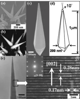
used as growth precursors and high purity nitrogen was used as a carrier gas. Figure 1 shows a series of InNNT images taken collectively by high resolution scanning electron mi-croscopy共JEOL 5700F HRSEM兲 关Figs. 1共a兲, 1共b兲, and 1共c兲兴 and high resolution transmission electron microscopy 关HRTEM/ JEOL JEM 4000 EX兲 关Figs. 1共e兲 and 1共f兲兴. The sharply faceted, hexagonal InNNTs growing along关002兴 are shown to carry a catalyst共Au in this case兲 at its apex which is less than 10 nm in diameter 关1共b兲兴 and having an apex angle of⬃10°. To our knowledge this is the first observation of solid InN nanotips, whereas that reported by Yin et al.16 was a tubular form of InN. The schematic of the individual
a兲Author to whom correspondence should be addressed; electronic mail:
FIG. 1.共a兲 SEM image and 共b兲 backscattered SEM image of InN nanotips; 共c兲 low magnification SEM image and 共d兲 schematic diagram of a single InN nanotip;共e兲 low magnification TEM image of a single nanotip and 共f兲 HR-TEM of the InN nanotip area marked in共e兲; inset showing the selected area diffraction pattern of h-InN nanotip.
APPLIED PHYSICS LETTERS 87, 203103共2005兲
0003-6951/2005/87共20兲/203103/3/$22.50 87, 203103-1 © 2005 American Institute of Physics This article is copyrighted as indicated in the article. Reuse of AIP content is subject to the terms at: http://scitation.aip.org/termsconditions. Downloaded to IP:
InNNT关Fig. 1共d兲兴 shows its representative dimensions. The selected area electron diffraction共SAED兲 of the InNNT 关in-set, Fig. 1共f兲兴 also speaks of the good quality single crystal-line hexagonal phase. The presence of polycrystalcrystal-line InN grains, which can complicate the interpretations of the PL data presented later, can be ruled out from the observed SAED pattern 关inset, Fig. 1共f兲兴 and the HRTEM images 关Figs. 1共e兲 and 1共f兲兴.
The composition of the InNNTs has been established from electron energy loss spectroscopy共EELS兲. The nitrogen K edge and the In M4,5edges, along with the fine structures, 18
were clearly seen in EELS data 关Fig. 2共a兲兴. Further infor-mation on the structural quality of the InNNTs can be ob-tained from the x-ray diffraction 共XRD兲 共Rigaku DMAX/C x-ray diffractometer兲. The XRD spectrum 关Fig. 2共b兲兴 shows signature peaks of the hexagonal InN phases共Joint Commit-tee for Powder Diffraction Standards, card No. 02-1450兲.
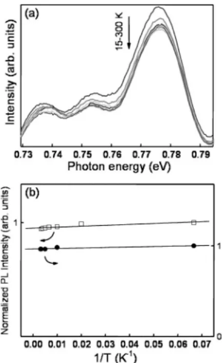
The infrared 共IR兲 range PL was taken from a conven-tional PL setup equipped with an InGaAs detector using Ar-gon 488 and 514 nm line for excitation. The PL spectra of the InNNTs measured with 488 nm laser and a 3 mm slit on the detector path are shown in Fig. 3共a兲. A sharp emission peak at 0.77 eV5,6 was observed with a linewidth full width at half maximum of 18 meV with no significant emission around the visible. A weak peak near 0.754 eV may be due to 20-meV-deep donor level in InN.19 The peak at⬃0.735 eV could not be assigned at the present. Temperature depen-dence of the IR-PL peak measured with an incident laser power of 100 mW shows less than 14% 共factor of 1.15兲 decrease in the emission intensity when the temperature was varied from 15 to 300 K关open squares, Fig. 3共b兲兴. The PL efficiency共兲 defined as the ratio of the radiative transition probability 共Pr兲 and the sum of radiative and nonradiative
transition probabilities, can be written as20
= Pr
关Pr+ A
Pnr+BPnr兴, 共1兲
whereAPnr, andBPnr, are transition probabilities for two non-radiative mechanisms in different temperature regimes. The temperature dependence of the nonradiative transition prob-abilities can be written as
X
Pnr= X exp
冉
− EXT
冊
共2兲with X = A, or B, where EAand EBare the thermal activation
energies for the two processes, and A and B are temperature independent prefactors. The temperature dependent effi-ciency can hence be written as
共T兲 = 1
冋
1 + A Pr exp冉
−EA T冊
+ B Pr exp冉
− EB T冊
册
. 共3兲Here, Pr is assumed to be independent of temperature.
As-suming the efficiency,, to be solely governing the PL in-tensity and that共15 K兲=100%, a high internal efficiency at room temperature can be estimated from Fig. 3. Indication about the magnitude of the activation energies共EA and EB兲
can be obtained from the Arrhenius plot of the normalized PL intensity as a function of inverse temperature关Fig. 3共b兲兴 and its linear fit according to Eq.共3兲. Generally, two distinct regions, one with a high activation near room temperatures and another with low activation at low temperatures, were obtained. Two features stand out from Fig. 3共b兲. First, is the extremely small value of the activation energy 共EA
⬍6 meV兲 at low temperatures that supports the assumption 共共15 K兲=100%兲 made earlier. Second, is the absence of the PL quenching near room temperature, which, when present, will give rise to the second region with a high ther-mal activation energy共EB兲. For multiple quantum wells, such
FIG. 2.共a兲 EELS result showing the N–K edge and the In M4,5-edge spectra
for the InN nanotips;共b兲 the x-ray diffraction spectrum of the InN nanotips showing the hexagonal signature.
FIG. 3.共a兲 The temperature dependent PL spectra of InN nanotips measured with 100 mW incident laser power and 3 mm slit width.共b兲 Two sets of Arrhenius plot of the normalized integrated photoluminescence intensity as a function of inverse temperature:共䊐兲 15–300 K, 488 nm laser, 3 mm slit width共䊏兲 15–320 K, 514 nm laser, 0.5 mm slit width.
203103-2 Shi et al. Appl. Phys. Lett. 87, 203103共2005兲
This article is copyrighted as indicated in the article. Reuse of AIP content is subject to the terms at: http://scitation.aip.org/termsconditions. Downloaded to IP: 140.113.38.11 On: Thu, 01 May 2014 02:45:03
as InGaP/ AlGaInP, the thermal activation energy EA
ac-counts for loss mechanism within the well, whereas EB
ac-counts for carrier emission outside the well followed by non-radiative recombination in the barriers.21 The small activation energy共EA兲 below room temperature can be
attrib-uted to excitonic binding energy with impurities. But Lam-bkin et al.20specified EA to be responsible for carriers
ther-malizing from localized regions of order induced band edge fluctuations in InGaP materials. In some cases the activation energy, EB, was attributed to nonradiative recombination in
the dislocations.22
The absence of the room temperature PL quenching was somewhat unusual and double checked with a 514 nm exci-tation and a 0.5 mm slit on the detector path. The narrowing of the slit width did reduce the overall intensity of the 0.77 eV line but the temperature dependence carried out from 15 to 320 K, in this case, showed a similar absence of quench-ing关filled circles, Fig. 3共b兲兴 and a small activation energy of 5.2 meV. In comparison, the GaAsSb/ GaAs quantum wells showed a marked PL quenching measured in the same PL instrumental setup.23Also InN films show a marked quench-ing in the vicinity of room temperature.24 The features of Fig. 3 taken together speak of a high internal quantum effi-ciency in the InN material. Nonradiative recombination in defects, such as dislocations, is minimal. The absence of PL quenching near room temperature clearly indicates a mini-mum thermal escape of carriers from any confining potential within the InNNTs. We have already ruled out polycrystal-line grains in the material that could account for nonradiative recombinations. Although we cannot ignore the presence of surface states in nanomaterials, clearly these surface states are not populated even at room temperature, because of a strong electron-hole coupling in the bulk. The surface states can again be passivated by a wide bandgap InO layer, on these InNNTs, blocking the thermal escape routes of the car-riers due to large energy requirements. Even after the report of the IR band gap of InN there are reports that still support the visible 1.9 eV band gap of InN.16Many reports indicated that the visible band gap may be due to InO in the material.25 The absence of the visible PL in our case can be due to 共i兲 absence of significant proportion of InN nanocrystals 共⬍5 nm兲 that can shift the IR peak into the visible with the assumption of an ultrasmall electron effective mass 共0.042 m0兲,8 共ii兲 low carrier concentration in the crystal to
minimize any Burstein–Moss shift9 which has the ability to shift the band gap from 0.7 to 1.7 eV,26 and共iii兲 absence of excess nitrogen in InN.10 High-quality stoichiometric InN film with carrier concentration of high 1017cm−3and
mobil-ity in excess of 1000 cm2V−1s−1 was reported to have PL
emissions at 0.70 eV.27The other possibility of optical tran-sitions between interface states of metallic In clusters in the InN matrix28 can be effectively ruled out since we did not observe the In clusters in our TEM measurements. Moreover, if the In clusters were to dominate the PL measurements, its density must be high enough to be observable under TEM and XRD which is not the case in the present study as well as that reported.27
In summary, we have demonstrated the growth of solid indium nitride nanotips, with apex angles of 10 ° and lengths of 1m, by metalorganic chemical vapor deposition at tem-peratures of 550 °C. The VLS grown InN nanotips were found to be hexagonal with a 关002兴 axial growth direction.
High resolution TEM demonstrated the nearly defect free structure of the nanotips corroborated by the weak quenching 共⬍14%兲 of the 0.76 eV photoluminescence peak intensity over a 285 K temperature scan.
Support from Academia Sinica, NSC and MOE, Taiwan, and the U.S. Air Force of Scientific Research/Asian Office of Aerospace Research and Development is gratefully acknowl-edged. The authors thank Professor Y. F. Chen, National Tai-wan University, for useful discussion and the use of the IR-PL setup.
1S. Chichibu, T. Azuhata, T. Sota, and S. Nakamura, Appl. Phys. Lett. 69,
4188共1996兲.
2K. P. O’Donell, R. W. Martin, and P. G. Middleton, Phys. Rev. Lett. 82,
237共1999兲.
3B. E. Foutz, S. K. O’Leary, M. S. Shur, and L. F. Eastman, J. Appl. Phys.
85, 7727共1999兲.
4T. L. Tansley and C. P. Foley, J. Appl. Phys. 59, 3241共1986兲.
5V. Y. Davydov, A. A. Klochikhin, R. P. Seisyan, V. V. Emtsev, S. V.
Ivanov, F. Bechstedt, J. Furthmuller, H. Harima, A. V. Mudryi, J. Ader-hold, O. Semchinova, and J. Grual, Phys. Status Solidi B 229, R1共2002兲.
6J. Wu, W. Walukiewicz, K. M. Yu, J. W. Ager III, E. E. Haller, H. Lu, W.
J. Schaff, Y. Saito, and Y. Nanishi, Appl. Phys. Lett. 80, 3967共2002兲.
7T. Matsuoka, H. Okamoto, M. Nakao, H. Harima, and E. Kurimoto, Appl.
Phys. Lett. 81, 1246共2002兲.
8B. R. Nag, Phys. Status Solidi B 237, R2共2003兲.
9J. Wu, W. Walukiewicz, W. Shan, K. M. Yu, J. W. Ager III, E. E. Haller,
H. Lu, and W. J. Schaff, Phys. Rev. B 66, 201403共2002兲.
10T. V. Shubina, S. V. Ivanov, V. N. Jmerik, M. M. Glazov, A. P. Kalvarskii,
M. G. Tkachman, A. Vasson, J. Leymarie, A. Kavokin, H. Amano, I. Akasaki, K. S. A. Butcher, Q. Guo, B. Monemar, and P. S. Kop’ev, Phys. Status Solidi A 202, 377共2005兲.
11A. G. Bhuiyan, A. Hashimoto, and A. Yamamoto, J. Appl. Phys. 94, 2779
共2003兲.
12S. D. Dingman, N. P. Rath, P. D. Markowitz, P. C. Gibbons, and W. E.
Buhro, Angew. Chem., Int. Ed. 39, 1470共2000兲.
13C. H. Liang, L. C. Chen, J. S. Hwang, K. H. Chen, Y. T. Hung, and Y. F.
Chen, Appl. Phys. Lett. 81, 22共2002兲.
14K. Sardar, F. L. Deepak, A. Govindaraj, M. M. Seikh, and C. N. R. Rao,
Small 1, 91共2005兲.
15J. Zhang, B. L. Xu, F. H. Jiang, Y. D. Yang, and J. P. Li, Phys. Lett. A 337,
121共2005兲.
16L. W. Yin, Y. Bando, D. Golberg, and M. S. Li, Adv. Mater.共Weinheim,
Ger.兲 16, 1833 共2004兲.
17J. S. Hwang, C. H. Lee, F. H. Yang, K. H. Chen, L. G. Hwa, Y. J. Yang,
and L. C. Chen, Mater. Chem. Phys. 72, 290共2001兲.
18K. A. Mkhoyan, J. Silcox, E. S. Alldredge, N. W. Ashcroft, H. Lu, W. J.
Schaff, and L. F. Eastman, Appl. Phys. Lett. 82, 1407共2003兲.
19S. Z. Wang, S. F. Yoon, Y. X. Xia, and S. W. Xie, J. Appl. Phys. 95, 7998
共2004兲.
20J. D. Lambkin, L. Considine, S. Walsh, G. M. O’Connor, C. J. McDonagh,
and T. J. Glynn, Appl. Phys. Lett. 65, 73共1994兲.
21E. M. Daly, T. J. Glynn, J. D. Lambkin, L. Considine, and S. Walsh, Phys.
Rev. B 52, 4696共1995兲.
22A. Hangleiter, Phys. Rev. B 48, 9146共1993兲.
23Y. S. Chiu, M. H. Ya, W. S. Su, and Y. F. Chen, J. Appl. Phys. 92, 5810
共2002兲.
24R. Intartaglia, B. Maleyre, S. Ruffenach, O. Briot, T. Taliercio, and B. Gil,
Appl. Phys. Lett. 86, 142104共2005兲.
25M. Yoshimoto, H. Yamamoto, W. Huang, H. Harima, J. Saraie, A.
Chaya-hara, and Y. Horino, Appl. Phys. Lett. 83, 3480共2003兲.
26J. Wu, W. Walukiewicz, S. X. Li, R. Armitage, J. C. Ho, E. R. Weber,
E. E. Haller, H. Lu, W. J. Schaff, A. Barcz, and R. Jakiela, Appl. Phys. Lett. 84, 2805共2004兲.
27K. M. Yu, Z. Liliental-Weber, W. Walukiewicz, W. Shan, J. W. Ager III,
S. X. Li, R. E. Jones, E. E. Haller, H. Lu, and W. J. Schaff, Appl. Phys. Lett. 86, 071910共2005兲.
28T. V. Shubina, S. V. Ivanov, V. N. Jmerik, D. D. Solnyshkov, V. A.
Vek-shin, P. S. Kop’ev, A. Vasson, J. Leymarie, A. Kavokin, H. Amano, K. Shimono, A. Kasic, and B. Monemar, Phys. Rev. Lett. 92, 117407 共2004兲.
203103-3 Shi et al. Appl. Phys. Lett. 87, 203103共2005兲
This article is copyrighted as indicated in the article. Reuse of AIP content is subject to the terms at: http://scitation.aip.org/termsconditions. Downloaded to IP: 140.113.38.11 On: Thu, 01 May 2014 02:45:03