行政院國家科學委員會專題研究計畫 成果報告
子計畫二:各種型態之奈米碳基材料開發及場發射元件之製
作(3/3)
計畫類別: 整合型計畫 計畫編號: NSC93-2216-E-009-007- 執行期間: 93 年 08 月 01 日至 94 年 07 月 31 日 執行單位: 國立交通大學材料科學與工程學系(所) 計畫主持人: 陳家富 計畫參與人員: 徐振航,劉家駿,陳瑤真,洪淙琦 報告類型: 完整報告 處理方式: 本計畫可公開查詢中 華 民 國 94 年 12 月 7 日
行政院國家科學委員會專題研究計畫期中報告
光資訊關鍵性材料製程與性質研究-子計畫二:各種型態之奈米
碳基材料開發及場發射元件之製作
執行期限:91 年 8 月 1 日至 94 年 7 月 31 日 主持人:陳家富 國立交通大學 材料科學與工程學系 國立交通大學 材料科學與工程學系 AbstractWith the development of nanotechnology, nanostructures structures that are defined as having at least one dimension between 1 and 100 nm have received steadily growing interest as a result of their peculiar and fascinating properties, and applications superior to their bulk counterparts. Many applications are predicted to involve with nanotechnology including optics, electronics, catalyst, ceramics, and storage media, etc. The most pertinent example is micro - electronics, which “smaller” means greater performance ever since the invention of integrate circuits: more components per chip, faster operation, lower cost, and less power consumption.
Field emission from nano-sized material is one of the most important applications for the nanotechnology. The basic requirement of a nano emitter must have a high aspect ratio that field emission will take place. Among such an application, a revolution of the display technology come the field emission display. Compare with TFT-LCD flat panel display, field emission display has much more advantages such as high brightness, thin in dimension, wide view angle, low power consumption and a wide operating temperature. The mention advantages above make the field emission display a candidate for the new generation of the display technology.
Though the field emission technology has been developed over decades, a satisfied product has not yet been demonstrated. The key resolution of the current field emission display difficulties is the field emission efficiency and durability of the emitters. So far, carbon nanotubes have been extensively studied and tested for applications. It is not until now that precisely controlling the dimension and distribution of carbon nanotubes still a
challenging issue. There’s still many materials which prohibit better performances than carbon nanotubes do.
In this project, various kinds of deposition methods are involved to synthesized nano-size materials. After the synthesis, instruments are incorporated to analysis and measure the character of the material. At the final stage, the material with desirable performance will be fabricated in to the device to achieve the practical applications.
Result and discussion
(a) Sysnthesis of carbon nanotips and fabrication of triode structure
(b) Growth of Chromium carbide capped - carbon nanotips
(c) Modification of Si Nano Emitters by Diamond - clad Process
(d) Growth and purification of carbon nanotubes
(a)Sysnthesis of carbon nanotips and fabrication of triode structure
It is considered that the carbon active species in the plasma are accelerated to the substrate by the negative bias to form sp2 and non-crystalline clusters in the nucleation period. Some clusters are then transformed into sp3 clusters through the collision of carbon species in the growth period. Meanwhile, the accelerated active hydrogen radicals will remove the other sp2 clusters with lower active energy. In this situation, the competition between etching and deposition is repeated. Nevertheless, biasing the samples can cause their rate of deposition to exceed the rate of etching. Many reports have presented the method to enhance the nucleation density of diamond by applying negative bias. This study focuses mainly on determining the optimum negative bias to synthesize the carbon nanotips.
Figure 1
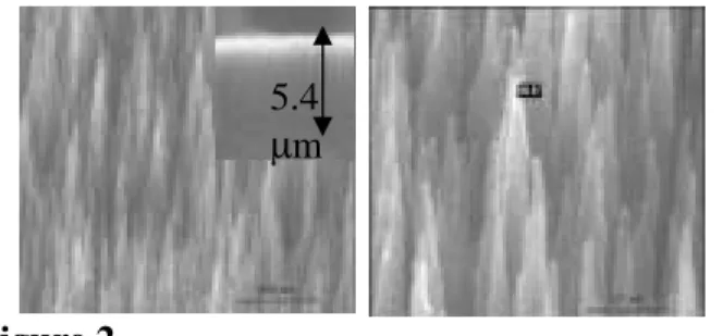
Figures 1 ~ 3 present the scanning electron microscope (SEM) pictures of carbon nanotips grown under various biases and substrates. The photograph on the right of each figure is the
enlarged image. Fig.1 (a) displays that there only a low density of tiny nanotips can be grown under -80V. This also implies that samples grown under a bias less negative than –80V cause little carbon materials on the Pt films. Increasing the bias to –120V, it generates the high-density carbon nanotips.
Fig. 2 shows these well-aligned carbon nanotips grown upward to 5.4 µm length and 64 nm in diameter under -120V. Sharper nanotips have a higher-aspect-ratio, indicating good characteristics for field emission. Fig. 1(b, however indicates that tips will grow to a sub-micrometer diameter under a higher bias (more negative than –120V), revealing that bias can enhance the growth of carbon nanotips on Pt films. Hence, the optimal bias for growing carbon nanotips on Pt films is –120V.
Figure 2
Figure 3 also shows good results of carbon nanotips grown on Si under –120V, but the deposition time is shorter than those grown on Pt films. This is due to the fact that it is easier to form carbon materials on Si than on Pt .
Figure 3
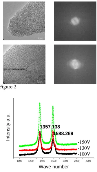
Figure 4 (a) displays the TEM images of an end section of an individual nanotip grown under –120V. Unlike hollow carbon nanotubes, carbon nanotips are solid. The main feature of note is the tip’s somewhat irregular shape, with one primary protrusion. The diffraction pattern (DP) indicates that the end section is graphite. Moreover, Fig. 4 (b) displays the lateral section of the same tip, showing well-organized microcrystalline graphite section. The DP of Fig. 4 (b) also confirms the existence of
5.4 µm
well-organized microcrystalline graphite, proveing that the carbon nanotips are made of graphite.
Figure 4
Figure5 exhibits the Raman spectra of carbon nanotips grown under various bias and substrates. All of them have two sharp peaks located on about 1345 cm-1 and 1580 cm-1, respectively. The first-order Raman spectrum of aligned carbon nanotips shows strong sharp
peaks at 1581 cm-1 (G line), which is the
high-frequency E2g first-order mode and 1350
cm-1 (roughly corresponding to the D-line
associated with disorder-allowed zone-edge modes of graphite). The peaks imply that the nanotips are characteristic of microcrystalline graphite. The relative intensities of the two peaks depend on the type of graphitic material. Normally, the intensity of the 1350cm-1 peak increases (i) with an increase in the amount of unorganized carbon in the samples and (ii) with a decrease in the graphite crystal size .
The most conspicuous feature of carbon nanotips (grown under –120V) is that their Raman spectra show an additional weak peak at about 1618 cm-1 (D’ line). The origin of the D and D’ lines in other forms of carbon materials has been explained as disorder-induced features, caused by the finite particle size effect or lattice distortion . Besides, a sample grown under –120 V with a narrow bandwidth of the G-line and the D-line has well-organized carbon. The previous TEM image clearly displays the existence of well-organized graphite in the sample. 1000 1200 1400 1600 1800 2000 -120V on Si -120V on Pt -80V on Pt -150V on Pt In te ns ity ( a.u) Wave number Figure 5
The field emission tests are performed on a diode structure, in which the carbon nanotips are separated from the anode, indium-tin-oxide glass, using 500 µm glass as spacers. The voltage-current ( I-V ) properties are measured and analyzed through the Fowler-Nordheim (FN) model, viz the ln ( I/V2 ) VS. 1/V plot. Fig. 6
characterizes carbon nanotips grown under –120V on Si and Pt. The current densities at 2.2V/ µm of nanotips under –120V grown on Si and Pt are 761 and 617 µA/cm2
, respectively. The threshold voltage ( VT ) is defined as the
intersection of the slope of F-N plots with abscissa. According to the F-N analysis, the emission behavior of the sample grown on the
Figure 6
Pt films is better than that grown on Si. (lower turn-on field = 1.5 V/µm). It is attributed
0.0 0.5 1.0 1.5 2.0 2.5 0 100 200 300 400 500 600 700 800 Curre nt de ns it y (µ A /c m 2) Electric field ( V/µ m) 0 2 4 6 8 10 -12 -10 -8 -6 Ln ( I/V 2 ) 1000/V 0.0 0 .5 1.0 1 .5 2 .0 2.5 0 10 0 20 0 30 0 40 0 50 0 60 0 70 0 80 0 C u rr ent de nsity (µ A /cm 2 ) E lectric field ( V /µ m ) 0 2 4 6 8 10 -1 2 -1 0 -8 -6 Ln ( I/ V 2 ) 10 00 /V
to the presence of Pt layers, which provide a good conduction path for electrons to transport from the cathode to the emission sites.
Vertically well-aligned, high-aspect-ratio carbon nanotips have been directly grown upward on the gated device structure with 4 µm gate aperture. The nanotips rapidly nucleate and grow without any catalyst. In addition, selected area deposition of nanotips is achieved by using a Pt layer as inhibitor in the bias-assisted microwave plasma chemical vapor deposition. The field emission current of nanotips on the gated structure is 154 µA (at a gate-to -cathode voltage of Vgc= 50V). This results from the
following reasons. (I) short gate-tips spacing, (II) small gate aperture, and (III) the high-aspect-ratio of nanotips.
Figure 1
A Pt-gated device structure with 50 x 50 circles was initially fabricated by semiconductor process technology. Starting substrates were mirror-polish n-type, (100) oriented wafers. The width and the depth of each circle were 4 µm and 7000Å, respectively. After the gated device structure was generated, specimens were put in the bias-assisted microwave plasma chemical vapor deposition system to deposit carbon nanotips. Reactive gaseous mixture of CH4-CO2
was used in deposition. The flow rates of
CH4/CO2 and the deposition time remained
constant at 30/30 sccm and 15 minutes, respectively. During deposition, the Si substrate
was subjected to a negative bias voltage.
Figure 1 shows SEM photographs of carbon nanotips grown under different biases. Each picture is only one of the 50 x 50 circles on the device. On the right side of every picture is an enlarged image. The SEM images indicate that carbon nanotips can be uniformly grown only inside the Pt-gated device structure in the absence of amorphous carbon (a-C) on the Pt-gated surface. The selective area deposition of nanotips is attributed to the following two reasons. One is that carbon materials are more easily grown on silicon than on the Pt-gated layer because Pt is a highly chemically inert material that does not nucleate carbon materials on an unscratched Pt surface. The other is that electrical field is concentrated on the silicon substrate surface because the n-type silicon conducts electrons, but electrons can not pass through silicon dioxide (dielectric layer) within a Pt-gated layer. Consequently, the local deposition biased effects are all within the silicon substrate. However, increasing the deposition time causes some a-C to form on the Pt-gated surface.
Figures 1(a) ~ (c) reveal that applying a bias can enhance the growth of carbon nanotips in CH4/CO2 gas mixture. Thus, the higher bias
drastically enhances the growth of carbon nanotips. The bias-assisted effect is also valid for the hydrocarbon diluted in hydrogen. However, samples grown under a bias more negative than -130V cause the height of the tips to exceed that of the Pt-gate. In this situation, the gated device structure becomes a diode structure. By contrast, a bias less negative than -130V only leads to tiny tips inside the hole. In addition, all the tips grow upward under biased conditions. The tip angle of the nanotips decreases as the bias increases. In other words, a higher bias generates higher density, sharper and
higher-aspect-ratio nanotips. CH4/CO2 can
promote the growth rate over that with conventional gas mixtures (hydrocarbons diluted in hydrogen, for example, CH4/H2)
because of the high carbon concentration in the CH4/CO2 gas mixture.
Figure 2 (a) displays the TEM images of an end section of an individual nanotip. The main feature of note is the tip’s somewhat irregular shape, with one primary protrusion. The Fourier filtering transformation (FFT) indicates that the end section is amorphous carbon. Moreover,
Fig. 2 (b) displays the lateral section of the same tip. It shows microcrystalline graphite on the lateral section. The FFT of Fig. 2 (b) also proves the existence of the microcrystalline graphite.
Figure 2
Figure 3
Figure 3 presents Raman spectra of tips grown under various applied biases. The spectra do not obviously differ. All of them have two sharp peaks located on about 1355 cm-1 and 1582 cm-1, respectively. The peaks imply that the nanotips are characteristic of microcrystalline graphite. The Raman spectra of amorphous carbon can be decomposed into two
features located approximately at 1550cm-1
(corresponding to the G-line associated with the
optically allowed E2g zone center mode of
crystalline graphite) and 1350 cm-1 (roughly corresponding to the D-line associated with disorder-allowed zone-edge modes of graphite). The positions, widths, and relative intensities of these two peaks are found to vary systematically with deposition conditions and tips’ properties. he intensity of these two peaks is the same
indicating that the samples contain much amorphous carbon.
Figure 4
Figure 4 displays the electron-emitting characteristic of the nanotips on gated device
structure. The field emission properties are measured by using a triode technique. An anode plate, an ITO Glass, is placed above the Pt gate and biased to +800 V. A 100 µm slide glass is used for the spacer. The anode current (IA) is
then measured as a function of gate-to-cathode bias voltage in a vacuum of 1×10⁻⁶ torr. The gate-to-cathode voltage (Vgc) is varied from 0 to
50 V. The field emission current (Ia) of nanotips
on the gated device structure is about 154 µA (at
a gate-to -cathode voltage of Vgc= 50V).
Therefore, the higher emission current of the nanotips results from the following causes. (I) short gate-tips spacing, (II) small gate aperture, and (III) the high-aspect-ratio of the nanotips.
(b) Growth of Chromium carbide capped - carbon nanotips
Fgures 1 (a) and (b) show the cross-section and top view morphology of CNTWNCCs. It is found that each uniform CNTWNCCs is significantly well-aligned to the substrate. In addition, Figure 1 (c) clearly displays the nanocrystalline chromium carbide on the top of the well-aligned carbon nanotips.
Many studies about aligned carbon nanotubes also have been reported elsewhere. However, high-magnification SEM pictures show that partial carbon nanotubes are not well-aligned. Strictly speaking, this result implies that alignment is a macroscopic property, not an individual phenomenon: a bundle of carbon nanotubes is aligned. Initially, H2 plasma
pre-treatment is used not only to clean the surface of the substrate, but also to activate the
1000 1200 1400 1600 1800 2000 2200 1357.138 1588.269 -150V -130V -100V Inten s ity a.u. Wave number 0 10 20 30 40 50 0 20 40 60 80 100 120 140 160 180 Emissi on Curre nt ( µ A ) Gate Voltage ( V )
Cr film into nanoparticles on the substrate, offering a confined space for the growth of
carbon nanotips. As growing carbon nanotips, the Cr nanoparticles are lifted off from the substrate and carburized into nanocrystalline chromium carbides. Our previous work have been explained the growth mechanism of carbon nanotips. The final generation of Cr particles may be due to the interaction between Cr and the substrate. The growing carbon nanotips gradually lift off the Cr particles because of the weak force between Cr and the substrate. This growth mechanism is analogous to the tip-growth model of carbon nanotubes. It is worth emphasizing that the optimum H2 / CH4
ratio for generating CNTWNCCs is 25/10 sccm. Once the ratio beyond 25/10 sccm, meaning the concentration of carbon is increased, higher growth rate of the nanotips causes the coalescence of individual nanotip to become continuous films. As the ratio exceeds 25/10 sccm, higher etching rate resulted from the decomposed hydrogen would reduce the size of Cr nanoparticles on the top of the tip. Based on SEM pictures, CNTWNCCs grow up to about 1 µm long and 60 nm in diameter, causing them to exhibit a high aspect ratio, and making them good candidates for the application of field emission.
Fig. 1 SEM photographs of (a) cross-section
view; (b) top view and (c) high magnification images of CNTWNCCs.
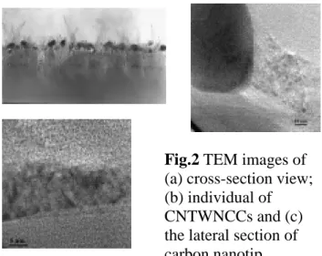
Figure 2 (a) reveals the TEM images of CNTWNCCs. Nanocrystalline chromium carbides are clearly embedded on the top of the carbon nanotips. Incidentally, sparse carbon nanotubes attached to the nanocrystalline chromium carbides are also observed. This is resulted from Cr film playing a catalyst role for
the growth of nanotubes. In TEM scope, nanotubes are rare to be seen. Fig. 2 (a) is intentionally displayed for showing the existence of nanotubes. This explains why there are no nanotubes in Fig. 1 (a). Now, we focus on activating the nanocrystalline carbides to make them act as catalysts and templates for the further growth of carbon nanotubes Thus, the field emission application could be significantly improved. Figure 2 (b) shows the individual carbon nanotips with nanocrystalline chromium carbide. Unlike hollow carbon nanotubes, Fig. 2 (c) shows that the carbon nanotips have a solid structure. Our previous work provides further information about carbon nanotips.
Fig.2 TEM images of
(a) cross-section view; (b) individual of CNTWNCCs and (c) the lateral section of carbon nanotip.
Figure 3 (a) shows a TEM image of an individual chromium carbide particle. The high-resolution TEM image depicts nanocrystalline chromium carbide. The diffraction pattern taken from the chromium carbide in Fig. 3 (b) also clearly proves its nanocrystalline structure. Further analysis of chromium carbides is performed by EDX technique. EDX spectrum provides a direct evidence of the chromium and carbon elements in chromium carbide.
Fig.3 (a) TEM
images; (b) diffraction pattern (DP) and (c) EDX spectrum of 0 5000 10000 0 100 200 300 C Cr Cr Cr EDX C o unt s Energy ( ev )
nanocrystalline chromium carbide, respectively.
Figures 4 (a) and (b) displays the I-V curve and F-N plot of CNTWNCCs. Plotting Ln ( I/V2 ) against 1/V ( F-N plot) should yield a straight line, implying that CNTWNCCs exhibit the property of field emission. A useful parameter for comparison with other field emitters is Eto
(turn-on field), which is the field V/d (applied voltage/ distance between cathode and anode) required to produce a current of 10 µA/cm2
. The
current density, which is 100 µA/cm2
as a function of time is further measured to determine the stability of the emitters. Experimental data reveal that the emitted light is brilliant and stable with a fluctuation less than 10 % in one hour. The I-V results clearly show that CNTWNCCs exhibit a favorable field emission property, that is, a turn-on field of 1.38
V/µm and 565 µA/cm2 at 2.2 V/µm. It is
attributed to the following reasons (I) good alignment and (II) high aspect ratio of nanotips. Besides, nanocrystalline chromium carbides are also expected to be the improvement in the field emission property. Due to the nanosize effect, the nanoparticles may offer higher electron-supply capability as well as better surface electrical conductivity of the CNTWNCCs as compared to those pure carbon nanotips.
Fig. 4 (a) The current density ( J ) versus
electric field ( E ) and (b) F-N plot of CNTWNCCs.
Growth Mechanism
Chromium carbide capped-carbon nanotip was synthesized using bias-assisted microwave plasma chemical vapor deposition. Such a material grew up to about several hundreds of nanometer long and tens of nanometer in diameter. The applied bias is a significant parameter in the growth process that the higher bias is effective to increase the growth rate.
However, the higher bias also contributes to a rapid formation of chromium carbide which leads to a shorter length of carbon nanotip at the same time. The higher ion energy also varies the tip diameter due to strong ion bombardment effect which is a competitor to deposition. It is found that the growth of chromium carbide capped-carbon nanotips reaches a limit due to the fully carburization of chromium.
Fig. 1 (a) Low magnification SEM image showing the uniformity of the vertical aligned chromium carbide capped carbon nanotips. (b) SEM image of a close view.
Fig. 2 TEM images showing (a) the cross-section view of chromium carbide capped carbon nanotips and, (b) high magnification view of an individual carbon nanotip and the inset shows the chromium carbide head.
Fig. 3 Schematic diagram of proposed growth model (a) Formation of nucleation process; (b) cap growth; (c) deposition of carbon (d) asparagus-like structure forms.
Fig. 4 Chromium carbide capped carbon nanotip grew under bias of -300 volt for 30 minutes
Chromium can be used as a catalyst to grow chromium carbide capped carbon nanotip with size of several tens of nanometers. Surface diffusion is believed to be the mechanism for the growth of carbon nanotip. The applied bias plays an important role that either assists the growth or etches the carbon away during growth.
H2 Plasma CH4, H2 Adsorption of carbon Diffusion of carbon (a) (b) (c) (d) 0.0 0.5 1.0 1.5 2.0 2.5 0 200 400 600 C u rr e n t de ns it y ( µ A / c m 2 ) Electric field ( V / µm ) 0.8 1.2 1.6 2.0 -12 -10 -8 Ln ( I / V 2 ) 1000 / V
In other words, the dimension of the chromium carbide capped carbon nanotip can be controlled. And there exits length limit which is due to the fully carburization of chromium. By supplying sufficient bias, an asparagus–like structure forms.
(c) Modification of Si Nano Emitters by Diamond - clad Process
The potential to achieve high-current devices is one of the most attractive issues of field emitters. In this work, needle-like Si tips with high aspect ratio is achieved by hydrogen plasma. Scanning electron microscopy (SEM) shows the average diameter and height of need-like Si tips are approximately 70 and 350 nm, respectively. To improve the field emission property of pure Si tips, the diamond-like carbon nanoparticles are further deposited on the top of the Si tips. Experimental results present that the diamond-like carbon-clad process improves the stability as well as the conductivity. Transmission electron microscopy (TEM) and Raman spectroscopy are used to observe their nanostructures and quality. Besides, the Auger electron spectrum also detects the partial growth of silicon carbide during modification process.
Fig. 1 (a) High and (b) low magnification of SEM photographs of Si nanotips
Fig. 2 TEM of (a) Si tips and (b) high-resolution images of individual Si tip.
Fig. 3 (a) High and (b) low magnification of SEM photographs of DLC-clad Si nanotips
Fig. 4 AES profile of DLC-clad Si tips.
Fig. 5 AES surface survey of DLC-clad Si tips.
Fig. 6 Raman spectrum of DLC-clad Si nanotips.
Fig. 7 Electric field (E) versus current density (J) of Si and DLC-clad Si tips, respectively.
According to the mentioned results, the major findings are summarized as follows:
1. The application of hydrogen plasma to induce Si tips is an easy method to produce high aspect ratio field emitters in many systems. 2. The average diameter and height of
needle-like Si tips are approximately 70 and 350 nm, respectively.
3. Due to the competition between deposition and etching rate simultaneously occurred in the plasma, the needle-like shaped of Si tips becomes blunt after DLC deposition.
4. Negative-bias effect is expected to enhance the growth rate of DLC during deposition. 5. Improvement on I-V characteristic of
DLC-clad Si tips is due to the negative electron affinity (NEA) property and carbon nanoparticles. 0.0 0.5 1.0 1.5 2.0 2.5 0 100 200 300 400 DLC-clad Si tip Si tip Cu rrent dens it y ( mA / cm 2 ) Electric field ( V /µm ) 6 0 0 9 0 0 1 2 0 0 9 8 2 In te n si ty ( a .u . ) W a v e n u m b e r ( c m- 1 ) β-SiC 9 0 0 1 2 00 15 0 0 1 8 00 2 10 0 1 35 5 .7 1 6 05 .9 7 In te n sit y ( a.u . ) W av e n u m b er ( cm-1 )
(d) Growth and purification of carbon nanotubes
Growth and Characterization of Multi-walled Carbon Nanotubes by Using
CH4-CO2 Gas Mixture
Carbon nanotubes were grown vertically and aligned on Fe catalytic nanoparticles deposited on a Si substrate at low temperature by using CH4 and CO2 gas mixtures, as shown in figure 1.
This is apparently different from the conventional reaction in gas mixtures of hydrogen and methane, hydrogen and acetylene, and hydrogen and benzene, etc.
Figure 1 (a) SEM image of carbon nanotubes in
a CO2-CH4 gas mixture with 96% of flow rate
ratio of CH4 /CO2 (b) SEM image of aligned
carbon nanotubes observed at 96% of the flow rate of CH4/CO2.
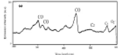
In microwave plasma deposition of CNTs, many reactions are involved in plasma and on substrate surface. A dynamic form of optical emission spectroscopy was used to detect the species in the plasma, as shown in figure 2. These data show the dominant species in gas phase reaction. The composition of plasma significantly affects the reaction mechanism of carbon nanotubes growth. We concluded that in
the CH4-CO2 gas system can increase the
amount of C2. In the C2-rich plasma the higher
excited C2 emission intensity is beneficial to
graphite deposition, and enhances carbon nanotubes synthesis on catalyst-deposited surface quality. Then a CNTs growth model in catalysts and gas environment of CH4-CO2 gas
mixture was investigated.
Figure 2. Emission spectra of growth CNTs
from microwave plasma observed in a CO2-CH4
gas mixture with CH4 /CO2 flow rate ratio of
96%.
Various catalyst, Fe, Ti, and Fe/Ti, were used to synthesize CNTs by CH4-CO2 gas sources.
Significant difference of morphology in the carbon deposition was observed among Fe, Ti and Fe/Ti catalyst, as shown in figure3. By proper adjusting growth parameters a high yield of vertically aligned CNTs can be found in Fe-deposited substrate, but Ti is not suitable as a catalyst in CNTs production.
Figure 3. The morphology of deposited carbon
using different metal catalysts (a) SEM image of carbon nanotubes grown on the Fe-deposited substrate. (b) SEM image of the carbon nanocones grown on the Ti-deposited substrate.
The effects of H2 plasma pretreatment on the
CNTs growth were investigated in the view point of CNTs morphology when Fe was used as the catalyst. After the H2 pretreatment, the
diameter of CNTs increased significantly as the H2 plasma pretreated time increased. Because of
the catalyst particle are sintering to enlarge the catalyst particles. However, the diameter of CNTs was governed by the catalyst particle size. The CNTs diameter distributed in the range about 10~20 nm when Fe-deposited substrate was not pretreated. But the diameter of CNTs changed from 30nm to 300 nm when Fe-deposited substrate was pretreated from 1 min to 15 min, as shown is figure 4. CNTs with various diameters by using MPCVD of CH4-CO2 gas mixture have good field emission
properties.
Figure 4. SEM images of vertically aligned
carbon nanotubes grown on a Fe-deposited
substrate (a) SEM image without H2 plasma
pretreatment. (b) pretreated with H2 plasma for
3 min
Vertically aligned CNTs with multi-walled structures were successfully grown at low
temperatures below 350oC by MPCVD using a
CH4-CO2 gas mixture. The low temperature
(a) 1μm (a) 2μm (b) 1μm (b) (a) 5μm (b) 1μm (a) 1μm
would be beneficial for reducing the diameter of CNTs but it will also decrease the growth rate on the substrate. Thus the CNTs grown at low temperature by the MPCVD using CH4-CO2 gas
mixture have good field emission properties.
Field emission from aligned carbon nanofibers grown in-situ by hot filament chemical vapor deposition
Our earlier report described the simplified CVD method for synthesizing carbon nanotubes. The apparatus used for synthesis is similar to that used to deposit CVD diamond. However, tungsten is the filament material most commonly used in diamond deposition. Here, an Fe-Cr wire is coiled as a filament to grow nanotubes and nanofibers. Such Fe-Cr wire is frequently used in furnace heating. The wire is not high-grade and has several impurities, being composed of Fe (72.43%), Cr (23.42%), Mn (3.45%) and Ni (0.69%). Deposition needed not be in vacuo, and process pressure was closed to the atmosphere. Carbon nanotubes and nanofibers were deposited on the Si substrate with CO2 as a carrier gas that passed through
ethanol. Different directions of flow of CO2
onto the substrate were adopted to confirm the effect of deposition conditions by adjusting the position of the gas inlet nozzle. The system used a 1 mm diameter Fe-Cr wire, and was heated by an A.C. current of 22 A at 40 V. In this experiment, the temperature of the filament was
approximately 1200℃, which was 100-200℃
lower than its melting point. The distance of the filament to the sample was 2 mm. The growth proceeded for 15 min.
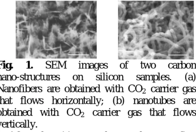
Fig. 1. SEM images of two carbon
nano-structures on silicon samples. (a) Nanofibers are obtained with CO2 carrier gas
that flows horizontally; (b) nanotubes are
obtained with CO2 carrier gas that flows
vertically.
After deposition, each sample was first visually examined. The surface of the sample near the bottom of the coiled filament was the blackest. The location of the nanofibers on the
sample was examined using scanning electron microscope (SEM). The images reveal that most nanofibers were near the bottom of the coiled filament. Figure 1(a) displays the SEM image of these nanofibers. These nanofibers were
produced when CO2 carrier gas flowed
horizontally to the substrate. Bundles of nanofibers are observed on the center of the substrate. The nanofibers have a high-aspect-ratio, implying good field emission characteristics. Figure 1(b) shows SEM image of nanotubes obtained using CO2 carrier gas
which flowed vertically toward to the substrate. A fixed CO2 flow rate of 15 sccm yielded two
completely different morphologies. Figure 1(b) shows a random tube network that consists of numerous curved tubes was formed; the tubes are 50-70 nm in diameter and a few tens of microns long. We supposed that flow direction should change the distribution and particle size of catalysts which originated from filament on the silicon sample.
The carbon nanofiber in Fig. 2 referred to Fig. 1(a) is clearly solid, in contrast to the hollow structure of the carbon nanotube. The insertion in Fig. 2 displays TEM image of an end section of an individual nanofiber. The structure is similar to that of a carbon-fiber, but with a nano-sized diameter. Under both grow conditions; the temperature of samples was almost the same (~700℃). Therefore, carbon nanofibers with a diameter of 10nm can be grown using this HFCVD method by just adjusting the direction of flow of the carrier gas. The fibers’ diameters are smaller than those obtained in other reports which mostly include diameters of 30–100 nm.
Fig. 2. Transmission electron microscope images of nanofiber,
obtained with CO2
carrier gas that flows horizontally.
Figure 3 displays the electron-emitting characteristics of the nanofibers obtained using a diode structure. An anode, ITO glass, was separated by 500 µm from the tip of the cathode made of nanofibers. The I-V properties was measured using an electrometer (Keithley 237) and analyzed through the Fowler-Nordheim
(F-N) model. The emission current at an applied
voltage of 1000V was 0.54 mA/cm2. The
macroscopic turn-on field, which is the field needed to extract current density of 10 µA/cm2, was 1.1 V/µm.
Fig. 3. Emission
current density against applied voltage and the F-N plot for the nanofibers,
obtained with CO2
carrier gas that flows
horizontally.
Density-controlled carbon nanotubes
It has been reported that field emission from a single multi-walled CNTs reaches 103 A/m2 , which is an order close to the upper limit of the conduction current to 104A/m2. These current densities are far beyond the field emission current density for practical field emission applications. Efforts have been made to improve the filed emission efficiency of CNTs, which includes purification or doping, but the most effective ways are decreasing the density of the CNTs. Methods like screen printing, anodic aluminium oxide (AAO) and plasma etching were used to tune the field emission behaviour while complicated procedures generates more problems. It has been reported that the density of CNTs plays a significant role in the field emission behaviours, and theoretical value of the optimal CNTs’ density was calculated as 2.5×10⁷ emitters/cm2 . The screening effect varies with the CNTs’ density drastically and the field enhancement is changed. In this study, CNTs’ density can be tuned by varying the catalyst’s composition or size and the density effect is confirmed experimentally.
Experimental details
Nickel and gold film with total thickness of 200 Å was deposited sequentially on Si wafers using an E-Gun Evaporator. The specimen was then introduced into a programmable furnace and anneals at a temperature of 900℃ and kept for two hours under argon atmosphere and then cooled to room temperature. The pre-treated substrates underwent bias-assisted microwave plasma chemical vapor deposition to grow the
CNTs. The microwave power was maintained at 400W with an external negative DC voltage supplied to the substrate. The total pressure in the chamber was kept at 2000 Pa with reactive gas of a mixture with H2/CH4=40/10 introduced
into the quartz chamber.
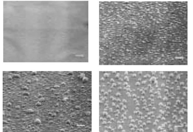
After furnace annealing, it was shown in figure 1 that the surface roughness increased and the catalyst film tend to form spherical particles as the composition of gold increase due to relief of surface energy. The catalyst particles gradually increased their size from flat surface to hundreds of nanometers in diameter. The increasing of the gold content lead to the decreasing of the nickel-gold alloy melting point and thus the particles size were increasing. It can be seen from the Ni-Au phase diagram that nickel and gold tend to dissolve to each easily, which means that the catalyst particle contains both nickel and gold. Although nickel and gold completely dissolve to each other at 900℃ and spinodal decomposition area exists, insufficient cooling rate may contribute to nickel-rich and gold-rich domains exists which is the main idea of growing CNTs (the nickel –rich domain) or not (gold-rich domain).
Fig.1 Surface morphologies with different film composition of (a) Ni 200Å(b) Ni 150Å ,Au 50Å (c)Ni 130Å, Au 70Å (d)Ni 100Å, Au 100Å, which show different surface roughness. The scale bar in the image is 1µm
Fig.2 SEM images of different density of CNTs
0 200 400 600 800 1000 0.0 0.2 0.4 0.6 Em is s ion c u rr e n t de ns it y ( m A/ c m 2) Voltage (V)
0 2 4 6 8 10 12 0.0 1.0x10⁻⁴ 2.0x10⁻⁴ (a) 20nm Ni (b) 15nm Ni 5nm Au (c) 13nm Ni 7nm Au (d) 10nm Ni 10nm Au C u rr ent D ens it y ( A /c m 2) Electric Field (V/µm) (a) 2.2×108cm-2 (b) 6.1×107cm-2 (c) 4.7×107cm-2
(d) 3.3×107 cm-2and the insets show the
corresponding cross section images. The scale bar in the image is 1µm.
The heat treated surface provided a template for further synthesis of different densities of CNTs. Figure 2 shows the surface morphology of different CNTs density with different heat treatment conditions. The CNTs grew to about 60 nanometers in diameter and several micrometers in length. Under the same conditions for CNTs’ growth, it was found that the CNTs preferred to grew around the catalyst particles as show in figure 1. It was reported that the island model formatted by pre-treatment of the catalyst was favourable for continuous CNTs’ film growth. The difference is that in this study, the gold or the Ni-Au solutions act as a CNTs growth inhibitor, which means the poor solvability of carbon in gold lead to a minor extrusion of carbon from the catalyst. The density therefore been reduced by the gold content which was unfavourable for CNTs growth and the increasing particle size which leads to fewer growth sites. Also, the bias in the microwave plasma chemical vapour deposition system provided a strong etching effect on the catalyst surface which resisted the CNTs nucleation. However, it was found that the catalyst provided a shield of ion bombardment to the bottom of the particles near silicon surface and nickel rich domains hence initiate the vapour-liquid-solid growth of the CNTs. More precise analyses still needs to be done in this complex system contain elements of silicon, oxygen, nickel and gold. The calculated CNTs densities of figure (a), (b), (c) and (d) are 2.2×108cm-2, 6.1×107cm-2, 4.7×107cm-2 and 3.3×107cm-2, respectively.
Figure 3(a) and (b) shows the TEM images of the CNTs obtained in figure 2 (a) and (c), respectively. The tubular structure with the encapsulated catalyst could be verified. Figure 3(a) shows the curved CNT where some curved CNTs on top of the vertical aligned CNTs could be found in figure 2(a). For the help of the EDS analysis in the TEM system, we found that the catalyst part of the CNTs contained detectable gold composition relative to the nickel. This phenomenon suggested that the gold content of
the catalyst resulted in the formation of pentagon and heptagon carbon rings, which due to different carbon solvability and lead to the winding CNTs to compensate the strain. However, the EDS analysis obtained from figure 3(a) shows no detectable gold content was found in the catalyst and straight CNTs were formed by the applied negative bias voltages.
Fig.3 TEM images of the CNTs showing (a)
the curved CNT consist of nickel and gold, (b) straight CNT consist of nickel.
In order to examine the effects of CNTs’ density on field emission properties, I-V measurement was utilized. Figure 4 shows the I-V curves measured with different CNTs density. Apparently, field emission efficiency was enormously improved relatively to the sample which continuous CNTs film was present. By decreasing the amount of CNTs, there was improvement in the emission current. The field emission efficiency should relate to two terms, which dense CNTs will reduce the enhancement factor while too low the density will cause poor emission sites. The best density of CNTs was unable to be acquired from the plot yet which the suggested value of 2.5×107cm-2 is not attainable in this experiment.
Fig.4 Field emission rom different densities of CNTs shown in figure 2.
Purification of multi-walled carbon nanotubes by microwave digestion method
In this work, a microwave-assisted digestion system was used to dissolve the metal catalyst. Inorganic acids such as H2SO4, HNO3 and HCl can rapidly absorb microwave heat and energy and completely dissolve metals that residue in carbon nanotubes. Since Environmental Protection Agency (EPA) recommended the microwave-assisted method with nitric acid, this leaching procedure of metals has been widely applied in sediments soils and sludge. Nitric acid is strong enough to solubilize metals from material.
The Co catalyst nanoparticles were deposited on p-type Si (111) wafer by sputtering method. Co catalyst was 7.5 nm in thickness. Experiments took place by electron cyclotron resonance chemical vapor deposition (ECRCVD). Mixture of CH4 and H2 was used as sources gas. Gas flow rates of CH4 and H2 were 18 sccm and 2 sccm, respectively. Power was set at 800 W. The reaction temperature was 600 °C. An acidic treatment in microwave digestion system (Milestone Microwave Labstation ETHOSD) was used to dissolve the metal catalysts. In this procedure, raw sample of MWCNTs were placed in a 100 ml Pyrex digestion tube. The first digestion step run at 210 °C for 20 min with a 1:1 mixture of 5 M HNO3 and 5 M HCl. The microwave power was set at 100 W. The second digestion step was carried out at 210 °C for 30 min. After digestion, the suspension was filtered with 0.1 mm PTFE (poly-(tetrafluoroethylene)) membrane in deionized water. After rinsing with alcohol and drying the sample, a black thin mat composed of MWCNTs was obtained.
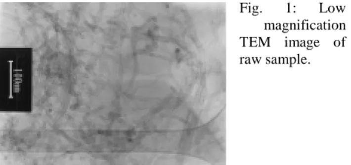
Fig. 1: Low magnification TEM image of raw sample.
Fig. 1 shows a low magnification TEM image of raw carbon nanotubes. In this image, there appeared impurities such as amorphous carbons, graphite and metals in multi-walled carbon nanotubes. Metal particles were evident embedded in the tip or in tube core of MWCNTs.
Many bundles with a diameter ranging from 10 to 30 nm can be observed in the TEM image.
Fig. 2: Low magnification TEM image of MWCNTs after purification by microwave digestion.
Fig. 2 shows a low magnification TEM image of MWCNTs after purification by microwave digestion. It indicated that most of the metal particles were removed. The structure and wall of MWCNTs were no destruction. It is well known that HNO3 is very efficient in solving metal particles and HCl is good in solving metal oxide. Amorphous carbon can be removed by nitric acid because it is a strong oxidant. However, in the microwave system, inorganic acid such as HNO3 and HCl rapidly absorbed microwave heat and energy without agitation and rapidly dissolved metals. The processing time of the two-step microwave-assisted and acid treated approach to dissolve metals in the MWCNTs was less than 1 h. In a microwave digestion system without agitation, heat was absorbed rapidly so that metal catalysts could be eliminated from MWCNTs rapidly with no damage.
Fig. 3 shows a TEM image of acid treated MWCNTs. It indicates the open end of MWCNTs, revealing that the cap is etched off and the wall of the graphite structure is not damaged. The diameter of tube is approximately 20 nm. So, lower concentration of acids and acid immersing time are available to completely retain wall of carbon nanotubes.
Fig. 3: HRTEM image of acid treated MWCNTs
The purpose of the combustion of acid treated samples is to purify CNTs according to the oxidation temperature difference between non-carbon nanotubes and CNTs. The burning temperature of CNTs is related to pre-treatment process and graphitization degree, so there is no general combustion temperature of CNTs. TGA is an effective method to detect the combustion temperature in air.
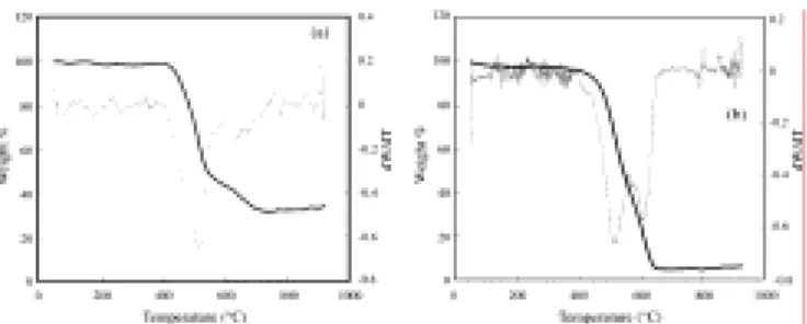
Fig. 4: (a) TGA graph of raw samples ranged from 30 to 900 °C at 20 °C/min under 10 sccm air flow rate. (b) TGA graph of the sample after microwave digestion acid-treatment ranged from 30 to 900 °C at 20 °C/min under 10 sccm air flow rate.
Fig. 4 shows TGA graphs of raw samples and purified MWCNTs. Fig. 4a shows the TGA of raw samples and indicates that the weight starts to reduce near 410 °C. The MWCNTs are completely evaporated at 730 °C. The remaining materials are metal catalysts, which are approximately 30% of the whole weight. The TGA graph indicates the existence of three phases in the sample. The differential TGA demonstrates a peak at 520 °C, which is suggested to be amorphous carbon and other small peak at 630 °C indicates that high temperature oxidation damages the MWCNTs.
Fig. 4b is the TGA graph of the sample after microwave digestion and acid purification treatment. After acid treatment, some water remained in the sample. It shows the correspondence between the slow weight loss from 30 to 450 °C and the loss of water and minor loss of amorphous carbon. In the temperature range from 450 to 650 °C, the weight decreases sharply to 5.25 wt.%. The peak at 520 °C in the differential TGA is assumed to be major weight loss of amorphous carbon and another peak at 610 °C indicates the damage of MWCNTs due to high oxidation. Combustion temperature of MWCNTs begins at 600 °C. The curve slope is maintained almost the same in the temperature range between 490 and 650 °C. It shows a constant combustion speed. After 650 °C the weight of MWCNTs remains constant, and the remainders may be metals and metal oxides, which reside inside the tube before combustion. So, the optimum amorphous combustion temperature is approximately 520 °C. The burning temperature of CNTs is related to pre-treatment process and graphitization degree, so it has little in common. TGA is an effective method to detect the combustion temperature in air. Dillon et al.
reported that the combustion temperature of carbon nanotubes is 785 °C by TGA. In their procedure, carbon nanotubes were synthesized by using laser vaporization method. The combustion temperature of raw carbon nanotubes synthesized by ECRCVD in our purification procedure begins at 520 °C. This conclusion is the same as that of Colomer et al. They reported the burning temperature in air is 500 °C for CNTs synthesized by catalystic chemical vapor deposition method.
14
Self-evaluation
For the favor of various bonding structure of carbon, several interesting tree-dimensional structure can be synthesized. In this project, basic carbon structures, including graphite, diamond, diamond-like, and nanotubes are synthesized with various appearances.
For graphite, it is possible to synthesize into ultra-sharp tips and fabricated into devices. Or by selecting catalyst, composite structure incorporating nanocrystals and nanotips can be form to further manipulate the electronic performance. For diamond and diamond-like which negative electron affinity nature make them good material for field emission, can be coated onto silicon tips. High efficient precursors of methane and carbon dioxide are suitable for synthesizing carbon nanofibers. For carbon nanotubes, catalyst contamination issue may be resolved by microwave digesting method. For practical use of field emission applications, the researches also provide a possible way to increase the field emission performance greatly.
More than twenty papers including conference papers are achieved by the financial support of the project. The presented results may contribute to the industry or science, while some may gives ideas for future researches.