國
立
交
通
大
學
資訊學院 資訊學程
碩
士
論
文
嵌入式異質多核心間溝通之效能實測與最佳化
Evaluation and Optimization of Inter-processor communication
for Embedded Heterogeneous Multi-core
研 究 生:李 松遠
指導教授:曹 孝櫟 教授
嵌入式異質多核心間溝通之效能實測與最佳化
Evaluation and Optimization of Inter-processor communication
for Embedded Heterogeneous Multi-core
研 究 生:李 松遠 Student:Sung-Yuan Lee
指導教授:曹 孝櫟
Advisor:Dr. Shiao-Li Tsao
國 立 交 通 大 學
資訊學院 資訊學程
碩 士 論 文
A Thesis
Submitted to College of Computer Science National Chiao Tung University in partial Fulfillment of the Requirements
for the Degree of Master of Science
in
Computer Science Sep 2009
Hsinchu, Taiwan, Republic of China
嵌入式異質多核心間溝通之效能實測與最佳化
學生: 李 松遠 指導教授: 曹 孝櫟 博士
國 立 交 通 大 學
資訊學院
資訊學程碩士班
摘要
近年來,異質多核心被大量應用於嵌入式系統中以解決耗電問題並增進系統 效能。然而異質核心間需要適當的溝通機制,才使得整個系統運作。先前的研究 發現這樣的核心間溝通機制(Inter-processor communication)將占去相當多的系統 資源,對於需要核心間頻繁溝通的應用程式來說,這樣的溝通程序將造成系統相 當大的負擔。因此在本研究中,我們透過一連串的實驗,量測與評估影響異質多 核心間溝通機制效能的各項參數。透過實驗的分析,我們得到一些建議設計與參 數,透過實際在一個嵌入式系統的案例上實作,發現所提之建議可以大幅降低 35%之處理器負擔,提升系統效能。 關鍵字:嵌入式系統,多核心處理器,異質多核心處理器,核心間溝通,效能評 估Evaluation and Optimization of Inter-processor
communication for Embedded Heterogeneous Multi-core
Student: Sung-Yuan Lee Advisor: Dr. Shiao-Li Tsao
Degree Program of Computer Science
National Chiao Tung University
Abstract
A heterogeneous multi-core processor composed of a general purpose processor (GPP) which handles the program flow and I/O and a digital signal processor (DSP) which processes mass data is widely used in an embedded system to improve the performance and energy efficiency. To exchange the data between a GPP and DSP, inter-processor communication (IPC) mechanism is required. In this paper, we evaluate the performance of the IPC for an embedded heterogeneous multi-core processor under different design strategies and parameters through a comprehensive experimental study. Based on the experimental results and findings, we further improve the IPC performance of a voice over IP (VoIP) phone as a case study. The experimental results demonstrate that the workload of the GPP significantly reduces 35% without scarifying the functionalities and voice quality of the VoIP system.
Key words: Embedded system, multi-core processor, heterogeneous multi-core processor, inter-processor communication, performance evaluation
Acknowledgment
本篇論文得到很多人的幫助才能夠完成,尤其是我的指導老師,曹孝櫟教 授,我從老師身上看到對於研究的專注態度與方法及生活中做人做事的原則,甚 至是老師在教學時的台風,都令我十分敬佩,他總是能在我陷入迷惘的時候指引 我方向,並總是適時的鼓勵我,使得我能夠繼續前進,非常感謝曹老師這幾年來 的指導。接著,我想要感謝我的論文口試委員,曾建超教授、林盈達教授與金仲 達教授,謝謝你們提供我許多寶貴的建議,讓我受益良多,同時也讓這篇論文得 以更加完善。 在實驗室的期間得到很多學長姊,同學,學弟妹的指導與協助, 在此特別謝 謝各位,另外感謝家父李文龍先生,家母張盛品女士,在日常生活對於我的關心, 能讓我安心的學習,最後,感謝每一個幫助過我的朋友,師長。Table of Contents
摘要...i
Abstract ...ii
Acknowledgment ... iii
List of Figures ...v
List of Tables ...vi
1. Introduction...1
2. Inter-processor communication mechanism and design parameters...4
2.1. Heterogeneous Multi-core Processor...4
2.2. Introduction to TI DaVinci DM6446...5
2.3. IPC mechanism for an embedded heterogeneous multi-core processor ....7
2.4. Design strategies and parameters of the IPC mechanism ...10
3. Performance Evaluation and Performance Measurement of Inter-processor Communication...12
3.1. Test Environments and Methodology...12
3.2. Hardware support and software modification...14
3.3. Big vs. Small Data Size Experiment...17
3.4. External vs. Internal Memory Experiment...18
3.5. Interrupt vs. Polling Experiment...20
3.6. Test Overhead ...21
4 Case study: VoIP...23
4.1 Case Introduction ...23
4.2 Case Test Results ...26
5 Conclusions...31
List of Figures
FIGURE 1. OMAP5912, A HETEROGENEOUS MULTI-CORE PROCESSOR 5
FIGURE 2. TMS320DM6446 DMSOC BLOCK DIAGRAM 6
FIGURE 3. GENERIC PROCEDURES OF AN IPC 8
FIGURE 4. MEASUREMENTS OF IPC PHASES 13
FIGURE 5. ESTIMATE THE DURATION OF A FUNCTION 15
FIGURE 6. CHECK THE CYCLE COUNTS IN THE PROC DIRECTORY. 16 FIGURE 7. MODIFY THE LINUX KERNEL TO ACCOMPLISH THE TESTS. 16 FIGURE 8. LATENCY IN MICROSECOND (ΜS) OF EACH IPC PHASE 18 FIGURE 9. COMPARISON OF IPC PERFORMANCE USING INTERNAL AND EXTERNAL
MEMORY AS THE SHARED MEMORY 19
FIGURE 10. THE LATENCIES OF INTERRUPT-BASED AND POLLING-BASED
NOTIFICATION MECHANISMS 21
FIGURE 11. PERFORMANCE EVALUATION PLATFORM OF THE VOIP SYSTEM 24 FIGURE 12. ARM AND DSP EXCHANGE DATA BY THE RING BUFFERS IN THE SHARED
MEMORY 25
FIGURE 13. G.711 CHARACTERS, G.711 PAYLOAD IN THE TCP/IP HEADER AND PACKET
INTERVAL VS. LAG 26
FIGURE 14. AN EXAMPLE OF THE CAPTURED PACKETS 28
List of Tables
TABLE 1. TI MS320DM6446 MEMORY 7
TABLE 2. COMPARISON BETWEEN STANDARD GETTIMEOFDAY() AND OUR OWN TIMER
DRIVER 15
TABLE 3. ARM WORKLOAD, INTER-PACKET ARRIVAL TIME AND ITS STANDARD
DEVIATION UNDER DIFFERENT IPC STRATEGIES 29
TABLE 4. ARM WORKLOAD AND NOTIFICATION UNDER DIFFERENT NOTIFICATION STRATEGIES 30
1. Introduction
Embedded systems usually handle both I/O jobs such as receiving and responding external events and computation jobs such as processing a large amount of data. To use either one general purpose processor (GPP) which provides better I/O controls or one digital signal processor (DSP) which offers rich computational resources to handle both I/O and computational jobs is usually less efficient [1]. In order to improve the energy and performance efficiency, a heterogeneous multi-core processor composed of GPPs and DSPs is thus widely used in an embedded system [2]. In a heterogeneous multi-core processor, inter-processor communication (IPC) mechanism is required for exchanging data and control messages between GPPs and DSPs. According to previous studies, the IPC mechanism is critical for a heterogeneous multi-core processor, especially for those embedded systems involving frequent interactions between the two processors [3][4][5].
A number of studies have evaluated the IPC performance of a heterogeneous multi-core processor. Gorgonio et al. [3] and Chiu et al. [4] examined the IPC overhead and the performance of a task running on a GPP or DSP. Since the IPC introduces a considerable overhead, it is not always efficient to assign computation-intensive tasks to the DSP through the IPC. Their experimental results help the designers to map their tasks to the GPP and DSP efficiently. Luiz et al. [5] further proposed a formal model based on the timed automata for the IPC of a heterogeneous multi-core processor. Their model helps the designers to understand the IPC mechanism. Several hardware and software improvements have been proposed for the IPC mechanism of a heterogeneous multi-core processor. Chen et al. [6] proposed a new bus architecture to speed up the IPC between GPPs and DSPs. For
the IPC improvements through software technologies, Kluter et al. [7] suggests using the scratchpad memory, i.e. the internal memory, instead of the external memory as the shared memory for the IPCs. The IPC performance by using internal shared memory is significantly improved, especially for streaming applications which involve frequent IPCs between GPPs and DSPs. Brisolara et al. [8] presented a method, called “Message Aggregation”, to aggregate several IPC requests into one single request and reduce the number of IPCs between GPPs and DSPs. This technique also considerably reduces the IPC overhead.
Unfortunately, previous studies did not consider above design factors together and investigate and compare the IPC performance under different design strategies and parameters. In this paper, we establish an experimental environment and evaluate the IPC mechanism through an experimental study. Based on experimental results and findings, we apply appropriate IPC strategies and parameters to a case study, i.e. a VoIP phone, to improve its performance. Experimental results indicate that with the proposed improvements, the CPU workload could reduce 35% without scarifying the functionalities of the VoIP phone. The main contributions of this paper are to provide an experimental study of the IPC mechanism for an embedded heterogeneous multi-core processor and compare the IPC performance under different design strategies and parameters. The results offer designers a guideline in choosing the appropriate IPC designs and parameters for an embedded system using a heterogeneous multi-core processor.
The rest of the paper is organized as follows. Section 2 briefs the IPC mechanism, and presents different IPC design strategies and parameters. Section 3 introduces the performance evaluation environment, methodologies and results. Based on the experimental results and findings, we then apply appropriate IPC designs to a case
study, i.e. VoIP phone. The experimental results are presented and discussed in Section 4. Finally, we conclude this study in Section 5.
2.
Inter-processor communication mechanism and
design parameters
2.1. Heterogeneous Multi-core Processor
Currently, the embedded system is requested for more functions and faster execution speed. If the embedded system just use one general purpose processor to do all the tasks, including code flow, I/O and complicated computation, it will incur the low-performance and power-consumming. The DSP wich is good at computation is added into the system in the current design. The control and computation tasks are separated by this kind of architecture. The cores with different characters will process their appropriate tasks. The architecture is constitute of the “Heterogeneous multi-core processor”.
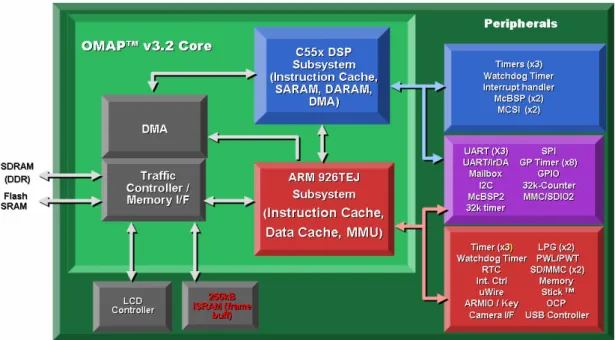
Figure 1 illustrates the block diagram for the OMAP5912 [9]. There is an ARM926 for task control and a TMS320C55X DSP for data computation. The two elements consist of a heterogeneous multi-core processor.
Figure 1. OMAP5912, a heterogeneous multi-core processor
2.2. Introduction to TI DaVinci DM6446
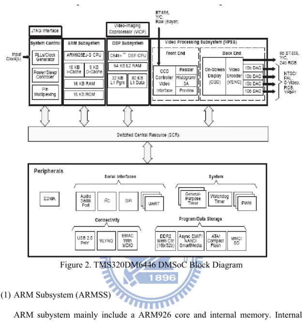
The dual-core architecture of the TI DaVinci DM6446 [10] provides benefits of both DSP and Reduced Instruction Set Computer (RISC) technologies, incorporating a TMS320C64x+ DSP core and an ARM926EJ-S core. The ARM926 EJ-S core, which OS typically runs on it, generally performs user interface and other functions. The TMS320C64x+ DSP features high performance and low power consumption and is usually in charge of high-computation and real-time jobs. It will be a powerful embedded processor to take advantage of the ARM and DSP cores.
The hardware design of TI DaVinci mainly includes three parts. They are ARM Subsystme、DSP Subsystme and the related equipments about external memeory (eg: DMA、DDR2 and External Memory Interface). Figure 2 shows the TMS320DM6446 DMSoC block Diagram.
Figure 2. TMS320DM6446 DMSoC Block Diagram (1) ARM Subsystem (ARMSS)
ARM subystem mainly include a ARM926 core and internal memory. Internal memory are 16KB instruction cache 、 8KB data cache 、 16KB RAM and 8KB ROM. Except cache, DSP can access internal memory , so they could be one of share memory to commmunicate between ARM and DSP.
(2) DSP Subsystem (DSPSS)
C64x+DSP、Video-Imaging Coprocessor (VICP) and internal memeory are consist
of DSP subsystem. The internal memeory includes 32 KB L1 Program RAM、80 KB L1 Data RAM and 64 KB L2 RAM. ARM can access L1 and L2 internal memeory of DSP. The internal memeory also can be used as the share memeory between ARM and DSP.
(3) Related equipments about external memeory
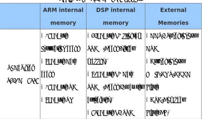
These parts includes DDR2 SDRAM, FLASH, CF and External Memory Interface.These memory equipments are not in the inside of ARM or DSP, but ARM or DSP still can be accessed them by external memory interface. Table 1 shows the memory overview of the TI MS320DM6446.
Table 1 shows the memory summary of the TI DaVinci. Table 1. TI MS320DM6446 memory ARM internal memory DSP internal memory External Memories TI DaVinci MS320DM6446 * 16K-Byte Instruction cache * 8K-Byte Data cache * 16K-Byte RAM * 8K-Byte ROM * 32K-Byte L1 Program SRAM/Cache(direct mapped) * 80K-Byte L1 Data SRAM/Cache(2-way set associated) * 64K-Byte L2 SRAM * DDR2 Synchronous DRAM * Asynchronous EMIF/NOR/NAND Flash * ATA/Compact Flash(CF)
2.3. IPC mechanism for an embedded heterogeneous multi-core
processor
The generic procedures of the IPC mechanism of a heterogeneous multi-core processor compose of ten steps which are shown in Figure 3. When the system starts, the GPP program first downloads the DSP programs to the DSP internal memory so that the DSP programs can execute when the GPP program invokes the DSP functions.
Once the GPP program has a job to assign the DSP, it makes a DSP function call in the DSP library. The DSP library then initiates an IPC which transfers the control message and data to be processed to the DSP.
GPP
DSP
Data buffer Data bufferShared
Memory
1
3
5
10
6
8
9
2
4
7
Interrupt
or
Polling
Control messages Figure 3. Generic procedures of an IPCDuring the IPC, the GPP first copies the data to be processed by the DSP to the shared memory which can be accessed by both the DSP and GPP in step n. Then, in step o, the GPP prepares a control message which indicates the information of the request such as the address and length of the data and the DSP function that the GPP program invokes, and also stores the control message in the shared memory. The control messages could be structured as a list so that the GPP program could consecutively create new requests to the DSP and the DSP could process the DSP function requests one by one. The format and address of the control message in the shared memory shall be known by both the GPP and DSP before the IPC so that they
could communicate to each other through the control messages. In step p, the GPP uses an interrupt or other mechanisms to notify the DSP that the GPP program has a DSP function request to the DSP. The DSP is notified and reads the control messages from the list in step q. The DSP finds the data to be processed based on the control message in step r and then starts to process the request. After the DSP finishes the job, the DSP has to copy the processed data to the shared memory in step s so that the GPP could access the results. Similar to the procedure that the GPP notifies the DSP, the DSP also has to prepare a control message indicating the address and length of the processed data in the shared memory in step t. Finally, the DSP uses an interrupt or other means to notify the GPP in step u. The GPP is notified and reads the response message in step v. Then, the GPP program could get the processed data in step w.
After the GPP program call the DSP function, the GPP program could either wait for the DSP function return or sets a call-back function. If the GPP program waits for the DSP return, the GPP program is blocked for a while. Otherwise, if the GPP program sets a call-back function, the GPP program could continue processing other jobs without blocking. Once the DSP function is complete, the GPP program is notified by an interrupt and then a call-back function which can handle the DSP return. As can be seen from the above description, the IPC introduces extra GPP and DSP workload to handle memory copies, process request, response messages, interrupts, and notifications. In the next subsection, we discuss the IPC design strategies and parameters which may influence the IPC performance.
2.4. Design strategies and parameters of the IPC mechanism
The first design consideration for an IPC is the granularity of the IPC requests between the GPP and DSP, i.e. the size of the data block to be passed from the GPP to the DSP. One possible design choice is to merge several DSP function calls and their associated data blocks together and invoke only one IPC [8]. The number of IPCs and the IPC overhead are both reduced. However, in that case, more shared memory space is required to store the data blocks to be processed, and the response time of the DSP function call may increase since function calls may be deferred, merged and sent to the DSP together.
Another design strategy is to utilize different types of the shared memory for the IPC data exchanges. One common approach is to use the external SDRAM attached to the system bus as the shared memory. Another possible choice is to expose the GPP internal memory to be accessed by the DSP or vice versa. Using the internal memory as the shared memory could significantly speed up the memory access by the GPP and DSP [7] so that the IPC can be speeded up. However, the size of the internal memory is much smaller than that of the external memory, and the cost of the internal memory is much expensive than that of the external memory. The internal memory should be carefully managed to maximize the cost-efficiency of the embedded system.
Another design consideration is to use the interrupt or polling mechanism for the GPP and DSP to notify the other processor. The common approach is to use an interrupt for the GPP and DSP to notify the DSP and GPP, but the interrupt involves interrupting the handling process and results in a considerable overhead. For example, a portable media player or voice over IP (VoIP) phone periodically calls DSP functions to compress and decompress voice and video frames. The IPC overhead is significant if the interrupt notification is used. Another approach is to use the polling
mechanism for the notification. The polling mechanism does not use an interrupt to notify the other processors. It simply sets and resets a flag in the shared memory when the request and response messages and data blocks are ready in the shared memory. For example, after step n and step o, the GPP sets a flag in a particular address in the shared memory. The DSP periodically checks the flag by reading the memory address and sees if there is a new request from the GPP. If the flag is set, the DSP reads the request message, and processes the data. The overhead to read an internal memory address is much less than an interrupt handling routine. However, one major challenge of this approach is how the DSP and CPU know the time to poll the flag. If the DSP or GPP has to poll the flag very often, the overhead also increases. On the other hand, the delay increases if the DSP or GPP polls the flag infrequently. Therefore, this polling notification approach is more suitable to the embedded systems with periodical IPCs. For example, if a VoIP phone produces and consumes voice frames every 20ms, the polling interval of the IPC could be set as 20ms so that the notification overhead and the IPC response time could be both reduced.
3. Performance Evaluation and Performance
Measurement of Inter-processor Communication
3.1. Test Environments and Methodology
In order to examine the detail IPC performance under different design parameters, an evaluation platform is established. TI DaVinci DM6446 [9] which has an ARM926EJS and C64x+ DSP is used for the experiments. Embedded Linux and DSP/BIOS are running on ARM926EJS and TI C64x+ as the operating systems. Then, ARM programs and DSP programs can execute on top of Embedded Linux and DSP/BIOS. Programs on Embedded Linux call DSP functions through the DSP library. The DSP library further utilizes the DSP/BIOS LINK [11] which implements the IPC to transfer the request to the DSP. The DSP/BIOS LINK is a Linux kernel driver and can communicate with the DSP/BIOS to complete the IPC task.
To evaluate the IPC mechanism, we develop user-space testing programs on the ARM and DSP. We also modify the DSP/BIOS LINK in Linux so that the IPC procedures can be tracked and the latency for each IPC phases could be gathered. In this study, we only measure the IPC performance from the ARM processor’s point of view. This is mainly because that the DSP usually serves as a slave co-processor and dedicate in processing the data. On the other hand, the ARM processor usually handles multiple tasks and the developers are more concerned about the IPC delay on the ARM or the ARM resources occupied by the IPC.
Therefore, we divide the IPC into five major phases as shown in Figure 4 and measure the latency of each phase. During phase (A), the ARM program copies the data block to be processed to the DSP from a user space memory to the kernel space memory. The kernel space memory could be the shared memory space that both the
ARM and DSP can access so that additional memory copy in the kernel space is avoided [12]. Phase (A) corresponds to step n shown in Figure 3. Phase (B) is to prepare the control message and send an interrupt to the DSP. Phase (B) corresponds to step o and step p. Phase (C) composes of all the DSP procedures during an IPC. Phase (C) includes that the DSP is interrupted, and the DSP/BIOS receives the request, the DSP programs perform the requested functions, and responses the request. Phase (C) corresponds to step q to step u shown in Figure 3. Phase (D) is the interrupt handling procedure for receiving the response and corresponds to step v of Figure 3. Finally, phase (E) involves a memory copy of the result from the kernel space to the user space. Heterogeneous multi‐core processor (TI DaVinci DM6446) ARM program Embedded Linux ARM DSP program DSP/BIOS DSP
A
B
D
C
E
3.2. Hardware support and software modification
To get the time period of every step, we need hardware support and software modification.
z Hardware timer
To measure the performance of communication between cores, it has to measure the time period between the ARM and DSP. Many embedded systems support the hardware timer for profiling use. The TI DAVINCI supports two 64-Bit general-purpose timers and one 64-Bit watch dog Timer. The resolution of the hardware timers is 27MHZ. We will take advantage of the hardware timer as one of our measurement tool. The test begins from the application of the user space. The user application can not access the hardware timer directly. We need to write a driver to access the hardware timer in the Linux kernel space and a system call for getting the time periods from user space into the kernel.
z /proc file system
Hardware timer provides the accurate measurement. However, the test needs many times to access hardware timer during a test. The time measurements of accessing hardware timer in the test have to temporally save in somewhere. After the test finished, we can get the time to calculate the duration of every period. To make the test more accurate, the whole test results will saved in the /proc file system. We have to add a new directory in /proc file system to save the time periods.
z Implement drivers to complete the test
In order to precisely measure the latency of each IPC phase and minimize the instrument overhead, we implement our own timer driver instead of using standard
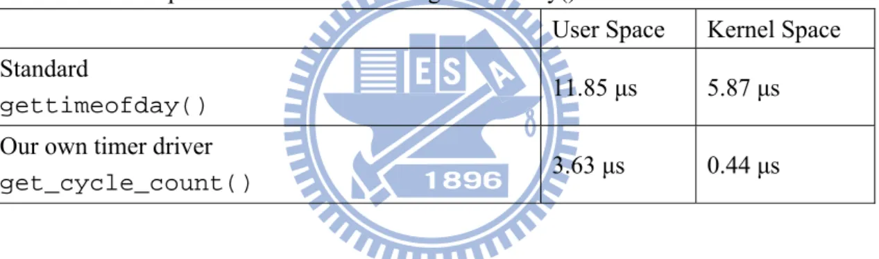
gettimeofday() library in the Linux kernel and user programs. Standard gettimeofday() library in Linux provides microsecond(μs)-level accuracy, but our own timer driver which utilizes the TI DaVinci 64-Bit general-purpose timer can offer 1/27 μs precision. Moreover, the overhead to retrieve the timer is significantly reduced. Table 2 shows the comparison between the standard gettimeofday() library and our own timer driver. Since we insert timer retrieval codes in the testing program and kernel codes to gather the latency of a specific procedure, we therefore deduct the instrument overheads, i.e. the extra delay to access the timer, from the measurement results shown below.
Table 2. Comparison between standard gettimeofday() and our own timer driver
User Space Kernel Space
Standard
gettimeofday() 11.85 μs 5.87 μs
Our own timer driver
get_cycle_count() 3.63 μs 0.44 μs
We need to implement some drivers to access the hardware timer and /proc
directory processing. Now, we take an example to explain the measurement and get the results. If we want to measure the duration of the function ABC( ), the
get_cycle_count( ) function which gets the clock cycle count from hardware timer will
be inserted into the code. Figure 5 illustrates this case.
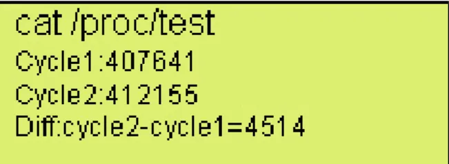
The time measurement results will save in the /proc/test. The test directory is added when the test initialization.After the test finished, check /proc/test to get the duration of ABC( ). Figure 6 demonstrates the example. For instance, a test directory is added into the /proc directory. After the test is executed, there will be some records about the clock cycle counts from hardware timer.
Figure 6. Check the cycle counts in the proc directory.
Then, we will calculate the time period from clock cycle counts to microseconds. At last, figure 7 demonstrates what we add in the system to accomplish the tests.
3.3. Big vs. Small Data Size Experiment
A number of experiments are conducted to evaluate the IPC performance under different design strategies and parameters. The first experiment considers different sizes of data blocks to be passed to the DSP. An ARM program sends data blocks in different sizes to the DSP, and the DSP program returns the results to the ARM. Since we only concern the IPC performance, we assume the DSP testing program does not process the data and simply responses the request with the same data block to the ARM. In this experiment, we use the interrupt to notify the ARM and DSP when the ARM requests or the DSP responses the request. Also, we use the external SDRAM as the shared memory. Figure 8 illustrates the latency for each IPC phases under different block sizes. The x-axis lists the five IPC phases shown in figure 4. The y-axis shows the latency of each phase in microsecond (μs). As can be seen, the IPC spends a large portion of the time in phase A and phase E which performs data copies between user memory and kernel memory. The latency of Phase A and Phase E depends on the block size. Phase B and Phase D are to process control messages and response messages and to handle interrupt-based notifications. Phase C consumes merely 70μs-80μs since in this experiment, the DSP program does not perform any task, and just replies the request with the same data block. The experiment results indicate that if the block size is small such as 128bytes, the control message process and notification overhead, i.e. phase B and phase D, are significant. The overhead of the interrupt notification is similar to the memory copy overhead for the IPC with small data block. On the other hand, if we could combine multiple requests and data blocks through less number of IPCs, the overall IPC performance can be improved. For example, to exchange a total of 32K data block between the ARM and DSP through 32 1Kbyes IPC, 2 16Kbytes, 1 32Kbytes IPCs spend 34ms, 10ms, 8ms,
respectively. A B C D E 128 bytes 148.8 131.2 73.5 114.4 143.8 1K bytes 416.6 132.5 73.0 114.3 405.3 16K bytes 2188.5 131.6 78.6 111.9 2160.7 32K bytes 4121.6 131.4 81.7 115.4 4101.7 0.0 500.0 1000.0 1500.0 2000.0 2500.0 3000.0 3500.0 4000.0 4500.0 mi cr os e con d
Figure 8. Latency in microsecond (μs) of each IPC phase
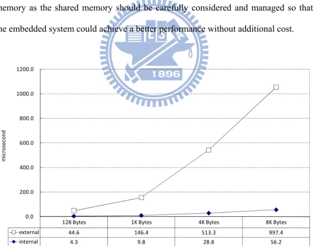
3.4. External vs. Internal Memory Experiment
The second experiment considers different types of memory, i.e. internal memory and external memory, as the shared memory for exchanging IPC data blocks. In this experiment, we use the ARM internal SRAM as the internal memory and use the SDRAM as the external memory. The two memory areas can be both accessed the two processor cores. The latency of the memory accesses mainly influences phase A and phase E which performs memory copies. This experiment only measures the delay in the kernel space to copy different sizes of data blocks from the user space memory to the internal or external memory. The result is less than the data shown in Figure 8 since the delay shown in Figure 8 includes the latency for executing user lib,
system call, and kernel code to handle the memory copy. Figure 9 only illustrates the latency for memory copies in the kernel space. Obviously, the memory copies in the internal memory are much faster than that in the external memory. In other words, the IPC using internal memory as the shared memory is faster than that using external memory as the shared memory. The latency depends on the data block sizes. For example, the latency to copy an 8Kbytes data block from the user space to the ARM internal SRAM reduces 94% time comparing with that to the external SDRAM. This experiment indicates that to use internal memory as the shared memory considerably improves the IPC performance, especially for exchanging large IPC data blocks. However, internal memory is expensive and usually small. To use the internal memory as the shared memory should be carefully considered and managed so that the embedded system could achieve a better performance without additional cost.
128 Bytes 1K Bytes 4K Bytes 8K Bytes
external 44.6 146.4 513.3 997.4 internal 4.3 9.8 28.8 56.2 0.0 200.0 400.0 600.0 800.0 1000.0 1200.0 mi cr o sec o n d
Figure 9. Comparison of IPC performance using internal and external memory as the shared memory
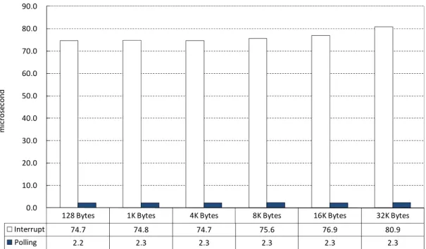
3.5. Interrupt vs. Polling Experiment
The interrupt-based notification mechanism introduces serious overhead for the IPCs with small data blocks. Therefore, the next experiments uses the polling-based mechanism to notify the ARM and DSP instead of using interrupt-based approach. To implement the ARM and DSP notification mechanism using the polling approach, we use a flag. When the ARM notifies the DSP, it sets the flag in the shared memory. The DSP could periodically check the flag and if the flag is set, the DSP process the request. After the DSP completes the task, it resets the flag. The ARM could also periodically poll the flag and if the flag is reset, the ARM knows the DSP task has been finished and could retrieve the results. In this experiment, since the DSP program does not perform any job, the ARM performs a busy waiting loop to check the flag and see if the DSP ask is complete or not. Another implementation approach for the polling-based notification is to periodically check the flag. If the ARM or DSP find the flag is not set or reset, it performs other jobs. Otherwise, it processes the IPC requests or results.
Figure 10 compares the interrupt-based notification and polling-based notification under different block sizes. The results show that the notification mechanism is independent of the IPC bock size. Also, the polling-based notification approach significantly reduces 95% overhead compared with the interrupt-based notification approach. For these embedded applications which generate frequent and periodical IPCs with small block sizes, polling-based notification approach is a better design choice. We use the VoIP phone as a case study and consider these design considerations in improving the IPC performance of the VoIP phone.
128 Bytes 1K Bytes 4K Bytes 8K Bytes 16K Bytes 32K Bytes Interrupt 74.7 74.8 74.7 75.6 76.9 80.9 Polling 2.2 2.3 2.3 2.3 2.3 2.3 0.0 10.0 20.0 30.0 40.0 50.0 60.0 70.0 80.0 90.0 m ic rose cond
Figure 10. The latencies of interrupt-based and polling-based notification mechanisms
3.6. Test Overhead
Because we add a measurement function into the original code during the test, the section will check the overhead of the function.
According to table 2 shows that accessing the hardware timer from user space is longer than that from kernel space. It is reasonable because accessing timer from user space needs the system call to get into the kernel space. Then, application in the user space can access hardware timer by the system call.
According to the figure 4, there will be totally 6 times which include 2 times from user space and 4 times from kernel space to access timer in the whole test. The effects to the smallest data size 128 bytes and the largest size 32Kbytes illustrate as following:
148.77+131.22+75.51+114.37+143.77=613.64 μs (total time in data size test of 128 bytes)
4121.62+131.37+76.66+115.37+4101.7=8546.72 μs (total time in data size test of 32K bytes)
Test overhead in 128 bytes 9.02/613.64=1.47% Test overhead in 32K bytes 9.02/8546.72=0.105% Test overhead < 1.5%
We get the test overhead in 128 bytes is about 1.47% and 32Kbytes is about 0.105%. It explains the time measurement doesn’t twist the original behavior in the communication test.
4 Case study: VoIP
This chapter will take advantage of the measurement method provided by chapter 3 for a real application. For a heavy loading processor, if the more utilization can be squeezed, the more jobs can be processed. The utilization of a processor is an important resource for the embedded system.
4.1 Case Introduction
Above experiments reveal that depending on the characteristics of an embedded system, the embedded system using a heterogeneous multi-core processor may prefer different IPC strategies and parameters which significantly influence the IPC performance. In this section, we apply different IPC strategies and parameters to a VoIP phone and evaluate its performance. VoIP phone is an embedded system and usefully uses a heterogeneous multi-core processor. The GPP usually runs a VoIP client and the DSP compresses and decompresses voice packets. The IPC frequently occurs between two processors, e.g. every 20ms, and the size of the IPC data block is usually small, e.g. 160bytes. The IPC occupies a significant part of the GPP resources for the VoIP system. Therefore, we apply suitable IPC designs to the VoIP system and improve the IPC performance.
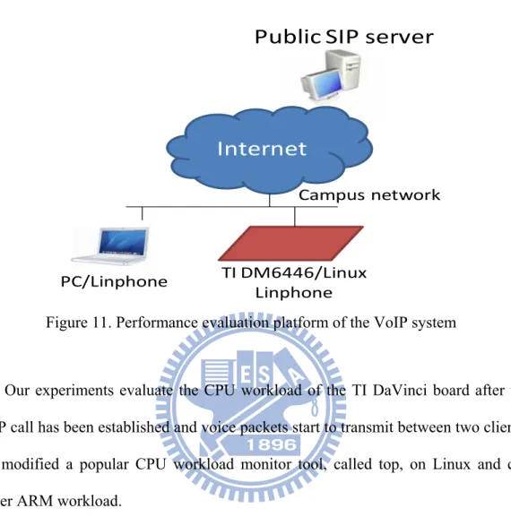
Our experimental environment is shown in figure 11. We establish a VoIP test-bed which composes of a public SIP [13] server which handles VoIP calls and two client nodes which can establish a VoIP communication. One VoIP client runs Linphone[14], an SIP user agent, on a PC and the other VoIP client uses TI DaVinci DM6446 evaluation board. We port and modify Linphone on the embedded evaluation board and evaluate its performance. The two VoIP clients first run and
the SIP server.
Internet
Public SIP server
Campus network PC/Linphone TI DM6446/Linux LinphoneFigure 11. Performance evaluation platform of the VoIP system
Our experiments evaluate the CPU workload of the TI DaVinci board after the VoIP call has been established and voice packets start to transmit between two clients. We modified a popular CPU workload monitor tool, called top, on Linux and can gather ARM workload.
The VoIP client application running on the ARM processor periodically calls the DSP function to encode and decode voice frames. For example, if G.711 codec is used, the VoIP client has to call the G.711 library every 20ms for decoding and encoding voice packets. According to our experiments, the polling-based notification approach is preferable if the application has periodical IPCs with small block sizes. Therefore, we modify the DSP/BIOS LINK to support polling-based notification and compare its performance with the conventional interrupt-based approach. To implement the polling-based notification on the ARM processor, the ARM processor prepares the control messages and data blocks in the shared memory and set a flag. Once the DSP
finishes the task, it resets the flag in the shared memory. The ARM program sets a polling timer after it sends the request to the DSP. When the polling timer expires, the ARM program checks the flag. If the flag is reset, the ARM understands the task has been finished, and then could access the results in the shared memory. Since the ARM and DSP programs perform their own tasks asynchronously, we therefore have to prepare a number of blocks in the shared memory so that the ARM program could continually generates the requests and the DSP program could process the requests. The blocks in the shared memory are implemented as ring buffers.
Figure 12 shows ARM and DSP exchange data by the ring buffers in the shared memory.
Figure 12. ARM and DSP exchange data by the ring buffers in the shared memory
Another important characteristic of the VoIP application is the small packet size. For example, the voice frame of G.711 is 1280 bits, i.e. 160 bytes. The packet size becomes smaller if we choose other low-bit-rate codecs such as G.723. The data block size is small so that it is affordable to use internal memory for exchanging IPC data. Thus, we use the internal memory rather than the external memory for the IPC.
The voice processing algorithm is G.711 in the tests. Figure 13[15] shows the characters of G.711. According to the G.711, the packet inter-arrival time is about 20 ms and voice data is 1280 bits (=160 bytes).
Figure 13. G.711 characters, G.711 payload in the TCP/IP header and packet interval vs. lag
4.2 Case Test Results
Table 3 illustrates the ARM workload under different IPC strategies. In the first design strategy (denoted as ARM), we only use the ARM processor to handle both the VoIP client and the voice codec. In other words, the DSP does not involve. This approach consumes the ARM processor 47% CPU resource. In the second design
strategy (denoted as ARM+DSP+Int+Ext), the DSP is involved and handles the voice codec. Then, the IPC is required. In this design strategy, the IPC uses the external SDRAM as the shared memory and uses the interrupt-based mechanism for IPC notifications. This approach significantly reduces 50% of the ARM workload. The third configuration (denoted ARM+DSP+Pol+Ext) uses the polling-based mechanism to replace the interrupt-based mechanism. The ARM program initiates a 20ms polling timer to periodically check the completeness of the DSP task. The experiments indicate that the ARM workload could be further reduced 10% if polling-based notification is used. In the fourth configuration (denoted as ARM+DSP+Interrupt+Internal), we use the internal memory as the shared memory. Compared the design strategy 2 and 4, we find that the ARM program improves 28% if the internal memory is used for the IPC shared memory for the VoIP phone. For an embedded system involving small IPC packets, to use internal memory can significantly improves the IPC performance. Finally, we apply both internal and polling-based technologies in the fifth configuration (ARM+DSP+Polling+Internal). Experimental results indicate that we could reduce 35% ARM workload if we use both polling-based notifications and the internal memory.
To use polling-based notification mechanism, the latency that the ARM can detect the completeness of the DSP function may suffer from extra delay compared with the interrupt-based approach. This is because the interrupt-based mechanism could interrupt the ARM processor as soon as the complete of the DSP function. However, the ARM processor has to wait for the next polling timer if the DSP resets the polling flag just after the ARM checks the flag. One may concern that if we use polling-based approach instead of the interrupt-based approach, the voice over IP application may have extra packet delay and/or packet delay jitters. Therefore, we use
Wireshark[16] running on the receiver VoIP client to measure the packet arrival time. The figure 14 and figure 15 show the example of captured packets in the experiment.
Figure 14. An example of the captured packets
Check the time, protocol and payload columns in figure 14. These show that the packets captured meet the characters of G.711. It explains our modification didn’t make the wrong behavior or side effect in the application layer.
Table 3 also shows the experimental results. Our experimental results show that the polling-based approach does not introduce additional packet jitters, and provide the same voice quality. This is mainly because most of the current VoIP client maintains a receiving buffer with 2-3 voice packets to accommodate the network jitter. That implies the packets arriving to the receiver are played immediately. Therefore, jitter buffer which is usually 2 to 3 voice packets, i.e. 40ms to 60ms, accommodates the IPC notification delay. Since the polling-based approach does not introduce additional network jitter. The proposed approach which uses internal memory and pooling approach can reduce 35% ARM CPU workload without scarifying the VoIP functionalities and voice quality.
Table 3. ARM workload, inter-packet arrival time and its standard deviation under different IPC strategies
ARM workload (%) Inter-packet arrival time (ms) Standard deviation of the inter-packet arrival time ARM 46.53 20.45 0.48 ARM+DSP+Intr+Extl 22.73 20.40 0.40 ARM+DSP+Poll+Extl 20.92 20.19 0.35 ARM+DSP+Intr+Intl 16.37 20.07 0.11 ARM+DSP+Poll+Intl 14.84 20.24 0.17
As mentioned before, the ARM processor may not be able to know the completeness of the DSP tasks immediately when the polling-based approach is used. Although this polling-based mechanism does not influence the applications which
could accommodate the latency, some real-time embedded system may need a guaranteed response time of the DSP task. Then, we evaluate the notification latency by applying polling-based approach. We evaluate the notification latency use the same VoIP programs. Table 4 shows the notification latencies and corresponding ARM workload when we configure polling interval as 5ms, 10ms, 15ms to 20ms. As can be seen, the CPU workload increases if we configure frequent polling timers. Also, the notification latency decreases when we configure frequent polling timer. Table 4 shows that when we configure 5ms polling interval; the ARM workload increases but the notification latency cannot decrease. This is because the DSP programs spend about 6ms to process the task. If we poll the flag every 5ms, we have to poll twice and then can know if the task is completed or not. Therefore, the notification latency if we configure 5ms polling interval is about two polls, i.e. 10ms. One efficient approach for the polling-based approach is to estimate the DSP function latency, and polling the flag after the DSP can complete the task. Interrupt has the advantage of very low latency in its processing, but get the highest CPU workload.
Table 4. ARM workload and notification under different notification strategies
Interrupt Polling(5ms) Polling(10ms) Polling(15ms) Polling(20ms) CPU workload (%) 16.71 16.02 15.35 15.18 14.87 Notification Latency (ms) 6.83 10.28 10.31 17.35 20.42
5 Conclusions
In this paper, we investigated the different design strategies for the IPC of a heterogeneous multi-core processor. We established an experimental environment which we could gather the precise and accurate IPC performance and evaluate the IPC performance under different design strategies and parameters. The results indicates that the IPC overheads including copy data block to shared memory for the DSP to process the block and IPC notification mechanism are significantly from 500 microsecond to several hundred millisecond depending on the IPC block size and IPC notification mechanism. To improve the IPC mechanism, internal memory which could reduce 35% CPU workload and polling approaches which could reduce 10% CPU workload is recommended for the applications generating small IPC packets. To evaluate the improvement in a practical example; we applied the findings to a case study, the VoIP phone. Experimental indicates that we could improve 35% CPU loading compared with conventional approach using external memory and interrupt mechanism without scarifying the VoIP functionalities and quality.
6 References
[1] D. Talla and J. Gobton, “Using DaVinci Technology for Digital Video Devices,” IEEE Computer, Vol. 40, Iss. 10, pp. 53 – 61, 2007.
[2] Hung-Yi Hsieh, Sheng-Fu Liang, Li-Wei Ko, May Lin, and Chin-Teng Lin, “Development of a Real-Time Wireless Embedded Brain Signal Acquisition/Processing System and its Application on Driver's Drowsiness Estimation,” IEEE International Conference on Systems, Man and Cybernetics, Vol. 5, pp. 4374 – 4379, 2006.
[3] U. S. Gorgonio, H. R. B. Cunha, E. X. L. de Filho, S. O. D. Luiz, and A. Perkusich, “Application Profiling in a Dual-Core Platform,” International Conference on Consumer Electronics, 2008.
[4] Cheng-Nan Chiu, Chien-Tang Tseng, and Chun-Jen Tsai, “Tightly-coupled MPEG-4 video encoder framework on asymmetric dual-core platforms,” IEEE International Symposium on Circuits and Systems, Vol. 3, pp. 2132 – 2135, 2005.
[5] Saulo Oliveira Dornellas Luiz, Genildo de Moura Vasconcelos, and Leandro Dias da Silva, “Formal Specification of DSP Gateway for Data Transmission between Processor Cores of OMAP Platform,” 2008 ACM Symposium on Applied Computing, pp. 1545 – 1549, 2009.
[6] Tianzhou Chen, Guobing Chen, Hongjun Dai, and Qinsong Shi “A Function-based on-chip Communication Design in The Heterogeneous Multi-core Architecture,” 2007 International Conference on Multimedia and Ubiquitous Engineering, pp. 1086-1092, 2007.
Using Application-Specific Architecturally Visible Communication,” Fourth International Conference High Performance Embedded Architectures and Compilers, pp. 183-197, 2009.
[8] Lisane Brisolara, Sang-il Han, Xavier Guerin2, Luigi Carro, Ricardo Reis, Soo-Ik Chae, and Ahmed Jerraya” Reducing Fine-grain Communication Overhead in Multithread Code Generation for Heterogeneous MPSoC,” Proceedings of the 10th International Workshop on Software and Compilers for Embedded Systems, pp. 81-89, 2007.
[9] OMAP5912 Applications Processor Data Manual, Texas Instruments, MAR 2004.
[10] TMS320DM6446 Digital Media System-on-Chip, Texas Instruments, DEC 2005.
[11] DSP/BIOS™ LINK USER Guide, Texas Instruments, APR 2006.
[12] Texas Instruments Incorporated, ‘‘DSP/BIOS™ LINK ZERO COPY LINK DRIVER’’, (Version 0.90).
[13] J. Rosenberg, H. Schulzrinne, G. Camarillo, A. R. Johnston, J. Peterson, R. Sparks, M. Handley, and E. Schooler, “SIP: Session Initiation Protocol,” RFC 3261, June 2002.
[14] Linphone, http://www.linphone.org/index.php/eng.
[15] Theodore Wallingford, Switching to VoIP, O'Reilly, 2005. [16] Wireshark, http://www.wireshark.org