國 立 交 通 大 學
電機與控制工程研究所
碩 士 論 文
晶片內部 5-Gb/s 低功率脈波訊號傳輸介面
5-Gb/s Low Power On-Chip Pulse Signaling Interface
研 究 生:方盈霖
指導教授:蘇朝琴 教授
晶片內部 5-Gb/s 低功率脈波訊號傳輸介面
5-Gb/s Low Power On-Chip Pulse Signaling Interface
研 究 生:方盈霖 Student : Ying-Lin Fang
指導教授:蘇朝琴 教授 Advisor : Chau Chin Su
國 立 交 通 大 學
電機與控制工程研究所
碩士論文
A Thesis
Submitted to Department of Electrical and Control Engineering College of Electrical Engineering and Computer Science
National Chiao Tung University in partial Fulfillment of the Requirements
for the Degree of Master
in
Electrical and Control Engineering September 2007
Hsinchu, Taiwan, Republic of China
中 華 民 國 九 十 六 年 九 月
晶片內部 5-Gb/s 低功率脈波訊號傳輸介面
研究生 : 方盈霖 指導教授 : 蘇朝琴 教授
國立交通大學電機與控制工程研究所
摘 要
本論文提出一個在晶片內部的脈波傳輸介面,來達到 SOC 晶片內的長距離低 功率消耗的傳輸接收電路,研究內容包括脈波傳輸端電路、脈波接收端電路與晶 片內部的差動傳輸線。傳輸端部分實現電容偶合的方式產生脈波訊號,經由長距 離的差動傳輸線,在接收端同樣利用電容偶合的方式將脈波訊號偶合回接收端電 路。設計上首先經由利用較高的傳輸端端電組,來將傳送出的脈波訊號振幅提 升,並配合提出的傳輸端 de-emphasis 電路架構,可將脈波的尾端消除以減少訊 號 ISI 效應。接收端則是自偏壓電路將脈波訊號載回接收端共模準位,經過放大 及電路將脈波訊號放大後由栓鎖閘將訊號轉回 NRZ 訊號。整個傳輸電路在台積電 RF0.13μm 製程下,傳輸 5Gbps 的亂數資料,功率消耗在傳輸端 3.4mW、接收端 3.2mW 總功率消耗 6.4mW,傳輸距離 5mm。 關鍵字: 脈波傳輸、電容偶合、晶片內部傳輸、高速傳輸電路5-Gb/s Low Power On-Chip Pulse Signaling Interface
Student: Ying Lin Fang Advisor: Chau Chin Su
Department of Electrical and Control Engineering
National Chiao Tung University
Abstract
In this thesis, we propose an on-chip pulse signaling communication. It can be used for long distance and low power interconnection on SOC. The pulse signaling communication consists of a transmitter, an on-chip transmission-line and a receiver. By increase the termination resistance at the near end, we can increase the amplitude of the transmitted pulse signal. And then, a de-emphasis circuit is employed to reduce the ISI effect both in the transmitter and in the receiver. A TSMC 0.13um RF process was utilized in our design. In the simulation result, 5Gbps signal transmission can be achieved through a 5mm-length differential interconnect. The power consumption at Tx and Rx are 3.2mW and 3.4mW respectively and the total power consumption is 6.6mW.
Keyword: AC coupled, pulse signaling, capacitive coupling, on-chip communication, driver, receiver, de-emphasis, equalization.
誌 謝
首先要感謝我的指導教授 蘇朝琴老師,感謝老師將近五年時間內從大二基 礎電子學到研究所論文的栽培。您費心指導我在實驗室內的所有學習到做研究應 有的精神與態度將陪我進入碩士後的人生旅途。 感謝實驗室內,煜輝、鴻文、鴻愷(丸子)、仁乾、孟昌、盈杰等博士班學長 們的指導;忠傑、緯達(阿達)、瑛佑、冠羽(KU)、柏成(CGU)、俊銘(阿銘)、順 閔、宗諭、匡良、楙軒、智琦、冠宇(小冠)等歷屆碩班學長傳授所學;汝敏、慶 霖(教主)、永祥(祥哥)、英豪(小馬)、議賢、村鑫、威翔(小潘潘)、存遠、勇志 (阿伯)、季慧、雅婷、挺毅、俊彥、繁祥(孔哥)、碩廷、子俞等同學和學弟妹在 碩班日子的相處和學習;依萍、俊秀、雅雯、上容、佳琪、嘉琳(大姐)、志憲(totoro) 等 918 之友在生活上的照顧,謝謝你們陪我度過碩班的日子。 此外也要由衷感謝蔡中庸老師給予了我兩年碩士生涯的所有助教機會,這些 助教收入雖然不至優渥,但也等同於一筆獎助學金,足夠讓我在研究之餘不至於 太過擔心交大生活上所需的開銷。蔡媽妳對教學的熱忱與不放棄任何學生的愛心 在這段期間深深撼動著我,也讓我更懂得回饋與感恩。 平日研究外的生活,兩位家教小妹,瑜和宜安妳們給了我很多八、九年級生 新穎的想法;西洋棋社的 zayin、acmonkyy、浩浩、阿杰、medic、lightningfox 給了很多棋藝上的切磋;電控 16 號家族的鎮源(ican)、普暄、虹君、維祐永遠 忘不了你們給的畢業禮物和家族的溫情;室友們宇軒(鯉魚)、旻廷、依寰(Hubert) 將近五年的朝夕相處,感謝你們的包容和帶給我的快樂。 最後要感謝老爸、老媽、爺爺、奶奶、老哥、老妹及女友上容在這段期間內 無盡的鼓勵與支持,你們對我付出的關心是永遠報答不完的,僅將自己這段時間 的努力與收穫獻給我愛的你們。 盈霖 2007/09/04List of Contents
Abstract ……….………..………ii
Acknowledgements ……….………..………ii
List of Contents ………….……….……….. iv
List of Tables ………….……….……….. vi
List of Figures………….……….……….. vii
Chapter 1 Introduction
...1
1.1 Motivation………...…...1
1.2 Link Components... 3
1.3 Thesis Organization………...………...……...……3
Chapter 2 Background Study
...5
2.1 High Speed Serial Link Interface ………...……...……5
2.1.1 PECL Interface……...…...……7
2.1.2 CML Interface...…...……7
2.1.3 LVDS Interface...…...…...…8
2.2 AC Coupled Communication...…...…...…... 10
2.2.1 AC Coupled Communication...…...…...…10
2.2.2 Typical pulse transmitter/receiver...11
Chapter 3 On-Chip Pulse Signaling
...14
3.1 Pulse Signaling Scheme…………..………...…………...…15
3.2 On-Chip Pulse Signaling Analysis………..……...……. 16
3.3 On-Chip Differential Transmission Line………..……...…..…. 18
3.3.1 Mode of Transmission Line……. ………..……...……. 18
3.3.2 Geometry Analysis of Transmission Line………...…...……20
Chapter 4 5Gbps Pulse Transmitter / Receiver Circuit Design
...23
4.1 Pulse Transmitter Circuit……..………...……...……...…23
4.1.1 Voltage Mode Transmitter with De-emphasis……...……23
4.1.2 The Proposed De-emphasis Circuit………...…...……25
4.2 Pulse Receiver Circuit……..………...……...……...…28
4.2.2 Self-Bias and Equalization Circuit...…………... 31
4.2.3 Inductive Peaking Amplifier...……..……... 32
4.2.4 Non-clock Latch with Hysteresis...………35
Chapter 5 Experiment
...39
5.1 Simulation Setup...39 5.2 Measurement Considerations...41 5.3 Experiment...45Chapter 6 Conclusion
...47
Bibliography
...49
List of Tables
Table 2.1 Electrical characteristics of the CML……...……8
Table 2.2 Electrical characteristics of LVDS...…9
Table 3.1 Parasitic RLC of the on-chip transmission line...…20
Table 5.1 Specification Table...…43
List of Figures
Fig. 1.1 On-chip long distance interconnection...2
Fig. 1.2 Basic link components: the transmitter, the channel, and the receiver...3
Fig. 2.1 A generalized model of a serial link...6
Fig. 2.2 High speed interface...…...……...6
Fig. 2.3 (a) output structure of PECL ...….... 7
Fig. 2.3 (b) input structure of PECL...…... 7
Fig. 2.4 (a) output structure of CML ...…... 8
Fig. 2.4 (b) input structure of CML...…... 8
Fig. 2.5 (a) output structure of LVDS ...……. 9
Fig. 2.5 (b) input structure of LVDS ...…... 9
Fig. 2.6 (a) AC coupled communication ...……. 10
Fig. 2.6 (b) pulse waveform in channel...…. 10
Fig. 2.7 Voltage mode transmitter... 11
Fig. 2.8 (a) pulse receiver ... 12
Fig. 2.8 (b) equivalent circuit with enable on... 12
Fig. 2.9 Low swing pulse receiver... 13
Fig. 3.1 Pulse signaling scheme... 15
Fig. 3.2 (a) On-chip pulse signaling model...17
Fig. 3.2 (b) Transient response of the transmitter...………... 17
Fig. 3.3 On-chip transmission line as a distributed RLC transmission line... 19
Fig. 3.4 (a) Micro-strip structure and the parasitic effect ... 20
Fig. 3.4 (b) Cross section of the on-chip transmission line ... 20
Fig. 3.5 Transmission line dimension vs. characteristic impedance...…... 22
Fig. 3.6 Transmission line dimension vs. parasitic Rtotal*Ctotal...….…... 22
Fig. 4.1 Output pulse signal at transmitter with different termination resistance...24
Fig. 4.2 Voltage mode transmitter (a) without de-emphasis... 25
Fig. 4.2 (b) with de-emphasis... 25
Fig. 4.3 Coupled pulse signal with de-emphasis circuit... 26
Fig. 4.4 Pulse transmitter...26
Fig. 4.6 Simulation of coupled pulse signal with de-emphasis...……... 28
Fig. 4.7 Receiver end circuit block...………... 29
Fig. 4.8 Receiver end termination scheme. ...……... 30
Fig. 4.9 Impedance looking from the transmission line to the receiver... 31
Fig. 4.10 Receiver end: Self-bias and equalization circuit.…...……... 32
Fig. 4.11 Pulse waveform after equalization circuit... 32
Fig. 4.12 Receiver end: Inductive peaking amplifier………... 33
Fig. 4.13 (a) Inductive peaking cell ... 34
Fig. 4.13 (b) Pulse waveform after inductive peaking amplify... 34
Fig. 4.14 Gain-Bandwidth plot of inductive peaking amplifier... 34
Fig. 4.15 Receiver end: Non-clock latch with hysteresis... 35
Fig. 4.16 Non-clock latch with hysteresis circuit... 36
Fig. 4.17 Simulation of non-clock latch with hysteresis circuit... 37
Fig. 4.18 Jitter from the receiver... 37
Fig. 5.1 System Architecture... 40
Fig. 5.2 Common source circuit connects to pad for output signal measurement... 41
Fig. 5.3 System simulation results... 42
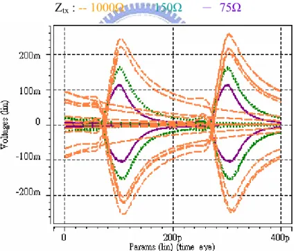
Fig. 5.4 Corner case simulation results... 43
Fig. 5.5 Layout... 44
Chapter 1
Introduction
1.1 Motivation
With the COMS technology grows in recent years, there has been a great interest in SOC design. It results in large chip size and high power consumption. In conventional chip design, the overall system efficiency depends on the performance of individual module. However, with the distance between modules increases, the module-to-module data communication bandwidth becomes an important issue of SOC design. Because the long distance communication not only decays the signal amplitude but also requires high power consumption to transmit the signal. The long distance on-chip transmission line has a large parasitic resistance, and the resistance has frequency dependence due to the skin effect. The large parasitic resistance and parasitic capacitance make the signal decay greatly. Furthermore, the power consumption of an electrical signal in SOC is governed by two components. The first component is due to leakage current and DC path between VDD and GND, known as the static power, and the second one is due to switching transient current and short circuit transient current, known as the dynamic power [1]. In conventional high speed
link design, current mode logic (CML), Positive emitter coupled logic (PECL), low
voltage differential signaling (LVDS) are mostly used. They all require a current
source to drive the communication data and the current source will increase the power consumption especially when high speed data is transmitted.
In this thesis, we will explore the pulse signaling to improve the power efficiency of long distance on-chip interconnection. The pulse signaling method is base on the fact that the AC component actually carries all the information of a digital signal and that treat the DC component as redundant. The pulse signaling transmits data by using AC coupled method and that consumes only the dynamic power. Therefore the pulse signaling would reduce the power consumption of the on-chip data communication.
Fig 1.1 On-chip long distance interconnection
Fig 1.1 shows the high speed data communication in the SOC design. The distance from driver end to receiver end is in the range of 1000um to 5000um. The long distance transmission line goes through the space between modules for saving chip area. In this way, a long distance transmission of small area overhead is required. Besides, there are also two targets to design this pulse signaling. The first is the structure must be simple and easy for implementation. The second is the circuit should operate at high speed and consume low power for SOC application. These design methodology and much more circuit details will be discussed in the following chapters. TX RX Module 1 Module 2 Module 3 Module 4 SOC
1.2 Link Components
A typical high speed link is composed of three components: a transmitter, a transmission line, and a receiver. Fig. 1.2 illustrates these components. At near end, the transmitter converts the digital data into an analog signal stream and sends that to the transmission line. During the signal propagates to the receiver, the transmission line attenuates the signal and introduces noise. In order to achieve high data rate and reduce the distortion, a transmission line with low attenuation at high frequency is required. At far end, the signal comes into the receiver. The receiver must be able to resolve small input and then amplify the incoming signal. After that, the receiver converts the signal back into binary data.
Fig. 1.2 Basic link components: the transmitter, the channel, and the receiver In this thesis, we use a pulse form signal stream which known as return-to-zero (RZ) signaling. We also use a differential structure of transmission line to reduce the common mode disturbance. At the far end, a receiver with a built-in latch is able to convert the RZ pulse back into the non-return-to-zero (NRZ) signal. Then, the converted NRZ data can be used for further receiver end usage.
1.3 Thesis Organization
This thesis describes a voltage mode pulse transmitter, a pulse receiver, and an on-chip transmission line. In chapter 2, we study the background of the high-speed serial link interface and the AC coupled communication. Some typical structures are also introduced in this chapter. In chapter 3, the on-chip pulse signaling is present. An
Transmitter Receiver
Timing
Recovery
Data out Data in
analysis of on chip pulse signaling and an on-chip differential transmission are discussed. Chapter 4 shows the design of the pulse transmitter and the pulse receiver. The experimental results and conclusions are addressed in the last two chapters. The results are also compared with some prior works.
Chapter 2
Background Study
System on chip (SOC) is the trend of today’s IC design and the high speed interface [2] [3] between chip modules is an important design issue. In the electrical industry, positive-referenced emitter-coupled logic (PECL), current mode logic (CML), and low voltage differential signaling (LVDS) are the structures commonly used in high speed link interface design. However, a current source is required to produce the IR drop that makes the signal swing. The current source not only consumes the dynamic power but also the static power. In order to save more power, AC coupled method is introduced because it only consumes the dynamic power by coupling pulse mode data. Besides, with the growing of chip size, on-chip interconnect is also getting more attention as on-chip interconnect is becoming a speed, power and reliability bottleneck for the system. In this chapter, we will briefly overview the background of high-speed serial link interface and AC coupled communication. Of course, some typical structures are also introduced in this chapter.
2.1 High Speed Link Interface
High speed links for digital systems are widely used in recent years. In the computer systems, the links usually appear in the processor to memory interfaces and
in the multiprocessor interconnections. In the computer network, the links are used in the long-haul interconnect between far apart systems and in the backplane interconnect within a switch or a router. Fig 2.1 is a generalized structure of a high speed serial link [4]. It consists of a transmitter, a transmission line, and a receiver. The transmitter side serializes the parallel data and delivers the synchronized data into the transmission line. Timing information is embedded in this serial data, which is sent over a single interconnect. The receiver side receives the serial data and recovers its timing. Then, the serial data returns to the parallel one.
Fig. 2.1 A generalized model of a serial link
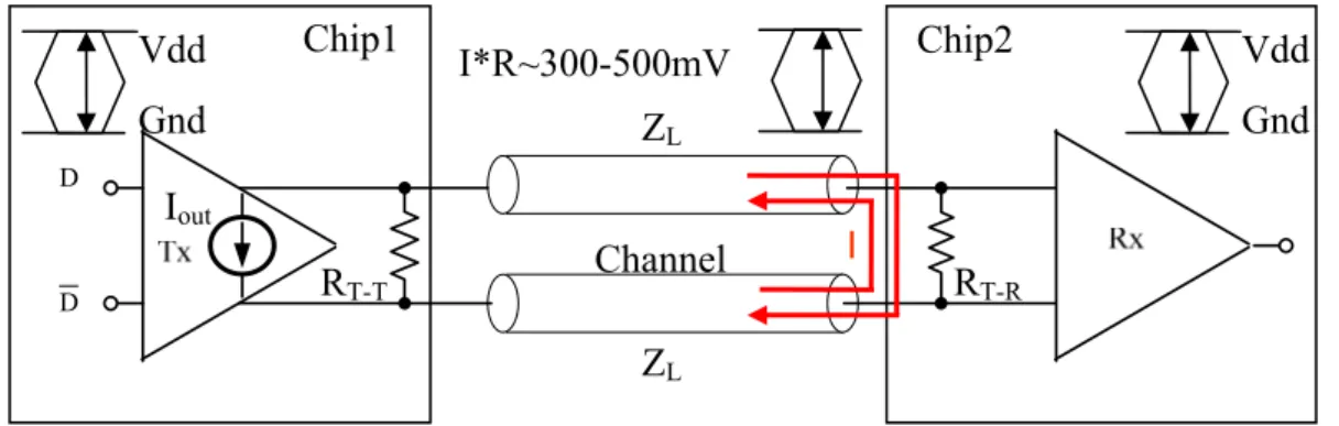
As the demand for high-speed data transmission grows, the interface between high speed integrated circuits becomes critical in achieving high performance, low power, and good noise immunity. Fig.2.2 shows the typical structure of a high speed interface. The interface usually appears in the chip-to-chip high speed data communication [5]. Three commonly used interfaces are PECL, CML, and LVDS. The signal swing provided by the interface depends on the IR drop on the termination resistance, and that decides the power consumption. The signal swing of most designs is in the range of 300mV to 500mV.
Fig. 2.2 High speed interface
Serial to Parallel Receiver N N Phase Lock Loop Clock Recovery Transmitter Parallel to Serial Transmission Line I*R~300-500mV Iout D D ZL RT-T RT-R ZL I Chip1 Channel Chip2 Gnd Vdd Gnd Vdd
2.1.1 PECL Interface
PECL [6] is developed by Motorola and originates from ECL but uses a positive power supply. The PECL is suitable for high-speed serial and parallel data links for its relatively small swing. Fig. 2.3 (a) shows the PECL output structure. It consists of a differential pair that drives source followers. The output source follower increases the switching speeds by always having a DC current flowing through it. The termination of PECL output is typically 50Ω that results in a DC current and makes Vop and Von to
be (Vdd-Vov). The PECL has low output impedance to provide good driving capability.
Fig.2.3 (b) shows the input structure of PECL. It consists of a differential current switch with high input impedance. The common mode voltage is around (Vdd-IR) to
provide enough operating headroom. Besides, decoupling between the power rails is required to reduce the power supply noise.
Fig. 2.3 (a) output structure of PECL (b) input structure of PECL
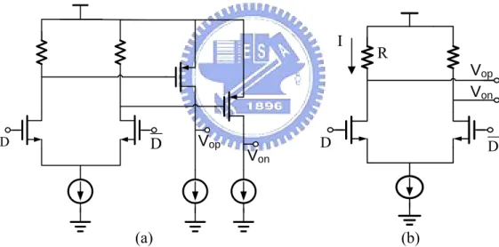
2.1.2 CML Interface
CML [6] [7] is a simple structure for high speed interface. Fig. 2.4 (a) shows the output structure of the typical CML which consists of a differential pair with 50Ω drain resistors. The signal swing is supplied by switching the current in a common-source differential pair. Assuming the current source is 8mA typically, with
the CML output connected a 50Ω pull-up to Vdd, and then the single-ended CML
output voltage swing is from Vdd to (Vdd−0.4V). That results in the CML having a
differential output swing of 800mVpp and a common mode voltage of (Vdd–0.4V). Fig.
Von Vop D D (a) (b) Vop Von D R I D
2.4 (b) shows the CML input structure which has 50Ω input impedance for easy termination. The input transistors are source followers that drive a differential-pair amplifier.
Fig. 2.4 (a) output structure of CML (b) input structure of CML
In conclusion, the signal swing provided by the CML output is small and that results in low power consumption. Besides, the termination minimizes the back reflection, thus reducing high-frequency interference. Table 2.1 [6] summarizes the electrical characteristics of a typical CML.
Table 2.1 Electrical characteristics of the CML [6]
Parameter min typ max Unit
Differential Output Voltage 640 800 1000 mVpp
Output Common Mode Voltage Vdd-0.2 V
Single-Ended Input Voltage Range Vdd–0.6 Vdd+0.2 V
Differential Input Voltage Swing 400 1200 mVpp
2.1.3 LVDS Interface
LVDS [6] [8] has several advantages that make it widely used in the telecom and network technologies. The low voltage swing leads to low power consumption and makes it attractive in most high-speed interface. Fig. 2.5 (a) shows the output structure of LVDS. The differential output impedance is typically 100Ω. A current
Von Vop 50Ω 50Ω Vdd Von Vop 50Ω 50Ω Vip Vin Vdd (a) (b)
steering transmitter provides Ib (at most 4mA) current flowing through a 100Ω
termination resistor. The signal voltage level is low which allows low supply voltage such as 2.5V. The input voltage range of the LVDS can be form 0V to 2.4V and the differential output voltage can be 400mV. These allow the input common mode voltage in the range from 0.2V to 2.2V. Fig. 2.5 (b) shows the LVDS input structure. It has on-chip 100Ω differential impedance between Vip and Vin. A level-shifter sets
the common-mode voltage to a constant value at the input. And a Schmitt trigger with hysteresis range relative to the input threshold provides a wide common-mode range. The signal is then send into the following differential amplify for receiver usage. Table 2.2 [6] summarizes the LVDS input and output electrical characteristic.
Fig. 2.5 (a) output structure of LVDS (b) input structure of LVDS Table 2.2 Electrical characteristics of LVDS [6]
Parameter Symbol Cond. min typ max Unit
Output high voltage VOH 1.475 V
Output low voltage VOL 0.925 V
Differential Output Voltage |Vod| 250 400 mV
Differential Output Variation △|Vod| 25 mV
Output Offset Voltage Vos 1.125 1.275 mV
Output Offset Variation △|Vos| 25 mV
Differential Output Impedance 80 120 Ω
Output Current togetherShort 12 mA
Output Current Short to
Gnd 40 mA
Input Voltage Range Vi 0 2.4 V
Vo Vip Vin (a) (b) Vocm Von Vop Ib Ib Vin Vip Vin Vip
Differential Input Voltage |Vid| 100 mV
Input Common-Mode Current VInput
os=1.2V 350 uA
Hysteresis Threshold 70 mV
Differential Input Impedance Rin 85 100 115 Ω
2.2 AC Coupled Communication
2.2.1 AC coupled communication
The AC coupled interface [9] [10] [11] uses pulse signal to transmit data. It has the advantage of less power consumption. The AC component actually carries all the information of a digital signal and thus an AC coupled voltage mode driver can be used to improve the power consumption because only the dynamic power is presented. Coupling capacitor acts like a high-pass filter that passes the AC component of the data to the data bus.
(a)
(b)
Fig. 2.6 (a) AC coupled communication [12] (b) pulse waveform in transmission line GND VDD 300mV GND VDD 1ns
Fig. 2.6 (a) shows the AC coupled communication [12]. The transmitter (in chip 1) and the receiver (in chip 4) are connected to the data bus through an on-chip
coupling capacitor Cc at pad. Both end of the data bus are terminated by the
impedance matching resistors Z0 with termination voltage Vterm. Fig 2.6 (b) indicates
the waveform of the pulse communication. The input full swing data sequence is coupled to pulse form by the capacitor at the transmitter output. The amplitude of the pulse signal is roughly 300mV at the data rate of 1Gbps. The receiver obtains the pulse mode data through the coupling capacitor and then amplifies the decayed signal to full swing.
2.2.2 Typical pulse transmitter / receiver
Pulse signaling [15] [16] typically uses a voltage-mode transmitter [17] as shown in Fig. 2.8. The transmitter output is connect to a coupling capacitor and then to the transmission line. Return impedance matching at the transmitter output is provided by the termination resistor. The voltage mode transmitter provides a full swing as well as high edge rate output to drive the transmission line. Without DC current consumption, the voltage mode transmitter consumes less power than a current mode transmitter.
Fig. 2.7 voltage mode transmitter
Fig 2.9 (a) shows the pulse receiver proposed by Jongsun Kim in 2005 [12]. The enable function is design for saving power if the circuit is in the off mode. The equivalent circuit with enable on is shown in Fig. 2.9 (b). The cross-couple structure
not only senses the pulse signal but also provides the latch function to transform the pulse signal into NRZ data.
(a)
(b)
Fig. 2.8 (a) pulse receiver (b) equivalent circuit with enable on
Fig 2.10 shows another low swing pulse receiver proposed by Lei Luo in 2006 [14]. The diode connected feedback M1~M4 limits the swing at the out of inverter. Meanwhile, M5 also M6 provide a weak but constant feedback to stabilize the bias voltage, making it less sensitive to the input pulses. Source couple logic M7~M9 further amplifies the pulse and cross-coupled M11 & M12 serves as a clock free latch to recover NRZ data. In addition, a clamping device M10 limits the swing of long 1’s or 0’s and enable latch operation for short pulse which improves the latch bandwidth. The structure is able to receive pulse of the swing as small as 120mVpp.
Chapter 3
On-Chip Pulse Signaling
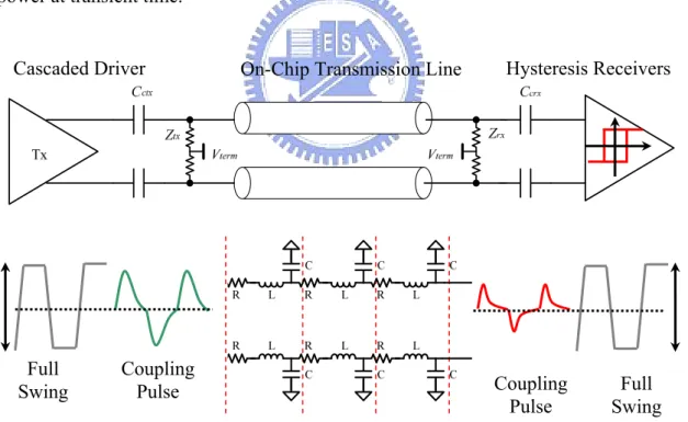
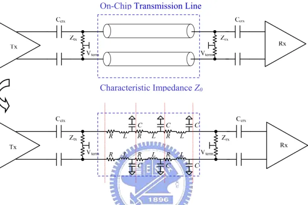
This chapter introduces the on-chip pulse signaling. It includes the pulse signaling mathematic model and the geometry of the on-chip differential transmission line. On-chip transmission line [18] [19] has a large parasitic resistance. The resistance is frequency dependent due to the skin effect. The large parasitic resistance and parasitic capacitance make the signal decay greatly [20]. Thus, a wide line is required for long distance and high-speed signal transmission. However, the wider line and space between lines require more layout area. That will increase the costs of the SOC. That is why a low cost and large bandwidth transmission line is desired. Moreover, the characteristic impedance of transmission line is also discussed in this chapter. Theoretically, impedance matching among the transmitter end, the receiver end, and the transmission line is required. That can prevent the signal from reflecting in the transmission line. In this thesis, a single end termination is implemented. The single termination method can guarantee the signal reflects at most once. The designed termination impedance is 75Ω for less attenuation. The width, space, and length of the transmission line are 2.3um, 1.5um, and 5000um respectively. The transmission is implemented with Metal 6 and Metal 5 of TSMC RF013um technology.
3.1 Pulse Signaling Scheme
Fig. 3.1 shows the on-chip pulse signaling scheme. The transmitter and the receiver are coupled to the on-chip transmission line through the coupling capacitor
Cctx and Ccrx. Transmitter and receiver ends of the data bus are terminated by the
impedance Ztx and Zrx respectively with the terminated voltage Vterm. Furthermore, the
transmission line acts like the distributed RLC that decays the transmitted data. The coupling capacitor makes it a high-pass filter that transmits the transient part of the input data. The DC component is blocked. The pulse signaling method is base on the fact that the AC component actually carries all the information of a digital signal. The DC component is treated as redundant. In this way, the pulse data acts as return to
zero signaling (RZ). In contrast to non-return to zero (NRZ) signaling, pulse signaling
has been used to reduce the power consumption by only dissipating the dynamic power at transient time.
Fig. 3.1 Pulse signaling scheme
In Fig 3.1, full swing data is fed into the transmitter input. The transmitted data in the transmission line is a pulse coupled by the coupling capacitor at the transmitter output. After long distance of transmission, the received pulse is coupled to the
On-Chip Transmission Line
Cascaded Driver Hysteresis Receivers
Full Swing Coupling Pulse Coupling Pulse Full Swing
hysteresis receiver by the coupling capacitor as well. The receiver end biases the pulse to the DC common mode voltage of the hysteresis receiver. After that, the hysteresis receiver transfers the RZ pulse data to NRZ full swing data.
3.2 On-chip pulse signaling analysis
Fig 3.2 (a) defines the on-chip pulse signaling model and Fig 3.2 (b) is the corresponding transient response of the transmitter. Let Zt be the characteristic
impedance of the transmission line, Ztx and Zrx the termination resistances at the
transmitter end and receiver end, Cctx and Crtx the coupling capacitors, Cd and Cg the
parasitic capacitance at transmitter output and receiver input respectively. The transfer function from transmitter output (A) to near end transmission line (B) is
tx t ctx tx t AB tx t tx t d ctx ctx 1 +(Z //Z ) sC (Z //Z ) H (s)= 1 1 1 + +(Z //Z ) +(Z //Z ) sC sC sC × . tx t ctx d tx t ctx d ctx d (Z //Z )C C s = (Z //Z )C C s +(C +C ) (3.1)
Equation (3.1) shows the high-pass characteristic and that HAB(s) is dominated by
tx t ctx d
(Z //Z )C C in high frequency. In other words, large coupling capacitor and
termination resistance are better for transferring the pulse signal. Moreover, the transfer function from the near end (B) to the far end C) is
. crx g rx ch crx g BC crx g ch ch rx ch crx g C +C 1 ( //Z // ) sC sC C H (s)= C +C 1 R + sL +( //Z // ) sC sC C
Because Ccrx and Cg are typically in the order of femto-farad, (Ccrx+Cg)/sCcrxCg <<1
and the transfer function becomes
. ch rx BC ch ch ch rx 1 ( ) 1 sC + Z H (s) 1 R + sL +( ) 1 sC + Z ≈ (3.2)
Equation (3.2) shows the channel bandwidth is roughly 1/RchCch. The parasitic resistance and capacitance of the transmission line limits the channel bandwidth. Furthermore, the transfer function from the far end (C) to the receiver input (D) is
g CD crx g 1 sC H (s)= 1 1 + sC sC crx crx g C = C +C . 2 ch ch ch ch ch ch rx rx 1 = L R C L s +(R C + )s +( +1) Z Z (3.3)
Equation (3.3) shows that the receiver pulse is proportional to the value of coupling capacitor (Ccrx ).
Fig. 3.2 (a) On-chip pulse signaling model (b) Transient response of the transmitter Node A Node B Vp Vterm Vdd tr td Pulse Width≒ tr + td (a) A B C D Z (b)
The step response is important in analyzing the pulse signaling. A step input voltage at node A results in a transient on node C. Transforming a square wave into a short triangular pulse wave on the transmission line. The amplitude (Vp) becomes
p eff c V = R I A tx t c dV = (Z //Z )C dt (3.4)
and the voltage value at node B is
eff eff t -R C B p term V (t)= V e +V . t -t p term = V e +V (3.5) Where R = (Z //Z ) , 1/C = 1/C +1/C , C = C C /(C +C ) eff tx t eff ctx d eff ctx d ctx d andt = R C . eff eff
Equation (3.4) shows that the amplitude of the pulse is proportional to three parts: the equivalent value of the termination resistance parallel to the characteristic resistance, coupling capacitance, and the slew rate at the transmitter output. As illustrated in Fig 3.2 (b), the transmitter needs to provide a large amplitude value of pulse signal for the decay in the transmission line. However, after the transition time, the transmitted waveform becomes steady and the coupling pulse decays according to the RC time constant. The pulse width roughly equals to the rise time during the pulse transition plus the RC decay time. If the amplitude is too large, it creates the pulse tail and that leads to the ISI effect. This ISI effect not only limits the communication speed but also increases the jitter at the receiver end. In other words, large coupling capacitance and large termination resistance are good for transferring the pulse signal but that also create the ISI issue. In this thesis, we bring up an equalization method to reduce the ISI effect. The details will be discussed in the chapter 4.
3.3 On-Chip Differential Transmission Line
3.3.1 Mode of Transmission Line
As the wire cross-section dimension becomes smaller and smaller due to the technology scaling down and the wire length increases due to growing in chip size, not only the capacitance but also the resistance of the wire becomes significant. Besides, the wire inductance becomes important as well for the faster circuit operating speed and relatively lower resistance from the new technology. The current distribution inside the conductor changes as the frequency increases. This change is called the skin effect and that results in variations of resistance and inductance value.
Fig. 3.3 shows the on-chip transmission line. When ωL is comparable to R then the
wire should be modeled as a distributed RLC network. The frequency dependent behavior of the transmission line decays the pulse signal in the channel and makes the amplitude too small to receive at the far end.
Fig. 3.3 On-chip transmission line as a distributed RLC transmission line
Fig. 3.4 (a) shows the proposed on-chip differential transmission line which is fabricated by TSMC 0.13µm RF technology. A co-planar transmission line is placed in Metal 6. Metal 5 below is reserved for ground shielding. A micro-strip structure is used in GSGSG placing, ‘S’ for signal and ‘G’ for ground. The ground path is not only
for signal return but also for the ground shielding. The transmission line model is analyzed and extracted to build the distributed RLC parameters by PTM [21]. Fig. 3.4 (b) illustrates the cross section of the differential transmission line. The total length (l)
of the line is 5mm. The line width (w) is 2.3µm and line-to-line space (s) is 1.5µm.
On-Chip Transmission Line
Fig. 3.4 (a) Micro-strip structure and the parasitic effect (b) Cross section of the on-chip transmission line
3.3.2 Geometry Analysis of Transmission Line
Table 3.1 shows the data obtained from PTM. The dimension is obtained form the TSMC 013RF technology document. The thickness (t) of Metal 6 is 0.37µm, the
height (h) from Metal 5 to Metal 6 is 0.45µm, and the dielectric constant (k) is 3.9.
The total parasitic RLC value divided by the total length of the transmission line obtains the parasitic RLC in unit length. The distributed parasitic parameters are
Rul=25.85Ω/mm, Lul=1.74nH/mm, and Cul=306.70 fF/mm.
Table 3.1 Parasitic RLC of the on-chip transmission line
Dimension RLC ( 5mm ) RLC ( /mm ) w = 2.3µm s = 1.5µm l = 5000µm t = 0.37µm h = 0.45µm k = 3.9 R = 129.259Ω L = 8.728nH M12 = 6.876 nH M13 = 6.183 nH M14 = 5.779nH K12 = 0.787 K13 = 0.708 K14 = 0.662 Rul =25.8518 Ω/mm Lul =1.7456 nH/mm Cg =251.088 fF/mm Cc =27.807 fF/mm Cul =306.702 fF/mm k h s w Gnd l S G S G G t
Ccouple Ccouple Ccoupl Ccouple
S G S G G Gnd Cground Cground Metal 6 Metal 5 (a) (b)
Cc = 1255.44 fF Cg = 139.035 fF Ct = 1533.51 fF
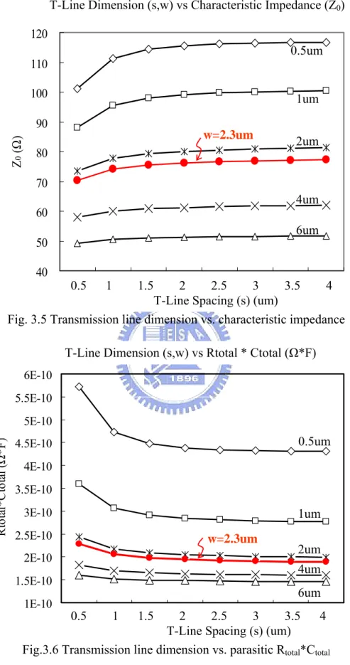
According to the data mentioned above, the characteristic impeadance (Z0) of the transmission line is 0 ul ul ul R j L Z j C ω ω + = . ul ul L C ≅ (3.6)
The characteristic impedance of the designed differential transmission is 75Ω. Fig. 3.5 shows the relationship between the dimension of the transmission line versus its characteristic impedance. Fig. 3.6 also illustrates the relationship between the dimension of transmission line versus its parasitic Rtotal*Ctotal which is equivalent to the bandwidth of the line. These two figures tell that smaller width as well as spacing results in larger characteristic impedance value. From (3.1), we know that it is good for coupling pulse because the high pass characteristic. However, small width as well as spacing results in large parasitic Rtotal*Ctotal which makes the signal decay greatly.
On the contrary, wider width and spacing of the transmission line results in better frequency performance of the transmission line. But it also requires more layout area which increases the cost of SOC. The design of w=3.2µm and s=1.5µm meets the characteristic impedance of 75Ω. And there are three main reasons for this value. Firstly, 75Ω of characteristic impedance makes the parasitic Rtotal*Ctotal < 2E-10
(Ω*F) which decay the signal roughly 18dB. Secondly, 75Ω is close to 77Ω which theoretically causes minimum attenuation. Thirdly, the values of the width and spacing reduce the layout area as well as the costs.
Fig. 3.5 Transmission line dimension vs. characteristic impedance
Fig.3.6 Transmission line dimension vs. parasitic Rtotal*Ctotal
40 50 60 70 80 90 100 110 120
5.0E-07 1.0E-06 1.5E-06 2.0E-06 2.5E-06 3.0E-06 3.5E-06 4.0E-06 T-Line Spacing (m) Z 0 ( Ω ) 0.5um 1um 2um 6um 4um w=2.3um 0.5 1 1.5 2 2.5 3 3.5 4 T-Line Spacing (s) (um)
T-Line Dimension (s,w) vs Characteristic Impedance (Z0)
1E-10 1.5E-10 2E-10 2.5E-10 3E-10 3.5E-10 4E-10 4.5E-10 5E-10 5.5E-10 6E-10
5.0E-07 1.0E-06 1.5E-06 2.0E-06 2.5E-06 3.0E-06 3.5E-06 4.0E-06 T-Line Spacing (m) R to ta l* C to ta l ( Ω *F ) 0.5um 1um 2um 6um 4um w=2.3um 0.5 1 1.5 2 2.5 3 3.5 4 T-Line Spacing (s) (um)
Chapter 4
5Gpbs Pulse Transmitter/Receiver
Circuit Design
This chapter introduces the pulse transmitter and pulse receiver operating at 5Gbps. At the near end, we increase the termination resistance for better high-pass characteristics. The equalization circuit built in the transmitter also cuts the pulse tail and depresses the ISI effect as discussed in chapter 3.2. At the far end, three functions are required: biasing the received pulse to the common mode voltage of the receiver, amplifying the received pulse amplitude, and transferring the RZ pulse to NRZ data. These functions are implemented by a self-bias and equalization circuit, an inductive peaking amplifier, and a non-clock latch. The following sections will discuss these circuits and their design methodology.
4.1 Pulse Transmitter Circuit
4.1.1 Voltage Mode Transmitter
In high-speed serial link design, the near end typically uses a current mode driver as discussed in Chapter 2, but the pulse signaling must use a voltage mode driver as
shown in Fig. 4.2 (a). The transmitter output is connect to a coupling capacitor (Cctx) and then to the on-chip transmission line. Return impedance matching at the transmitter output is provided by the termination resistances (Ztx). There are two advantages to use a voltage mode transmitter rather than a current mode one. First, the voltage mode transmitter is much easier to drive the transmission line of high input impedance. Secondly, the transmission line loss as well as the high frequency pass-band characteristic of the transmission line requires a full swing and high edge rate transmitter output. The voltage mode transmitter is quite suit for that. Besides, the voltage mode transmitter consumes dynamic power and has no DC current component on the transmission line. That results in less power consumption than a current mode
transmitter. Although dynamic supply current will introduce the synchronous
switching noise (SSN), we can add slew rate control circuit or add decoupling
capacitor between power rails to reduce the effect.
Fig. 4.1 Output pulse signal at transmitter with different termination resistance As discussed in Chapter 3, the high pass characteristic of the transmitter passes the transient part of the input data and blocks the DC signal component. Equation (3.1) and (3.4) also implies that we can use a large termination resistor to generate the better high-pass characteristics. Fig 4.1 shows different values of the termination resistors and the corresponding pulse signals. The larger value of the termination
resistance is, the larger amplitude of the pulse signal will be delivered. The trade off is that the large termination resistance will introduce a pulse tail within a bit time. This tail not only limits the maximum transmission speed but also increases the ISI effect. In section 4.1.2, we introduce an equalization method to solve this problem.
4.1.2 The Proposed De-emphasis Circuit
Fig. 4.2 (b) shows a de-emphasis structure for the equalization. The structure consists of a buffer and a coupling de-emphasis capacitor (Ccde) connected to the
differential node of the transmitter output. The main idea is to use the structure to generate a complementary pulse and add the complementary pulse to the original signal. In this way, the output pulse signal at the near end can be describes as
.
y(n)= x(n)+ kx'(n) (4.1)
Fig. 4.2 Voltage mode transmitter (a) without de-emphasis (b) with de-emphasis
Cctx Ninv Ztx Cctx Ccde Ninv Ztx
Where x(n) is a full swing data at the last stage of the transmitter, x(n)’ is the
complement of x(n), and k is a weighting factor which depends on the delay of the
buffer and the value of the de-emphasis capacitor. Fig. 4.3 illustrates the circuit behavior of the transmitter. Take the positive terminal for example, The Vop is a positive full swing data at the transmitter output and the x is the coupling pulse. The Von is negative as contrast to Vop. The buffer at negative terminal delays the full swing
data. And then, the de-emphasis capacitor adds the complement pulse x’ to the
positive terminal to remove the pulse tail. The de-emphasis circuit can reduce the ISI effect and increase the maximum transmission speed.
Fig. 4.3 Coupled pulse signal with de-emphasis circuit
4.1.3 Pulse Transmitter Design Flow and simulation results
Fig. 4.4 Pulse transmitter Td Data Coupling Pulse Vop Von Pulse x x’ y
Fig. 4.4 shows the pulse transmitter circuit which consists of a series of cascaded inverters as the driver (last stage of size Ninv), a de-emphasis buffer and the coupling capacitors. The driver uses n cascaded inverters and each one of them is larger than
the preceding stage by a width factor f. Then, the relationship between the output
loading capacitor (CL) and the driver input capacitance (Cgi) can model to be
. n L L gi gi C C f = n = log logf C C ⇒ (4.2)
Let the equivalent pull-up resistance (Rpu) and the equivalent pull-down resistance (Rpd) of the inverter are equal. The time constant (τ ) of the first stage is ( Rpu+ Rpd)Cgi/2 and total delay (td) becomes fτ (log(CL/Cgi)/logf) . Take dtd/df=0 can
obtain the best choice of f (usually take f=e≈ 2~3). And then, the loading of the driver including de-emphasis circuit becomes
CL=fnCgi=Cctx+Cgbufferr . (4.3) Let the gate capacitance of the buffer is x factor larger than Cgi (Cgbufferr= xCgi), then the coupling capacitor can be calculated
Cctx=fnCgi-Cgbufferr=(fn-x) Cgi (4.4)
Fig. 4.5 Pulse Transmitter design flowchart Slew Rate (or Power Budget )
Decide Ninv
Rising Time of Input Data Decide Td Equation (4.4) Decide Cctx Equation (3.1) Decide Ztx Decide Ccde
Besides, from equation (3.1) the proper termination resistance (Ztx) can be decided. Fig. 4.5 shows the design flowchart of the transmitter. The buffer delay (Td) depends on the process and we can obtain the best result by fine tuning the de-couple capacitor (Ccde). Fig. 4.6 is the simulation of the pulse signal at the transmitter output with de-emphasis circuit included. The diamond eye shows the de-emphasis circuit cuts the pulse tail and reduces the ISI effect in one data period (200ps). The voltage swing at the near end is 400mVpp with using a coupling capacitor of 280fF and a
de-emphasis capacitor of 140fF.
Fig. 4.6 Simulation of coupled pulse signal with de-emphasis
4.2 Pulse Receiver Circuit
A pulse receiver is used to transfer RZ pulse into NRZ data. Since the coupling capacitor blocks the DC signal, the receiver end needs to bias, amplify, and then convert the RZ pulse signal into NRZ data. Fig. 4.7 illustrates the receiver end circuit blocks. Because the incoming signal at far end is a short pulse with amplitude smaller then 50mV, a self-bias and equalization circuit is used to bias the pulse to the receiver common-mode voltage. A differential pre-amplify is then connected to amplify the small pulse. After that, a non-clock latch with hysteresis has the ability to filter out the incoming noise from imperfect termination and common-mode disturbances such as
--- Without de-emphasis
ground bounce. The recovered NRZ data can then fed to a traditional clock and data recovery circuit to generate receiver end clock and re-sample the NRZ data.
Fig. 4.7 Receiver end circuit block
4.2.1 Receiver End Termination
To minimize reflections, either or both side of the transmission line should be impedance matched. In this thesis, a receiver end termination is implemented. Terminating at the receiver side reduces reflections and allows the transmitter side to have high-pass behavior as a transmitted pulse encounters the high impedance transmitter. There is reflection noise at the far end transmission line due to the forward reflection at the un-terminated near end transmission line. This forward reflection noise is absorbed by the far end termination resistor and thus no further backward reflection noise shown at the near end termination line. Fig. 4.8 illustrates the receiver end termination. The Ceq is the equivalent capacitance of the receiver end coupling capacitor (Ccrx) in serial with the receiver end gate capacitance (Cg). In general, a node capacitance of a digital circuit is roughly 20fF. The Ccrx in our design is 240fF. Thus, the equivalent capacitance Ceq=CcrxCg/(Ccrx+Cg) ≈ 20fF. In other words, the input impedance at receiver end becomes
Driver End 200mV Pulse Non-Clock Latch With Hysteresis Self-Bias & Equalization Circuit A Full Swing NRZ Data Receiver End <50mV Pulse 5mm Pre-amplifier >200mV Pulse A
. rx eq rx rx rx rx eq eq rx eq rx eq 1 R sC R R 1 Z = R // = = = 1 sC R + 1+ sRC 1+ 2 fR C j sC π (4.5)
Where the Rrx is the receiver end termination resistance which is equal to the characteristic resistance of the transmission line (75Ω) and the magnitude is
. rx rx 2 2 rx rx eq R Z = R 1 +(2 fR C )π ≈ (4.6)
Equation (4.6) tells that Zrx is equal to Rrx in low frequency range. According to TSMC 013RF technology, the maximum rise time (Tr) of a single inverter is roughly 40ps over 1.2V power rails. This means that the edge rate of a pulse signal is f ≈ 0.3/ Tr =9GHz. The termination resistance in our design matches well over the frequency
range including at the data rate (5Gbps) as well as at the signal edge rate (9GHz).
Fig. 4.8 Receiver end termination scheme
Fig. 4.9 shows the simulation results of the impedance matching at the receiver end. Though at high frequencies, the parasitic gate capacitance and the coupling capacitor reduce Zrx, the impedance still matches well across a wide frequency range.
A B C D Z Zrx Ceq
Fig. 4.9 Impedance looking from the transmission line to receiver
4.2.2 Self-Bias and Equalization Circuit
Fig. 4.10 shows the self-bias and equalization circuit. The circuit not only automatically generates the receiver end common-mode voltage but also reduces the low frequency component of the incoming pulse signal. As illustrated in the dash line area, an inverter with input connected to output generates the Vdd/2 common mode
voltage. The common mode voltage is then connected to the receiver differential ends through two transmission gates. The size of the self-bias inverter in our design is the same as the pre-amplifier in the next stage for the matching consideration. Besides, the transmission line has a low-pass response which is due to the skin effect. The low-pass response results in a long tail on the pulse signal. If there is no equalization, the tail will cause the ISI effect and reduce the timing margin at the receiver end. In Fig. 4.10, the dotted line area indicates the equalization circuit which consists of an inverter and a de-emphasis capacitor. The circuit de-emphasizes the low frequency components by generating a small complementary pulse and adding the complementary pulse to the original signal. The output pulse signal of the self-bias and equalization circuit can be express in
.
y(n)= x(n)+ kx'(n)
Impedance Matching (Zrx)
Impedance
Fig. 4.10 Receiver end: Self-bias and equalization circuit
Where x(n) is the pulse signal at the output of the self-bias and equalization circuit, x(n)’ is the complement of x(n), and k is the weighting factor which depends on the
delay of the inverter and the size of the de-emphasis capacitor. Fig. 4.11 shows the behavior of the circuitwith using a coupling capacitor of 240fF and a de-emphasis capacitor of 5fF.
Fig. 4.11 Pulse waveform after equalization circuit
4.2.3 Inductive Peaking Amplifier
An inductive peaking amplifier is composed of parallel inverters as the gain stage with its output connected to an inductive peaking cell as shown in Fig 4.12. The main idea of the circuit is to use the inverter gain for signal amplification and the
Self-bias And Equalization Circuit Pre-amplify Stage Non-Clock Latch With Hysteresis x x’ y x x’ y Td
inductive peaking for improving the high-frequency performance. Fig. 4.13 (a) shows the inductive peaking cell. Each inductive peaking cell consists of a small size inverter and a resistor. The inverter is configured as diode connected by a resistor which is implemented with a transmission gate as illustrated in Fig 4.12. The diode connected inductive peaking cell lowers the output resistance of the inverter and so does the gain. As a result, the 3dB frequency increases as the output resistance decreases. At low frequency, the output resistance is roughly 1/gm, while it roughly
equals to the resistance of a transmission gate at high frequency. It is intended to design the resistance of a transmission gate to be larger than 1/gm, so it increases gain
and extends bandwidth at high frequency.
Fig. 4.12 Receiver end: Inductive peaking amplifier
In other words, the attached inductive peaking cell at the output of the inverter sacrifices gain but obtains bandwidth to enhance the high-frequency performance. Moreover, as illustrated in Fig. 4.13 (b), this circuit not only amplifies the high frequency component but also depresses the low frequency pulse tail. A lightly transition overshoot due to the inductive peaking results in good performance in the high frequency part. The pulse signal is amplified larger than 200mV and fed into the hysteresis latch. Self-bias And Equalization Circuit Non-Clock Latch With Hysteresis Pre-amplify With Inductive Peaking
Fig. 4.13 (a) Inductive peaking cell (b) Pulse waveform after inductive peaking amplify Although the inductive peaking cell doesn’t have any actual inductor inside, the parasitic capacitance of inverter (Cgdp, Cgdn) combining the resistor generates a high frequency zero that improves the high frequency performance. The frequency response is like adding an inductor. This broadband technique is so called the inductive peaking. Fig. 4.14 shows the gain-bandwidth plot of the inductive peaking amplifier. The 3dB bandwidth extends from 3.88GHz to 11.3GHz after the inductive peaking cell is used. The receiver sensitivity depends on the equalization as well as the peaking ability of the amplify stage.
Fig. 4.14 Gain-Bandwidth plot of inductive peaking amplifier
No Inductive Peaking f3db=3.88GHz Inductive Peaking f3db=11.3GHz i O Cgdp Cgdn R 200ps <50mV Pulse >200mV Pulse (a) (b)
4.2.4 Non-clock latch with hysteresis
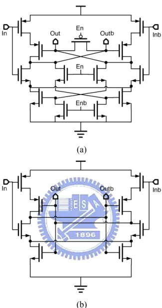
The non-clock latch transforms the RZ pulse into NRZ data. So that the recovered NRZ data can then be fed to a traditional clock and data recovery circuit to generate the receiver end clock to re-sample the NRZ data. Fig 4.15 illustrates the non-clock latch structure established from four inverters and Fig. 4.16 shows its schematic. Via and Vib are the differential inputs and Voa and Vob are their corresponding differential outputs. Two small size inverters are connected back to back at the differential output to generate the hysteresis range.
Fig. 4.15 Receiver end: Non-clock latch with hysteresis
As demonstrated in Fig. 4.16 and Fig. 4.17, when the input Via goes from logic high (H) to the trigger point (Vtrp-), the corresponding output Voa will goes from logic low (L) to the threshold point (Vth). If we let βp= μpC (W/L)ox pmin , βn=
nCox
μ (W/L)nmin (where µ is the mobility of transistor, Cox is the oxide capacitance, and (W/L) is the aspect ratio of the transistor). Then, the total current flows through
the node Voa becomes
px py nx ny I + I = I + I - 2 dd 2 p dd TRP tp p dd tp V 1 1 X [(V -V )-V ] + Y [(V - )-V ] 2 β 2 β 2 = . - 2 dd 2 n TRP tn n tn V 1 1 = X (V -V ) + Y ( -V ) 2 β 2 β 2 (4.7) Self-bias And Equalization Circuit Pre-amplify Stage Non-Clock Latch With Hysteresis
Where X is size of the input inverter and Y is the size of the back to back inverter pair.
With the following replacements:
1 p B = Xβ ,B = X2 βn ,B = (V -V ) ,3 dd tp B = V ,4 tn 2 2 dd dd 5 p dd tp n tn V V B = (Y [(V - )-V ] +Y ( -V ) ) 2 2 β β , 2 2 1 1 2 A = (B - B ),A = (B + B )(B B - B B )-(B - B )(B B + B B ),2 l 2 2 4 1 3 1 2 2 4 1 3 . 2 2 3 1 3 2 4 5 A = (B B ) -(B B ) - B (4.7) becomes . - 2 -1 TRP 2 TRP 3 A (V ) + A (V )+ A = 0
The trigger point can be solved
[
]
.
TRP-V = roots( A1 , A2 , A3 ) (4.8)
Fig. 4.16 Non-clock latch with hysteresis circuit
Take TSMC 013RF technology for example, for X = 3, Y = 1 , V = 1.2(V) , dd
2 p= 1.5166e - 3 (A/V ) β , 2 n= 1.8198e - 3 (A/V ) β , V = 403.817e - 3 (V) , and tp tn
V = 403.596e - 3(V) , we can obtain the trigger point (VTRP-) of 0.5578V. The proper design of X and Y values makes the hysteresis range to filter out the incoming noise and the interference.
Voa Vob Via Vib H
→
VTRP- L→
Vth X YFig. 4.17 Simulation of non-clock latch with hysteresis circuit
Fig. 4.18 Jitter from the receiver Data Ideal Pulse Over Peaking Vp Vp Vp Vp Jitter Trigger Point Of Latch VTRP+ VTRP -Voa Via VOL VOH
Inductive peaking amplifier may over peak the pulse signal for some corner cases especially in the SS corner. This is because the resistance of the peaking cell will change and results in different peak ability. Fig 4.18 illustrates the circuit behavior of the pulse receiver. This over peaking behavior will contribute some jitter at the receiver end. However, the hysteresis range of the latch can solve this problem. As long as the peaking amplitude is smaller than the hysteresis range, the latch can ignore the over peaking.
Chapter 5
Experiment
One prototype chip was designed in TSMC 013RF technology to verify the research ideas presented in previous chapters. The prototype chip contains a voltage mode transmitter, a 5mm long differential transmission line, and a pulse receiver. Besides, in order to drive the large parasitic capacitance on the output pad, open drain output drivers are used for the receiver differential output. In this way, the 5Gbps high-speed data can be measured on the oscilloscope. The simulated peak-to-peak jitter at the pulse receiver output is 43.7ps. The die size of the chip is 884×644µm2 with the power consumption of 3.4mW at the transmitter end and 3.2mW at the receiver end.
5.1 Simulation Setup
A test chip is implemented in TSMC 013µm RF technology. The building block of the system is shown in Fig. 5.1. We apply a sequence of random data to the input of the voltage mode pulse transmitter. The data are transported in pulse mode through the coupling capacitor (Cctx) to the on-chip transmission line. As illustrated in Fig
Metal 5 as the shielding ground. In addition, the differential structure of the transmission line also has the shielding grounds in the arrangement of ‘GSGSG’
between signal paths. The differential scheme has higher immunity to reject noise and the shielding ground reduces the environmental interference as well as the crosstalk between signal lines. At far end, the pulse data is coupled to the hysteresis receiver by the coupling capacitors (Ccrx). The receiver then transforms RZ pulses signal to NRZ
data.
Fig. 5.1 System Architecture
In order to drive a large parasitic capacitance of an output pad, open drain output drivers are used for receiver differential output as shown in Fig.5.2. The package of the chip is modeled as a pad (C=1pF) connected to a pin (C=1pF) on the printed circuit board through a pounding wire (L=2nH). Thus, the open drain circuit will
introduce a current (Ics) from the outside-chip power supply. The current goes through the impedance matching resistor (50Ω) and drives the large parasitic capacitance on
O O Ccr Rx Zrx=75Ω Vterm D D Tx Cct Ztx Vterm Cctx=280fF Cde=140fF Ccrx=240fF Cde=5fF Ztx=1000Ω
5mm on-chip differential line with shielding ground
5Gpbs eye
G S G S G
Cross-section of T-Line
the package. One oscilloscope with 100nF bypass capacitor connected to the pin is used to probe the signal at the chip output. Therefore, we can observe the eye diagram on the oscilloscope.
Fig. 5.2 Common source circuit connects to pad for output signal measurement
5.2 Experiment and Results
Fig. 5.3 shows the system simulation results. The transmitter end sends the differential pulse signal with an amplitude of 400mVpp. After a 5mm long on-chip
transmission line, the pulse amplitude decays to 50mVpp at the receiver front end. The
pre-amplifier stage amplifies the pulse amplitude to 400mVpp and fed it to the
hysteresis latch. The latch then turns the RZ pulse signal into the full swing NRZ data. After the open drain circuit as discussed in section 5.1, the oscilloscope can measure the received data with a swing of 240mVpp. Fig. 5.4 shows the eye diagrams at the
receiver output in different process corners. The eye diagram of the receiver shows the peak-to-peak jitter is 43.7ps (0.218UI) in the TT case. The worse case takes place in SS corner and the jitter is 82.7ps (0.413UI).
Vpp= Ics x 50 PAD Buffer Receiver 50Ω Oscilloscope 100nF PIN 2nH 1pF di v L dt = Inside Chip
Common Source (Open Drain)
Connect To PAD Ics
Fig. 5.3 System simulation results
The proposed on-chip pulse signaling is implemented by National Chip Implement Center (CIC) in TSMC 013RF technology. The core area is 584.7µm×411.5µm including a transmitter of 96.1µm×57.8µm, a receiver of 80.1µm×52.1µm, and a 5mm long on-chip transmission line. The total area is 884µm×644µm as shown in Fig 5.5. Table 5.1 lists the chip summary. The power consumption of the transmitter is 3.4mW, and it is 3.2mW for the receiver at the data rate of 5Gbps. 400mVpp ~240mV Full Swing Rx after Pre-Amp 400mVpp 50mVpp Input Data Tx Pulse Rx Pulse 400mVpp ~240mV Full Swing Latch Oscilloscope
Fig. 5.4 Corner simulation results Table 5.1 Specification Table
Item Specification (unit)
Process TSMC 0.13µm RF
Supply Voltage 1.2V
Data Rate 5Gb/s / channel (at 2.5GHz)
BER <10-12
Coupling Caps Tx (280+140)fF ; Rx (240+5)fF
Link 5mm and 75Ω on chip micro-strip line
Jitter of receiver data (pk-to-pk) 43.7ps (0.218UI)
Transmitter End Layout Area 57µm x96µm
Receiver End Layout Area 52µm x78µm
Core Layout Area 884µm x644µm
Pulse Driver 3.402mW
Power dissipation Pulse Receiver 3.213mW
Total 6.615mW TT 43.7ps (0.218UI) FF 29.6ps (0.148UI) FS 52.5ps (0.262UI) SF 49.7ps (0.248UI) SS 82.7ps (0.413UI)
Fig. 5.5 Layout
Table 5.2 lists the comparison of the pulse signaling and other on-chip communications. Our work uses TSMC 013RF technology to implement an on-chip 5Gbps pulse signaling. The total communication distance is 5mm with a differential transmission line of width in 2.3µm and line-to-line spacing in 1.5µm. The line consumes small area overhead as compares to other on-chip differential lines [22] [23]. Compared to the twisted differential wire method [24], our work uses a wider width as well as the wider line-to-line space. But the twisted differential wire method has only 40mVpp voltage swing at the far end. However, our work has full swing data
at receiver output and that can be used for further receiver end usage. The power consumption of the transmitter in our work is 0.68pJ/bit and the total power is 1.32pJ/bit. Our work is the lowest in power consumption.
5mm On-Chip Differential Transmission Line Tx Rx gndtx vip vddtx vddrx vpon vpop vbrx gndrx gndcs 884um vin vbtx Decouple Cap 644um
Table 5.2 Comparison of high speed data communication
Communication Chip-to-chip On-chip On-chip
Year 2005 [12] 2006 [14] 2005 [22] 2006 [23] 2006 [24] This work
Method Signaling Pulse SignalingPulse Differential T-Line Differential T-Line Differential Twisted Wires Pulse Signaling Technology 0.1µm 0.18µm 0.18µm 0.18µm 0.13µm 0.13um Data rate 1Gbps 3Gbps 4Gbps 5Gbps 3Gbps 5Gbps T-Line (µm) - - w=4.0 s=4.2 w=4.0 s=4.0 w=0.4 s=0.4 w=2.3 s=1.5 T-Line length 10cm FR4 15cm FR4 2mm 3mm 10mm 5mm Tx Power (mW) 2.9 5 31.7mA 3.5 - 3.4 Rx Power (mW) 2.7 10 2.4mA 3 - 3.2 Total power (mW) 5.6 15 - 6.5 6 6.6 Tx Power/bit (pJ/bit) 2.9 1.67 - 0.7 0.5 0.68 Total Power/bit (pJ/bit) 5.6 5 - 1.3 2 1.32
5.3 Measurement Considerations
The whole measurement environment is shown in Fig. 5.6. We use a N4901B Serial BERT to generate 5Gbps random data and send that into the chip. The data pass through the pulse transmitter, on chip transmission line, and then into the pulse receiver. The output data of the chip are sent back to the N4901B Serial BERT for the
bit error rate (BER) measurement. At the same time, the output data are also sent to
an Agilent 86100B for the eye diagram measurement. We expect the output data rate is 5Gbps with 240mV swing and the peak-to-peak jitter of 0.21UI. Besides, three HP E3610A DC Power Supplies are used. One is for the output open drain circuit, and the other two are for the transmitter and the receiver power rails. The power consumption is also measured by a Ktythley 2400 Source Meter.
Fig 5.6 Measurement instruments Agilent 86100B Wide-Bandwidth Oscilloscope HP E3610A DC Power Supply (Tx / Rx / CS) N4901B Serial BERT 5 Gbps Input [vip,vin] Output [vpop,vpon] BER Measurement Jitter Measurement Supply 1.2V,0V Ktythley 2400 Source Meter Power Measurement Power Measurement
Chapter 6
Conclusion
In this thesis, we have proposed a 5Gbps on-chip pulse signaling interface. Different from previous researches of pulse signaling or other on-chip communication, our near end architecture uses a high termination resistor combing the de-emphasis scheme to reduce ISI effect as well as to increase the maximum data rate. At far end, the self-bias circuit, the pre-amplifier, and the non-clock latch compose the receiver circuit. The self-bias circuit generates the common mode voltage for the receiver such that the pulse mode data can be received. The amplifier stage and the non-clock latch increase the amplitude of the pulse signal and then transfer the RZ pulse signal into NRZ data. The latch also has an input hysteresis range that can filter out the incoming noise from imperfect termination and common-mode disturbances such as the ground bounce. The receiver circuit is design in a simple scheme and easy for implementation.
In chapter 3, we have analyzed the pulse signaling as well as the on-chip channel model. We have also designed a 5mm on-chip differential transmission line in our chip. The characteristic impedance of the line is 75Ω to minimize the attenuation. Furthermore, the geometry of the line is chosen in the width of 2.3µm and the spacing
of 1.5µm. Our on-chip transmission line has small area overhead as compares to other works.
The simulation results show that the receiver has a peak-to-peak jitter of 40.7ps from 1.2V supply. The power consumption of the transmitter is 0.68pJ/bit and total power is 1.32pJ/bit. This on-chip pulse signaling is fabricated in TSMC 0.13µm RF technology. The total chip occupies 884µm×644µm of area including a transmitter of 57µm×96µm, a receiver of 52µm×78µm and an on-chip transmission line. The chip will be sent back and measured in October, 2007.

![Fig. 2.6 (a) shows the AC coupled communication [12]. The transmitter (in chip 1) and the receiver (in chip 4) are connected to the data bus through an on-chip coupling capacitor C c at pad](https://thumb-ap.123doks.com/thumbv2/9libinfo/8520252.186481/21.892.135.751.475.973/shows-coupled-communication-transmitter-receiver-connected-coupling-capacitor.webp)