國立交通大學
電子工程學系 電子研究所碩士班
碩 士 論 文
應用於三維積體電路之
電路分層與成本估計
Cost Evaluation and Circuit Partitioning
for 3D IC
研 究 生:詹証琪
指導教授:江蕙如 博士
應用於三維積體電路之電路分層與成本估計
Cost Evaluation and Circuit Partitioning for 3D IC
研 究 生:詹証琪
Student: Cheng-Chi Chan
指導教授:江蕙如博士
Advisor: Dr. Iris Hui-Ru Jiang
國 立 交 通 大 學
電子工程學系電子研究所碩士班
碩 士 論 文
A Thesis
Submitted to Department of Electronics Engineering & Institute of Electronics College of Electrical and Computer Engineering
National Chiao Tung University in Partial Fulfillment of the Requirements
for the Degree of Master
in
Electronics Engineering June 2010
Hsinchu, Taiwan, Republic of China
iii
應用於三維積體電路之電路分層與成本估計
學生:詹証琪 指導教授:江蕙如 博士
國立交通大學
電子工程學系 電子研究所碩士班
摘 要
近年來,隨著半導體製程的不斷進步,電晶體大小已微縮至奈米等級且電晶 體數目已達到數千萬顆,使得如何提升效能成為一項重大的目標,此外,新一代 製程的製造成本急遽上升,在成本和效能為考量目的之下,工程師們試著將晶片 堆疊起來,使面積縮小、線長縮短,進而使晶片效能提升。這些堆疊的晶片便是 所謂的三維積體電路。其中,負責層與層之間訊號與電源連線的矽穿孔技術扮演 著極為重要的角色,利用矽穿孔技術可以大幅縮短線長,提升晶片效能。 由於三維積體電路可以提供許多的好處,因此,估計要用多少成本來換取這 些好處便是我們的目的。在此篇論文中,我們提出一個以成本為導向的 multilevel 的三維積體電路分層方法,可以自動決定最佳的層數使三維積體電路的成本是最 低的並且將電路做分層。 我們的實驗使用了工業界提供的八個 gate-level netlists。此外,我們為了三維 積體電路提出一個修正的 Rent’s rule,來說明分層與 TSV 用量的關聯性,實驗結 果證實利用 Rent’s rule 的確可以準確的預估所需層數與 TSV 的用量。iv
Cost Evaluation and Circuit Partitioning
for 3D IC
Student: Cheng-Chi Chan
Advisor: Dr. Iris Hui-Ru Jiang
Department of Electronics Engineering
Institute of Electronics
National Chiao Tung University
Abstract
In the billion transistor era, 3D stacking offers an attractive solution against the difficulties resulting from large-scale design complexity. In addition, it potentially benefits performance, power, bandwidth, footprint, and heterogeneous technology mixing. Before adopting the 3D design strategy, we need to understand how much cost is required to trade these benefits. In this thesis, hence, we propose a cost-driven multilevel 3D IC partitioning framework. It can automatically partition a gate-level netlist to fit a k-layer 3D IC and also can determine the value of k to minimize the total cost. Experiments are conducted on eight industrial testcases to show the cost efficiency and effectiveness. Moreover, our results prove Rent’s rule, indicating the correlation between the number of layers and through-silicon via usage.
v
Acknowledgements
I would like to express my gratitude to all those who enriched my life during my graduate study. First of all, my advisor, Prof. Iris Hui-Ru Jiang, makes me understand the essence of knowledge and trains my independent thinking. Secondly, I would like to be grateful to the members of my thesis committee, Prof. Charles Hung-Pin Wen, Prof. Yih-Lang Li and Prof. Kuan-Neng Chen, for their precious suggestions and comments. Thirdly, I appreciate my labmates and friends, for their helps and anecdotes.
Last but not least, I show my greatest appreciation to my parents and family for their love and supports.
Cheng-Chi Chan
National Chiao Tung University June 2010
vi
Table of Contents
Abstract (Chinese) ... iii
Abstract ... iv
Acknowledgements... v
List of Tables ... viii
List of Figures ... ix Chapter 1 Introduction ...1 1.1. Background ...1 1.2. Previous Works ...2 1.3. Our Contribution ...3 1.4. Organization ...4
Chapter 2 Preliminaries and Problem Formulation ...5
2.1. Stacking approaches of 3D ICs ...5
2.2. TSV types ...6
2.3. The manufacturing cost ...7
2.4. Cost formulae ...8
2.5. Fiduccia-Matteyses min-cut Algorithm ...9
2.6. Coarsening technique ... 10
2.7. Initial partitioning technique ... 10
2.8. Problem Formulation ... 11
Chapter 3 Cost Evaluation and Circuit Partitioning ... 12
3.1. Observations ... 12
3.2. Cost Evaluation and Partitioning Framework ... 16
3.2.1. Multilevel TSV-driven partitioning ... 16
vii
3.3. k Definition ... 19
3.2.1. Rent’s Rule (RR) ... 19
3.2.2. Fast RR (FRR) ... 19
Chapter 4 Experimental Results ... 21
4.1. Benchmark ... 21
4.2. Experimental setting ... 21
4.3. Experimental methodology ... 21
4.3.1. Linear Increment/Decrement (LI) ... 22
4.3.2. Linear decrement (LD) ... 22
4.3.3. Quadratic Equation (QE) ... 22
4.3.4. Binary Search (BS) ... 22
4.4. Discussion ... 22
Chapter 5 Conclusions ... 32
viii
L
IST OF
T
ABLES
2.1 (a) The average cell area vs. TSV area………..6
(b) The average cell area vs. TSV area in modified cell library………6
2.2 The parameters used in the cost model………..8
2.3 The process information files ………...9
3.1 TSV usage of Bench_1 in the middle layer of different k………...20
4.1 Benchmark Information ……….21
4.2 TSV usage vs. the order of executing the FM in Fig. 3.7 while k is 10………..23
4.3 Multilevel multilayer TSV-driven partitioning comparison ………...23
4.4 k for Circuit_1 and Circuit_3 ………..………24
4.5 Cost comparison for different approaches of k definition (cost unit: USD/chip) (a) Bench_1……….………26 (b) Bench_2……….…………...26 (c) Bench_3……….…………...27 (d) Bench_4……….…………...27 (e) Bench_5……….…………...28 (f) Bench_6……….…………...28 (g) Bench_7……….…………..29 (h) Bench_8……….…………..29
4.6 TSV usage: Rent’s rule vs. real value………...30
4.7 TSV usage in each layer of appropriate k in each benchmark ………30
4.8 Cost comparison for other participants’ results ……….. ...……….31
ix
L
IST OF
F
IGURES
1.1 A 3-layer 3D IC with TSVs for connecting each die [10]………...2
1.2 The cost evaluation of 2D and 3D ICs. ……….………...3
2.1 Three stacking die approaches: (a) face-to-face, (b) face-to-back, and (c) back-to-back… 5 2.2 TSV types: (a) via-first TSV, (b) via-last TSV………..6
2.3 TSV size versus inverter size [19]..………..7
2.4 The modified loose-net removal algorithm………10
3.1 (a) The cost evaluation and partitioning framework of 2D and 3D ICs. Cost evaluation is detailed in Fig. 1.2. Automatic determination of k is based on the reformulated Rent’s rule…..13
(b) The framework of multilevel TSV-driven partitioning………..13
(c) Multilevel TSV- and cost-driven partitioning cycles………..………...13
3.2 The curves of bonding cost, die cost and total cost……….14
3.3 The curves of bonding cost, die cost and total cost by Bench_1...………..14
3.4 The impact of the number of TSVs………....……….14
3.5 # of terminals connected vs. # of gates (SLIP-2000) [17]………..15
3.6 The number of layers vs. the number of TSVs in log-log graph……….16
3.7 TSV usage in each layer versus k in Bench_1………...………..16
1
C
HAPTER
1
I
NTRODUCTION
1.1. Background
In the billion transistor era, 2D integration can hardly handle such a design complexity anymore. (According to the forecast of ITRS (International Technology Roadmap for Semiconductor), the tera-era is coming in 2014 [1].) Therefore, the efficiency of the algorithm is the main concern in the future. Hence, 3D stacking technology becomes a promising alternative because it can potentially offer higher system performance (shorter interconnect delay), lower power, wider bandwidth, smaller footprint, easier heterogeneous technology integration, and shorter time-to-market against conventional 2D implementation [2][3][4][5][6]. Moreover, the increasing cost for the more advanced process also makes industry try hard to find alternative solutions. Therefore, 3D IC technology is one possible solution and becomes one hot topic in the semiconductor industry.
A 3D IC is an integrated circuit that contains multiple dies vertically stacked together. Each die has an active device layer as well as several metal layers. Through-silicon vias (TSVs) are used to connect the nets across several dies. Fig. 1.1 shows a 3-layer 3D IC with TSVs for connecting each die. TSV IO is used to connect the primary inputs and outputs to the package pins. TSV cell is used to connect signal nets between two internal adjacent layers. TSV through combines a TSV cell and a TSV land and is used to connect a signal from the upper layer through the middle layer to the lower layer. TSV IO is placed in the bottom layer, while TSV cell and TSV through are placed in other layers. TSVs offer benefits of the reduction in global interconnects and
2
the number of metal layers per die [6]. However, unlike a conventional via used in 2D IC, a TSV occupies a relatively large area, possibly introduces yield degradation, and adds extra cost. Therefore, TSV usage should be well-controlled. TSV-usage-aware methods have been proposed, e.g., [3][5][7][8][9][10][11]. They successfully deliver solutions when the number of layers k is specified.
1.2. Previous Works
Most of existing 3D IC researches are focused on the performance which 3D IC takes, like power, bandwidth, footprint and heterogeneous integration [2][3][4][5][6]. However, the cost of a product is one important concern for a company. Evaluating the cost of a new 3D IC is the important stage of the design cycle. Before adopting the 3D design strategy, we need to understand how much cost should be paid to trade the benefits mentioned above. In [7], the authors propose the TSV-driven partitioning with balanced-area of 3D ICs. However, they must give k for their program. Furthermore, TSV-driven partitioning is not equal to cost-driven partitioning. Therefore, their work
3
does not guarantee that the cost of 3D IC is better. In other words, determining the value of k is not trivial, and TSV usage is not enough to reflect the real chip cost of a 3D IC.
1.3. Our Contribution
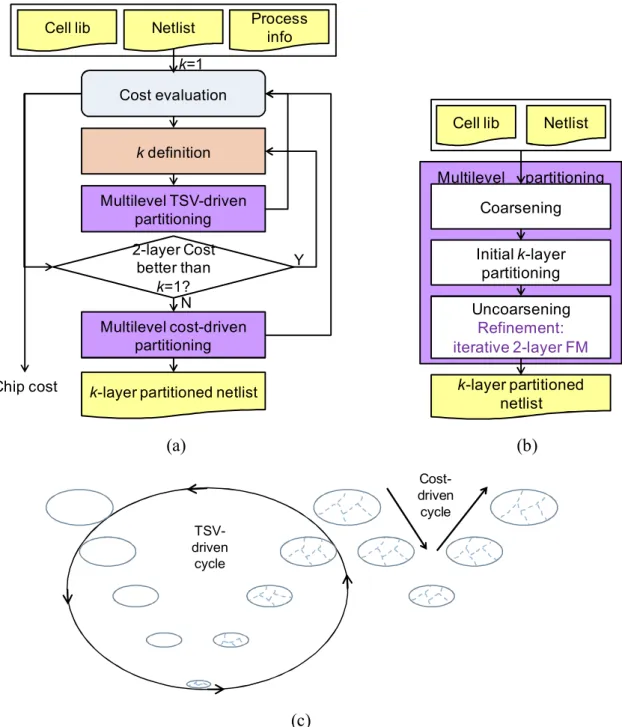
To conquer these issues, an efficient cost analyzer is desired. Dong and Xie proposed a system-level cost analyzer in [6]. On the contrary, to validate the cost estimation, we devise a circuit partitioning framework based on a given gate-level netlist. Unlike the existing TSV-aware methods, we also determine the number of layers
k to minimize the chip cost. If 2D IC is cheaper, k will be set to 1. First of all, we
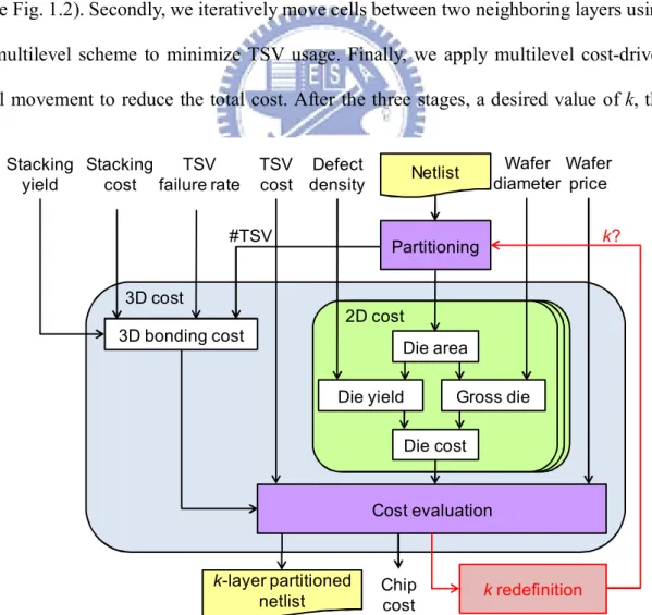
evaluate the total cost when k is 1 and determine the possible range of k with a low cost (see Fig. 1.2). Secondly, we iteratively move cells between two neighboring layers using a multilevel scheme to minimize TSV usage. Finally, we apply multilevel cost-driven cell movement to reduce the total cost. After the three stages, a desired value of k, the
Fig. 1.2. The cost evaluation of 2D and 3D ICs. Except the netlist, all parameters are given by the process information file.
Netlist
Die yield Gross die
Die cost k-layer partitioned netlist Cost evaluation Die area Wafer diameter Wafer price Chip cost TSV cost Defect density 3D bonding cost TSV failure rate Stacking cost Stacking yield Partitioning #TSV 2D cost 3D cost k? k redefinition
4
chip cost and TSV usage are obtained. Moreover, we reformulate Rent’s rule to facilitate the determination of k, and our results prove the correlation between Rent’s rule and TSV usage.
1.4. Organization
The rest of this thesis is organized as follows. Chapter 2 gives the problem formulation. In Chapter 3, we detail the proposed algorithms. Experimental results are present in Chapter 4. Finally, we briefly summarize the benefits of our algorithm in Chapter 5.
5
C
HAPTER
2
P
RELIMINARIES AND
P
ROBLEM
F
ORMULATION
In this Chapter, we will introduce terminology for 3D IC, partitioning techniques, and Rent’s rule, and finally give the problem formulation.
2.1. Stacking approaches of 3D ICs
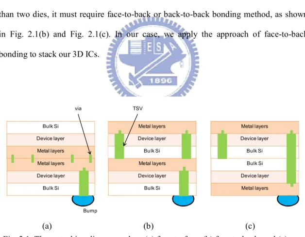
Fig. 2.1 shows that there are three approaches for stacking two dies. The face-to-face bonding, as shown in Fig. 2.1(a), is the best method due to it provides the short, tiny vias to connect dies. However, it is only suitable for two dies. To stack more than two dies, it must require face-to-back or back-to-back bonding method, as shown in Fig. 2.1(b) and Fig. 2.1(c). In our case, we apply the approach of face-to-back bonding to stack our 3D ICs.
(a) (b) (c)
Fig. 2.1. Three stacking die approaches: (a) face-to-face, (b) face-to-back, and (c) back-to-back. Metal layers Device layer Bulk Si Bulk Si Device layer Metal layers Metal layers Device layer Bulk Si Metal layers Device layer Bu lk Si Bulk Si Device layer Metal layers Metal layers Device layer Bulk Si Bump via TSV
6
2.2. TSV types
There are two types of TSVs to connect dies, as shown in Fig. 2.2. Since the diameter of TSV is positive correlated to the etched depth and technique, the diameter of via-last TSV is larger than that of via-first TSV. In this work, the TSV area is defined in the cell library. Table 2.1 shows the average cell area and TSV area in each benchmark. A typical size of via-first TSVs ranges from 1m to 10m, whereas that of via-last TSVs ranges from 10m to 50m [14]. Fig. 2.3 shows the TSV size versus the inverter size. To simulate the real case, we modify the cell library for bench6 and bench7, as shown in Table 2.1(b).
(a) (b)
Fig. 2.2. TSV types: (a) via-first TSV, (b) via-last TSV Table 2.1. (a) The average cell area vs. TSV area
(m2) bench1 bench2 bench3 bench4 bench5 bench6 bench7 bench8 Avg. cell area 49.55 50.02 41.12 42.03 51.89 47.18 42.68 46.28 Inverter area 19.5 ~30 19.5 ~30 16.5 ~25 16.5 ~25 16.5 ~25 16.5 ~25 16.5 ~25 16.5 ~25 TSV area 100 100 1600 1600 1600 900 900 1600
Table 2.1. (b) The average cell area vs. TSV area in modified cell library (m2) bench6 bench7
Avg. cell area 4.718 4.268 Inverter area 1.65 ~2.5 1.65 ~2.5 via-last TSV area 100 100 via-first TSV area 25 25 Metal layers Device layer Bulk Si Metal layers Device layer Bulk Si Metal layers Device layer Bulk Si Metal layers Device layer Bulk Si
7
2.3. The manufacturing cost
The manufacturing cost of 3D IC can be divided into three terms:
1.
Wafer manufacturing cost: It depends on the process of making products. Since the cost of a deep sub-micron process is very expensive, it occupies the most majority part of IC cost.2.
Testing cost: The testing cost is determined by the circuit complexity and testing time. Both of them can be compensated by an advanced testing methodology [16]. Hence, testing cost is not included in this thesis.3.
Assembly and packaging cost: Since the package of 2D chip is same as 3D chip, only the 3D bonding cost is considered.8
2.4. Cost formulae
Table 2.2 lists the related parameters indicated in Fig. 1.2 and Table 2.3 lists the values of five process information files; the reduced cost formulae [18] are as follows:
k i bonding i die total C C C 1 , ; (1) ; , die gdie TSV wafer i die Y N C P C (2) ; ) 1 ( ) 1 ( 1 TSV TSV k stacking stacking bonding F N Y C k C (3) ; 2 4 2 die wafer die wafer gdie A d A d N (4) ; 0 D A die die e Y (5) . ) 1 ( cell TSV die A A A (6)In (1), Ctotal is the total cost. It includes the cost of each die in 3D ICs and the bonding cost. In (2), the die cost is the cost of a good die in a wafer and the cost of a
Table 2.2. The parameters used in the cost model. Symbol Description Symbol Description
k The number of layers FTSV TSV failure rate
Ctotal Total cost Ydie Yield of dies
Cdie,i Die cost of layer i Ystacking Yield of die stacking Cbonding Bonding cost, 0 for 2D IC Adie Die area
Cstacking
Stacking cost for single
layer Acell Area occupied by cells and macros
CTSV TSV cost, 0 for 2D IC ATSV Area occupied by TSVs
Pwafer Single wafer price
Coefficient for routing area overhead
Ngdie The number of gross dies dwafer Wafer diameter NTSV The number of TSVs D0 Defect density
9
wafer includes the cost of processing TSVs for 3D ICs. In (3), the bonding cost correlates with k and the number of TSVs. The number of TSVs and k are larger, the bonding cost is more expensive. In (4), the number of good dies in a wafer is the total number of dies minus the number of cut dies in a wafer. In (5), the yield of a die correlates with the area of a die and the defect density of the process. In (6), the area of a die is the area of total cells in a die with considering routing overhead and the area of TSVs. Due to TSVs are directly connected with metal layers, we consider no congestion for TSVs while processing routing. Except k, NTSV, and Ctotal, the values of other parameters are defined in the process file. The cost model will be incorporated into our framework.
2.5.
Fiduccia-Matteyses min-cut Algorithm
The FM (Fiduccia-Matteyses) min-cut algorithm [13] provides an efficient approach to solve the problem of partitioning a circuit into 2 parts to minimize the number of cut nets. It calculates the gain of all cells and heuristically moves cells. We utilize FM to reduce TSVs with area constraint.
Table 2.3. The process information files. Symbol Value of Process_1 Value of Process_2 Value of Process_3 Value of Process_3m Value of Process_4 Cstacking 0.01 0.01 0.25 0.025 0.05 CTSV 150 150 250 250 150 Pwafer 4,000 8,000 8,000 8,000 8,000 FTSV 0.000001 0.000001 0.00001 0.00001 0.0001 Ystacking 0.99 0.99 0.985 0.985 0.98 0.3 0.3 0.33 0.33 0.33 dwafer 8 12 12 12 12 D0 5.0 4.0 1.0 0.5 1.0
10
2.6.
Coarsening technique
There are two kinds of hierarchical coarsening techniques, hyperedge coarsening (HEC) and edge coarsening (EC). Both are modified as modified hyperedge coarsening (MHEC) and FirstChoice (FC) [15]. We choose FC as our coarsening technique. FC coarsens cells based on the strength of connectivity by net weights. The weight of a net
ei is set as 1/(deg(ei) -1), where deg(ei) represents the degree of net ei. Each cell chooses
the strong connectivity cell to merge together.
2.7. Initial partitioning technique
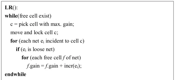
In the initial partitioning phase, we modify Loose net Removal (LR) algorithm [8] as our initial partitioning technique. LR focuses on the free cells of a loose net. Its goal is to prevent the loose net from being cut. According to the increased gain values, the highest priority cell moves to the locked region. The weight of loose net ei increase by
) deg( ) deg( ) deg( _ max_ ) ( i i e e i i F L e size net e
incr , where deg(ei) is the degree of net ei, deg(Lei) is
the number of locked cells in ei, deg(Fei) is the number of free cells in ei. The modified
LR algorithm is shown as Fig. 2.4.
Fig. 2.4. The modified loose-net removal algorithm
LR():
while(free cell exist)
c = pick cell with max. gain; move and lock cell c;
for (each net ei incident to cell c) if (ei is loose net)
for (each free cell f of net) f.gain = f.gain + incr(ei);
11
2.8. Problem Formulation
As shown in Fig.1.2, the problem formulation of this thesis is given the gate-level netlist of a design, the cell library, and the cost models for 2D and 3D ICs, find the minimum cost and the corresponding number of layers k, partition the design into k layers and insert TSVs accordingly.
12
C
HAPTER
3
C
OST
E
VALUATION AND
C
IRCUIT
P
ARTITIONING
Before proposing the algorithm, we show our observations. Secondly, our framework is proposed. As shown in Fig. 3.1(a), the major steps of framework are k definition, multilevel TSV- and cost-driven partitioning. The general view of multilevel partitioning is shown in Fig. 3.1(c). Since low TSV usage usually leads to low cost, we use TSV-driven partitioning to obtain a fast initial solution and then adopt cost-driven partitioning to further refine the cost.
3.1. Observations
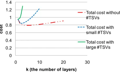
According to the cost formula (1), we try to simulate the impact of TSVs. Fig. 3.2 illustrates the curves of die cost, bonding cost and total cost if the impact of TSVs can be negligible and the die area keeps the same for all layers. For a real case—Bench_1, as shown in Fig. 3.3, with area balance for each layer, the curves are similar to the simulated ones except that the cost growth with TSV consideration is faster than that excluding TSV. Therefore, the simulated ones are reasonable and can simulate the impact of the number of TSVs for k.
As shown in Fig. 3.4, we can clearly see that the optimum k will be shrunk if the impact of TSVs is severe. According to Fig. 3.4, we can determine the maximum possible k without considering TSVs and without partitioning the design into k layers (k >2) if the cost of 2 layers is larger than the cost of 2D IC.
13
(a) (b)
(c)
Fig. 3.1. (a) The cost evaluation and partitioning framework of 2D and 3D ICs. Cost evaluation is detailed in Fig. 1.2. Automatic determination of k is based on the reformulated Rent’s rule. (b) The framework of multilevel TSV- or cost-driven partitioning. (c) Multilevel TSV- and cost-driven partitioning cycles.
Cost evaluation Netlist
k-layer partitioned netlist
Multilevel TSV-driven partitioning
Chip cost
Cell lib Process
info k definition Multilevel cost-driven partitioning k=1 2-layer Cost better than k=1? Y N Multilevel partitioning Netlist k-layer partitioned netlist Uncoarsening Refinement: iterative 2-layer FM Cell lib Initial k-layer partitioning Coarsening TSV-driven cycle Cost-driven cycle
14
Fig. 3.2. The curves of bonding cost, die cost and total cost.
Fig. 3.3. The curves of bonding cost, die cost and total cost by Bench_1.
Fig. 3.4. The impact of the number of TSVs 0 0.2 0.4 0.6 0.8 1 1.2 0 10 20 30 c os t
k (the number of layers)
Bonding cost w/o #TSV die cost w/o TSV area Total cost w/o TSV 0 0.2 0.4 0.6 0.8 1 1.2 0 10 20 30 c os t
k (the number of layers)
Total cost bonding cost die cost 0 0.2 0.4 0.6 0.8 1 1.2 1.4 0 10 20 30 c o s t
k (the number of layers)
Total cost without #TSVs
Total cost with small #TSVs Total cost with large #TSVs
15
Traditional Rent's rule [12] is based on recursive bi-partitioning. It is observed that the relationship between the numbers of external signal connections with the number of logic gates in the logic block, as shown in Fig. 3.5. The formula is T = tGα, where T is the terminals and G is the number of logic gates. t and α are solved by the statistic data of partitioning. In our experiments, we observe that the number of TSVs is directly proportional to the number of dies with similar number of cells in log-log graph, as shown in Fig. 3.6. Inspired by Rent’s rule, we replace the number of gates by the number of layers. Therefore, we utilize the equation of TSV-estimation, T = tkα, where T is the number of total TSVs, k is the number of layers, the parameter of t and α are solved by the data of k = 2 and kmax.
Fig. 3.7 shows that the TSV distribution is evenly distributed over all layers except the base layer because the base layer is designated for inputs and outputs. According to Fig. 3.6 and Fig. 3.7, we can also estimate the bonding cost and die cost. Therefore, the total cost can be estimated.
Fig. 3.5. # of terminals connected vs. # of gates (SLIP-2000) [17]. It is observed that the relationship between the numbers of external signal connections with the number of logic gates in the logic block. The formula of Rent’s rule is T = tGα, where T is the terminals and G is the number of logic gates. t and α are solved by the statistic data of partitioning.
16
3.2. Cost Evaluation and Partitioning Framework
3.2.1.
Multilevel TSV-driven partitioning
The flow chart of multilevel TSV-driven partitioning is shown in Fig. 3.1(b). TSV-driven partitioning is used to obtain an initial partitioned netlist with low TSV usage. First of all, we execute multilevel coarsening to reduce the problem size. Secondly, according to the connectivity, we assign the coarsened cells to the layer under the area constraint. Then the FM algorithm is executed between the two neighboring layers by the order shown as Fig. 3.8(a) to further minimize the number of TSVs.
Fig. 3.6. The number of layers vs. the number of TSVs in log-log graph.
Fig. 3.7. TSV usage in each layer versus k in Bench_1. 1 4 16 64 256 1024 4096 16384 65536 1 4 16 64 # o f T S V
k (the number of layers)
Bench_1 Bench_2 Bench_3 Bench_4 Bench_5 Bench_6 Bench_7 Bench_8 0 5 10 15 20 25 30 35 0 5 10 15 # o f T S V s p e r la y e r
k (the number of layers)
2nd layer 3rd layer 4th layer 5th layer 6th layer 7th layer 8th layer 9th layer 10th layer 11th layer
17
Finally, at the uncoarsening phase, and k-layer partitioning is executed iteratively until the declutered circuit is the original one. In the Chapter 4, we will take comparison for TSV usage by the different orders as shown in Fig. 3.8.
3.2.1.1. Multilevel coarsening
We utilize FC technique to coarsen the design iteratively until the number of new
(a) After processing the FM in upper layer, we then execute it downwards until the bottom (UB)
(b) After processing the FM upwards to the top layer, we then execute it downwards until the bottom (BTB)
(c) Execute FM from the top layer downwards to the bottom layer (T2B)
(d) Execute FM from the bottom layer upwards to the top layer (B2T)
Fig. 3.8. The right arrow is the step of the order of executing the FM in each approach. The double-headed arrow points the two layers executing the FM.
Layer 4 Layer 3 Layer 2 Layer 1 Layer 4 Layer 3 Layer 2 Layer 1 Layer 4 Layer 3 Layer 2 Layer 1 Layer 4 Layer 3 Layer 2 Layer 1 Layer 4 Layer 3 Layer 2 Layer 1 Layer 4 Layer 3 Layer 2 Layer 1 Layer 4 Layer 3 Layer 2 Layer 1 Layer 4 Layer 3 Layer 2 Layer 1 Layer 4 Layer 3 Layer 2 Layer 1 Layer 4 Layer 3 Layer 2 Layer 1 Layer 4 Layer 3 Layer 2 Layer 1 Layer 4 Layer 3 Layer 2 Layer 1 Layer 4 Layer 3 Layer 2 Layer 1 Layer 4 Layer 3 Layer 2 Layer 1 Layer 4 Layer 3 Layer 2 Layer 1 Layer 4 Layer 3 Layer 2 Layer 1 Layer 4 Layer 3 Layer 2 Layer 1
18
nets and cells are close to the previous one; the factors for nets and cells are set by 0.7
and 0.753/ k separately. FC coarsening technique is modified, where each group
consists of at most three vertices. In this phase, the area of groups is smaller than Amax = Acell/(50k), where Acell is the total area of the original design.
3.2.1.2. Initial partitioning
The inputs and outputs of a circuit are placed at the base layer. To assign the coarsened cells to the appropriate layer, we did it with FC, original LR, the strength of connectivity and modified LR. The results show the modified LR is the best one for initial partitioning. Therefore, we iteratively apply modified LR algorithm to choose the appropriate cell and then place the cell to the lowest layer which area is not larger than Athr = Acell/k until no free cells exist.
3.2.1.3. k-layer TSV-driven partitioning
If the cell is moved with a positive gain toward one side, it will be moved with a negative gain toward the opposite side. Therefore, we simplify the k-layer partitioning into two-layer partitioning with FM algorithm and balance area iteratively toward both sides.
3.2.1.4. Multilevel uncoarsening
There are two parts at this phase: local uncoarsening and global uncoarsening. For local uncoarsening, we decluster the coarsened cells connected with the cut nets; for global uncoarsening, we decluster all coarsened cells. Due to the FM cannot distinguish between the cells with same gain but different types, i.e. the gain of -3 plus 1 and the gain of -2 are same, we utilize local uncoarsening to reduce break-tie conditions.
19
Therefore, we execute both uncoarsening techniques iteratively with k-layer TSV-driven partitioning iteratively until the uncoarsed design is the original one.
3.2.2.
The Coarsening at The Same Layer and Multilevel Cost-
Driven Partitioning
Before processing the cost-driven partitioning, we apply FC algorithm to coarsen the cells at the same layer iteratively until the depth of coarsening is reached. During coarsening, each group consists of at most three vertices. Once the coarsening phase is done, the cost-driven k-layer partitioning is executed. In cost-driven partitioning phase, the uncoarsening technique is only global uncoarsening. At the cost-driven partitioning, the gain on cut size (TSV usage) is used to select the cell to be moved during FM, but cost is re-evaluated and recorded after each movement. At the end, the cost is used to determine the movements that should be applied.
3.3. k Definition
According to our observations, we develop two approaches to find the appropriate
k for the optimum cost of 3D ICs as follows.
3.2.1.
Rent’s Rule (RR)
First of all, if the cost of k = 2 is better than that of k = 1, k will be kmax in the second iteration. Based on the reformulated Rent’s rule, we interpolate the number of TSVs and the cost for an unsolved k. Moreover, our results show the strong correlation between the estimated and real TSV usages. (see Table 4.6)
20
As shown in Table 3.1, the numbers of TSVs in the middle layer of different k are close. Therefore, we can save time by assuming the number of TSVs In the middle layer of kmax as the results of k = 2. First of all, if kmax is even, we start with k = kmax, otherwise, we start with k = kmax +1. Secondly, the number of TSVs in middle layers is approximated by the results of k = 2. Finally, reformulated Rent’s rule is used to evaluate k. We take the evaluated k to execute the TSV- and cost-driven partitioning for 3D ICs.
Table 3.1. TSV usage in the middle layer of different k
#TSV k 2 4 6 8 10 12 14 16 18 20 Bench_1 25 27 27 27 27 27 25 25 25 25 Bench_2 261 261 261 261 261 261 261 261 261 261 Bench_3 1,597 1,612 1,617 1,879 1,648 2,177 1,637 1,654 1,728 1,628 Bench_4 1,146 1,143 1,143 1,143 1,148 1,150 1,151 1,143 1,151 1,151 Bench_5 1,066 1,068 1,066 1,070 1,177 1,066 1,236 1,253 1,241 1,236 Bench_6 339 2,029 1,430 1,430 1,430 1,430 1,433 1,430 1,434 1,431 Bench_7 1,079 1,079 1,088 1,079 1,169 1,087 1,557 1,437 1,089 1,675 Bench_8 1,265 1,297 1,297 1,297 1,297 1,297 1,305 1,298 1,298 1,359
21
C
HAPTER
4
E
XPERIMENTAL
R
ESULTS
4.1. Benchmark
Totally 10 industrial benchmarks [18] are used. Table 4.1 lists the benchmark statistics, where Circuit_1, Circuit_2, and Circuit_3 are used in [7]. Others are newly added. Table 2.3 lists the values of five process information files. Bench_1 uses Process_1, Bench_6 uses Process_3m, Bench_2, Bench_4 and Bench_7 use Process_2 and others use Process_3.
4.2. Experimental setting
Our framework is written by C/C++ language and executed on a platform with Intel Xeon CPU E5420 of 2.5 GHz frequency and of 32 GB memory.
4.3. Experimental methodology
To show that the approach of Rent’s rule is effective and efficient, we also proposed four approaches for comparison.
Table 4.1. Benchmark Information
Benchmark #Cells #Nets 2D cost (USD/chip) Circuit_1 6,290 6,512 Table 4.4(a) Circuit_3 9,155 8,627 Table 4.4(b) Bench_1 (a.k.a. Circuit_2) 85,013 89,187 0.920740 Bench_2 90,124 90,717 0.837453 Bench_3 399,048 401,426 3.195320 Bench_4 202,815 203,756 2.075460 Bench_5 482,189 484,738 5.457680 Bench_6 900,307 906,404 8.901710 Bench_7 468,536 472,278 8.635300 Bench_8 484,456 488,296 4.716000
22
4.3.1. Linear Increment/Decrement (LI)
Initially, k = 1. We start with k = 2, increase k by one if the cost of k is better than the previous one. Otherwise, we decrease k by one as the number of layers for 3D ICs.
4.3.2. Linear decrement (LD)
First of all, the costs of k = 1 and 2 are evaluated. If k = 2 with a smaller cost, it means that it is possible to get lower cost by partitioning the design into more dies. Secondly, the maximum possible k (kmax) is determined by the cost function with omitting the impact of TSVs. We start with kmax and decrease k by one if the cost of k is better than that of k+1 or larger than k =2. Finally, we can choose the best k as the number of layers for 3D IC.
4.3.3. Quadratic Equation (QE)
Since the cost function w.r.t. k is convex, we use a quadratic equation to fit this curve. At least three points are required. Initially, the three points are k = 1, 2, kmax. If the cost of k =2 is larger than that of k = 1, then k is set to as 1. Otherwise, we utilize the better k and its neighboring two points to get new k for lowering the cost. We iteratively confine the range of k until k is selected. Then we use LD and LI to check if k is fit.
4.3.4. Binary Search (BS)
Since the cost function is convex, binary search can be used in possible range of k to redefine k.
4.4. Discussion
Table 4.2 shows the comparison for TSV usage of the different orders of executing FM in Fig. 3.8. Due to the primary input and output are placed in the bottom layer, it is a good starting point for executing FM from the bottom to the top layer. Therefore, the method of B2T is better than the one of T2B. While processing the FM with B2T, the lower layer is different and the previous step cannot be guaranteed to be the best. The B2T is modified as the UB and the BTB. While processing the FM in the upper layer, only the UB can guarantee that the lower layers are the best. Therefore, the UB is the
23 best order for reducing TSV usage.
Comparison with [7] is listed in Table 4.3. It can be seen that we can generate competitive even better results than [7]. (The results of [7] are quoted from their paper. Since the platform is different, the runtimes are not shown here.) In Table 4.4, Circuit_1 and Circuit_3 are determined to be implemented by 1 layer, i.e., 2D IC, using five process information files. It can be seen that 3D IC is not always suitable for all designs, and we shall evaluate cost before adopting it.
Tables 4.5 list the cost comparison over all approaches of k definition. It shows that the steps of the definition of k and the cost corresponding to k during TSV-driven partitioning and the cost of the best k of 3D ICs by cost-driven partitioning in each
Table 4.2. TSV usage vs. the order of executing the FM in Fig. 3.8 while k is 10
Benchmark UB BTB T2B B2T Bench_1 245 245 245 240 Bench_2 2,273 2,273 2,273 2,273 Bench_3 12,490 12,489 12,568 12,681 Bench_4 11,122 11,887 16,077 13,117 Bench_5 9,334 9,522 10,878 9,456 Bench_6 11,385 11,385 11,395 11,587 Bench_7 9,726 9,726 10,633 9,731 Bench_8 9,703 9,703 10,305 9,759 Total 66,278 67,230 74,374 68,844
Table 4.3. Multilevel multilayer TSV-driven partitioning comparison.
Ours [7] Circuit_1 (4 layers) # of TSV Chip area 560 223,096.0 579 211,196.0 Circuit_2 (5 layers) # of TSV Chip area 119 1,465,465.0 157 1429,665.0 Circuit_3 (3 layers) # of TSV Chip area 378 269, 577.0. 285 273,211.5
24
approach. Determined k is k of the lowest cost between 2D and 3D ICs. All approaches can successfully find the appropriate value of k. It can be seen that runtime is directly proportional to the iterations of k definition. The numbers of iterations of the approaches of LI and LD depend on the design and the process. The approaches of QE and BS can have small numbers of iterations if the appropriate value of k is close to neither 2 nor kmax. The approaches of RR and FRR can find k within three iterations. Therefore, the runtimes are stable.
Table 4.6 shows the strong correlation of TSV usages estimated by Rent’s rule and the real number. It can be seem that the estimated TSV usage by Rent’s rule is close to the real one. Therefore, we can utilize Rent’s rule to estimate the TSV usage and bonding cost in different k. Since Bench_3 is suitable for 2D IC, it is not included here. Even when the estimated TSV number is biased, the trend could be accurate so that the bias would not affect the determination of k.
Table 4.7 shows that the TSV distribution is evenly distributed over all layers except the base layer in each benchmark. According to Table 4.6 and 4.7, we can also estimate the TSV usage and die cost in each layer. Once bonding cost and die cost are estimated, k of the best cost can also be determined.
Table 4.4. k for Circuit_1 and Circuit_3 (cost unit: USD/chip) (a) Circuit_1
k Process_1 Process_2 Process_3 Process_3m Process_4 1 0.030421 0.026914 0.027261 0.027227 0.027261 2 0.041854 0.037737 0.053843 0.053825 0.079807
Determined k 1 1 1 1 1
(b) Circuit_3
k Process_1 Process_2 Process_3 Process_3m Process_4 1 0.041814 0.036946 0.037375 0.037312 0.037375 2 0.053528 0.047870 0.064273 0.064239 0.090195
25
Table 4.8 shows our results of Rent’s rule compared with other participants’ results [20]. k is the number of dies of the lowest cost for 3D ICs in each participantsand the best k is the number of dies of the lowest cost for 3D ICs from each participants. We can see that we overcome them in most cases and our k is accurate.
Table 4.9 shows the results of simulated real cell library for Bench_6 and Bench_7. It shows that 3D cost is not lower than 2D cost in real cases of our designs and 3D ICs are suitable for larger designs.
26
Table 4.5. Cost comparison for different approaches of k definition (cost unit: USD/chip) (a) Bench_1 LI LD QE BS RR FRR k TSV-driven cost k TSV-driven cost k TSV-driven cost k TSV-driven cost k TSV-driven cost k TSV-driven cost 2 0.835175 2 0.835175 2 0.835175 2 0.835175 2 0.835175 6 0.799776 3 0.806017 6 0.799776 6 0.799776 4 0.796999 6 0.799776 5 0.796180 4 0.796999 5 0.796180 4 0.796999 5 0.796180 5 0.796180 5 0.796180 4 0.796999 3 0.806017 6 0.799776 6 0.799776 5 0.796180 Cost-driven cost 0.796088 0.796088 0.796088 0.796088 0.796088 0.796088 runtime (s) 74.12 58.03 74.19 58.15 46.45 30.40 2D cost 0.920740 Determined k 5 5 5 5 5 5 (b) Bench_2 LI LD QE BS RR FRR k TSV-driven cost k TSV-driven cost k TSV-driven cost k TSV-driven cost k TSV-driven cost k TSV-driven cost 2 0.766992 2 0.766992 2 0.766992 2 0.766992 2 0.766992 6 0.759070 3 0.748961 5 0.751824 5 0.751824 4 0.747337 5 0.751824 4 0.747337 4 0.747337 4 0.747337 3 0.748961 5 0.751824 4 0.747337 5 0.751824 3 0.748961 4 0.747337 3 0.748961 Cost-driven cost 0.747337 0.747337 0.747337 0.747337 0.747337 0.747337 runtime (s) 22.65 22.71 22.70 22.66 18.24 13.84 2D cost 0.837453 Determined k 4 4 4 4 4 4
27
Table 4.5. Cost comparison for different approaches of k definition (cost unit: USD/chip) cont. (c) Bench_3 LI LD QE BS RR FRR k TSV-driven cost k TSV-driven cost k TSV-driven cost k TSV-driven cost k TSV-driven cost k TSV-driven cost 2 3.319730 2 3.319730 2 3.319730 2 3.319730 2 3.319730 6 4.242050 2 3.319730 Cost-driven cost 3.318180 3.318180 3.318180 3.318180 3.318180 3.318180 runtime (s) 81.12 81.17 82.80 81.73 81.42 137.09 2D cost 3.195320 Determined k 1 1 1 1 1 1 (d) Bench_4 LI LD QE BS RR FRR k TSV-driven cost k TSV-driven cost k TSV-driven cost k TSV-driven cost k TSV-driven cost k TSV-driven cost 2 2.012910 2 2.012910 2 2.012910 2 2.012910 2 2.012910 10 3.874090 3 2.167450 9 3.880730 9 3.880730 4 2.349040 9 3.880730 2 2.012910 8 3.213080 3 2.167450 3 2.167450 3 2.167450 7 3.798270 6 2.760260 5 2.559090 4 2.349040 3 2.167450 Cost-driven cost 2.012700 2.012700 2.012700 2.012700 2.012700 2.012700 runtime (s) 66.51 250.14 97.15 93.77 98.04 71.94 2D cost 2.075460 Determined k 2 2 2 2 2 2
28
Table 4.5. Cost comparison for different approaches of k definition (cost unit: USD/chip) cont. (e) Bench_5 LI LD QE BS RR FRR k TSV-driven cost k TSV-driven cost k TSV-driven cost k TSV-driven cost k TSV-driven cost k TSV-driven cost 2 4.991380 2 4.991380 2 4.991380 2 4.991380 2 4.991380 8 5.746010 3 4.956400 8 5.746010 8 5.746010 4 5.057330 8 5.746010 3 4.956400 4 5.057330 7 5.845840 4 5.057330 3 4.956400 3 4.956400 6 5.283700 3 4.956400 5 5.105560 4 5.057330 3 4.956400 Cost-driven cost 4.956280 4.956280 4.956280 4.956280 4.956280 4.956280 runtime (s) 184.77 434.68 256.30 184.87 200.11 159.98 2D cost 5.457680 Determined k 3 3 3 3 3 3 (f) Bench_6 LI LD QE BS RR FRR K TSV-driven cost k TSV-driven cost k TSV-driven cost k TSV-driven cost k TSV-driven cost k TSV-driven cost 2 7.874910 2 7.874910 2 7.874910 2 7.874910 2 7.874910 10 8.332970 3 7.470410 10 8.332970 10 8.332970 4 7.681660 10 8.332970 4 7.681660 4 7.681660 9 8.302630 5 7.697060 7 7.765870 4 7.681660 8 8.291130 4 7.681660 3 7.470410 7 7.765870 3 7.470410 6 7.960550 Cost-driven cost 7.470410 7.765550 7.470410 7.470410 7.680890 7.680890 runtime (s) 395.99 908.37 641.21 522.36 459.89 337.59 2D cost 8.901710 Determined k 3 7 3 3 4 4
29
Table 4.5. Cost comparison for different approaches of k definition (cost unit: USD/chip) cont. (g) Bench_7 LI LD QE BS RR FRR k TSV-driven cost k TSV-driven cost k TSV-driven cost k TSV-driven cost k TSV-driven cost k TSV-driven cost 2 5.437360 2 5.437360 2 5.437360 2 5.437360 2 5.437360 18 5.712760 3 4.717470 17 5.509800 17 5.509800 4 4.471670 17 5.509800 6 4.386440 4 4.471670 16 5.365000 9 4.616470 10 4.685620 6 4.386440 5 4.445660 15 5.143090 8 4.519830 3 4.717470 6 4.386440 14 5.228030 7 4.461220 7 4.462200 7 4.461220 6 4.386440 5 4.445660 5 4.445660 6 4.386440 Cost-driven cost 4.386210 5.141280 4.386210 4.386210 4.386210 4.386210 runtime (s) 477.40 438.73 584.40 555.83 273.63 213.53 2D cost 8.635300 Determined k 6 15 6 6 6 6 (h) Bench_8 LI LD QE BS RR FRR k TSV-driven cost k TSV-driven cost k TSV-driven cost k TSV-driven cost k TSV-driven cost k TSV-driven cost 2 4.469450 2 4.469450 2 4.469450 2 4.469450 2 4.469450 8 5.320420 3 4.283170 8 5.320420 8 5.320420 4 4.646120 8 5.320420 3 4.283170 4 4.646120 7 5.275320 3 4.283170 3 4.283170 3 4.283170 6 4.888180 4 4.646120 5 4.874380 4 4.646120 3 4.283170 Cost-driven cost 4.282900 4.282900 4.282900 4.282900 4.282900 4.282900 runtime (s) 216.51 523.00 293.42 216.60 223.77 180.55 2D cost 4.716000 Determined k 3 3 3 3 3 3
30
Table 4.6. TSV usage: Rent’s rule vs. real value
Bench_1 Bench_2 Bench_4 Bench_5 Bench_6 Bench_7 Bench_8
kmin 2 2 2 2 2 2 2
kmax 6 5 9 8 10 17 8
k Rent’s Real Rent’s Real Rent’s Real Rent’s Real Rent’s Real Rent’s Real Rent’s Real 2 25 25 261 261 1,146 1,146 1,066 1,066 339 339 1,079 1,079 1,265 1,265 3 47 55 475 496 1,964 2,265 1,866 2,138 821 408 1,837 2,006 2,113 1,469 4 74 82 728 750 3,071 3,419 2,776 3,207 1,539 3,582 2,681 3,018 3,042 3,527 5 105 106 1,013 1,013 4,345 4,552 3,779 3,773 2,506 4,687 3,594 4,404 4,035 4,887 6 141 141 5,768 5,665 4,861 4,842 3,732 7,461 4,567 5,110 5,083 5,099 7 7,333 9,941 6,014 7,589 5,225 6,180 5,592 6,479 6,178 7,071 8 9,020 7,973 7,233 7,233 6,994 10,899 6,664 7,509 7,317 7,317 9 10,833 10,833 9,045 11,110 7,778 8,759 10 11,385 11,385 8,933 9,726 11 10,124 11,299 12 11,350 11,572 13 12,608 12,912 14 13,897 15,093 15 15,215 14,656 16 16,561 16,604 17 17,934 17,934
Table 4.7. TSV usage in each layer while k is 10 in each benchmark
layer Bench_1 Bench_2 Bench_3 Bench_4 Bench_5 Bench_6 Bench_7 Bench_8
2 30 241 1,587 1,922 343 1,269 982 164 3 26 257 1,678 1,133 585 1,327 976 1,424 4 32 266 1,663 1,180 1,144 1,261 950 1,432 5 27 248 1,666 1,144 1,308 329 1,299 1,378 6 27 261 1,648 1,148 1,177 1,430 1,169 1,297 7 26 245 1,587 1,179 1,375 1,449 1,118 1,297 8 26 239 1,763 1,145 1,119 198 1,105 846 9 27 263 439 1,134 1,215 2,078 1,074 930 10 24 253 459 1,137 1,068 2,044 1,053 935
31
Table 4.8. Cost comparison for other participants’ results (cost unit: USD/chip) (--: absence data information) [20]
ours 014 037 046 063 064 Benchmark 2D cost Best k k 3D cost k 3D cost k 3D cost k 3D cost k 3D cost k 3D cost Bench_3 3.1953 2 2 3.3182 2 3.1721 2 3.3235 2 3.3209 2 3.1763 2 3.3138 Bench_4 2.0755 2 2 2.0127 2 2.0279 2 2.0116 2 2.0130 2 2.0120 2 2.0234 Bench_5 5.4577 3 3 4.9563 3 4.7939 3 4.9570 3 4.9612 2 5.0855 3 4.9819 Bench_6 8.9017 4 4 7.6809 4 7.6833 -- -- 4 7.4365 -- -- 3 7.4752 Bench_7 8.6353 6 6 4.3862 3 4.7174 5 4.6417 5 4.4242 2 5.4569 4 4.5754
Table 4.9. Simulated real case by Rent’s rule approach (cost unit: USD/chip)
via-first via-last
Bench_6 Bench_7 Bench_6 Bench_7
k TSV-driven cost k TSV-driven cost k TSV-driven cost k TSV-driven cost 2 0.688674 2 0.325869 2 0.691711 2 0.336091 Cost-driven cost 0.688674 0.325869 0.691711 0.336087 2D cost 0.655562 0.324582 0.655562 0.325482 Determined k 1 1 1 1
32
Chapter 5
Conclusions
According to [7], they utilize the multi-way partitioning to handle the multi-layer partitioning, while we proposed the two-way partitioning to do that. Furthermore, we propose a cost evaluation and partitioning framework for 3D IC. It can automatically determine the number of layers with the minimum cost. Moreover, we verified the effectiveness of determining the number of layers by six approaches. Especially, TSV usage can be estimated by the reformulated Rent’s rule. We also propose a fast approach. Our approach can handle large k and make good estimation of k in not gate-level but system-level circuits. Our k is the same as k determined by the best cost.
33
Bibliography
[1] International Technology Roadmap for Semiconductors (ITRS), http://www.itrs.net/. [2] W. R. Davis, J. Wilson, S. Mick, J. Xu, H. Hua, C. Mineo, A. M. Sule, M. Steer, and P. D. Franson, “Demystifying 3D ICs: the pros and cons of going vertical,” IEEE
Design & Test Magazine, vol. 22, no. 6, pp. 498--510, Nov.-Dec., 2005.
[3] W.-L. Hung, G. Link, Yuan Xie, N. Vijaykrishnan, and M. J. Irwin, “Interconnect and thermal-aware floorplaning for 3D microprocessors,” in Proc ISQED, pp. 98--104, Mar. 2006.
[4] R. Weerasekera, L.-R. Zheng, D. Pamunuwa, and H. Tenhunen, “Extending systems-on-chip to the third dimension: performance, cost and technological tradeoffs,” in Proc ICCAD, pp. 212--219, Nov. 2007.
[5] C. Ababei, Y. Feng, B. Goplen, H. Mogal, T. Zhang, K. Bazargan, and S. S. Sapatnekar, “Placement and routing in 3D integrated circuits,” IEEE Design & Test
Magazine, vol. 22, no. 6, pp. 520--531, 2005.
[6] X. Dong and Y. Xie, “System-level cost analysis and design exploration for three-dimensional integrated circuits,” in Proc ASP-DAC, pp. 234--241, Jan. 2009. [7] Y. C. Hu, Y. L. Chung, and M. Chen Chi, “A multilevel multilayer partitioning
algorithm for three dimensional integrated circuits,” in Proc ISQED, pp. 483--487, Mar. 2010.
[8] J. Cong, P. Li, S. K. Lim, T. Shibuya, and D. Xu. “Large scale circuit partitioning with loose/stable net removal and signal flow based hierarchical clustering,”
Technical Report 970005, CS Dept. of UCLA, 1997.
[9] D. H. Kin, K. A. and S. K. Lim, “A study of through-silicon-via impact on the 3D stacked IC layout,” in Proc ICCAD, Nov. 2009.
34
[10] I. H. R. Jiang, “Generic integer linear programming formulation for 3D IC partitioning,” in Proc SOCC, Sep. 2009.
[11] J. Cong and G. Luo, “A multilevel analytical placement for 3D ICs,” IEEE Circuits
and Systems Society, pp. 361-366, 2009.
[12] B. S. Landman and R. L. Russo. “On a pin versus block relationship for partitions of logic graphs,” IEEE Trans Comput., vol. C-20: pp. 1469--1479, 1971.
[13] C. M. Fiduccia and R. M. Mattheyses, “A linear time heuristic for improving network partitions,” In Proc DAC, pp. 175--181, 1982.
[14] S.K. Lim, “TSV-Aware 3D Physical Design Tool Needs for Faster Mainstream Acceptance of 3D ICs,” Design Automation Conference Knowledge Center Article, 2010.
[15] G. Karypis and V. Kumar. “Multilevel k-way hypergraph partitioning,” Technical
Report TR 98-036, Department of Computer Science, University of Minnesota,
1998.
[16] X. Wu, Y. Chen, K. Chakrabarty, and Y. Xie, “Test-access mechanism optimization for core-based three-dimensional SOCs,” in Proc ICCD, pp.212--218 Oct. 2008.
[17] P. Christie and D. Stroobandt, “The Interpretation and Application of Rent's Rule,”
IEEE Trans. on VLSI Systems, Special Issue on SLIP, vol. 8, no. 6, pp. 639-648,
2000.
[18] Provided by Industrial Technology Research Institute (ITRI), Hsinchu, Taiwan, 2009 and 2010.
[19] S. K. Lim, “TSV-based 3D IC Research Activities," at the Georgia Tech
Computer-Aided Design (GTCAD) Laboratory,
35
[20] Computer-Aided-Design (CAD) contest,
![Fig. 1.1. A 3-layer 3D IC with TSVs for connecting each die [10].](https://thumb-ap.123doks.com/thumbv2/9libinfo/8464532.183304/11.892.217.697.735.1090/fig-layer-d-ic-tsvs-connecting-die.webp)

![Fig. 2.3. TSV size versus inverter size (unit: m) [19]](https://thumb-ap.123doks.com/thumbv2/9libinfo/8464532.183304/16.892.164.777.124.671/fig-tsv-size-versus-inverter-size-unit.webp)
![Table 2.2 lists the related parameters indicated in Fig. 1.2 and Table 2.3 lists the values of five process information files; the reduced cost formulae [18] are as follows:](https://thumb-ap.123doks.com/thumbv2/9libinfo/8464532.183304/17.892.143.789.151.490/related-parameters-indicated-process-information-reduced-formulae-follows.webp)